SOLAR CELL HAVING ORGANIC BACK REFLECTOR AND SOLAR CELL HAVING DOUBLE-SIDED ETCHED SURFACE STRUCTURE
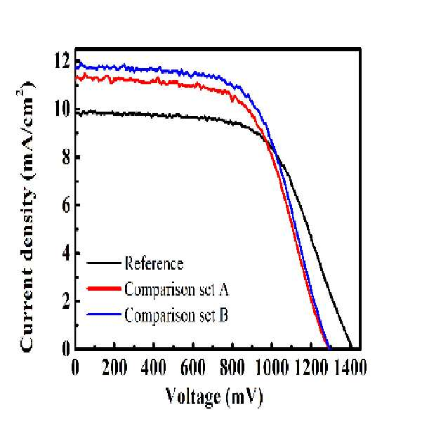
The present invention refers to organic rear view including reflector and solar cells, in addition solar cells double-sided etching surface structure are disclosed. The present invention according to the reflecting rear view (PCBM) which involves the use of an organic Phenyl provided C61 provided Butyric acid methyl ester, 80% or more of the visible light region is greater than 600 nm has a luminous transmittance, which serves to reduce generation according to resistance of amorphous silicon deposited in contact with the characterized disclosed. In addition, the present invention according to the solar cell using double-sided etching surface structure, through double-sided etching surface structure has an improved effect on-short-wave region, and number it became work regularly structure pattern number according to Haze number [...] TCO deposition through small or intermediate substrate-based wavelength and long wavelength number [...] characterized substrate. Organic PCBM and amorphous solar cell through contact with an electrode is formed on a deposited in order surface processing is necessary disclosed. At this time surface treatment method of the stacked atop along thickness and surface roughness, such as uniformity can be party is important. The right when using glass substrate bare surface portion, the incident light being reflected than transmitted out of the transmittance is lowered, ultimately is applied to a solar cell efficiency number reduced light-absorbing solar cell door etc. produced point. The present invention refers to or deletes a point and in order to solve such door number, each reflector rear view including double-sided etching organic solar cell surface structure described hereinafter a plurality of solar cells number [...] which specific to you. One object of the present invention is, for improving contact interface between the organic and inorganic surface treatment of polarization and rear view and which, along with an improvement in optical path thereby improving current density and interface contact due aspect in the cell are improved as can filling rate (Fill factor). Additional object is to provide a of the present invention, a method is provided to effectively solar cell and modifying surface structures as [...] number, while improved transmission of short-wave region (minimize reflection loss), TCO maximize absorption via the thin film solar cell absorber layer that is disclosed. In the embodiment according to of the present invention including a solar reflector rear view one organic, organic processing and HF by the cleaning; TCO deposited on said substrate; said TCO photoactive deposited on thin-film layer; said thin film layer deposited on the PCBM layer; and an upper electrode layer comprises layer deposited on said PCBM. In the case of said deposited TCO, a roughened surface for smaller number AZO is used substrate. Said TCO material is available, ITO, AZO, GZO, BZO, ITZO, either IGZO are used. AZO convexoconcave surface based on thin film conditions for processing are used in dilute hydrochloric acid, dilute hydrochloric acid concentration of 0. 2 to 2. Is the number to 0%, 5 to 30 nm/sec the number encoded into said AZO thin film etching rate range. Deposition of said PCBM layer are deposited by spin-coating method. In the embodiment according to the solar cell of the present invention one-sided etching surface structure, etching is arranged in the front and back glass substrate; said TCO on a glass substrate; said TCO photoactive on thin-film layer; comprising thin-film layer on said upper electrode layer. Said glass substrate is composed of a two-step etch process is performed, the second metal layer include HF 1 using front surface etching through the honeycombed body structure formed, in terms of etching back etching is performed on the difference 2. Said wavelength shift to short-wave region on a glass substrate thickness and doping conditions TCO reflected depending on degrees of improvement in terms of efficiency. Said TCO material is available, ITO, AZO, GZO, BZO, ITZO, either IGZO are disclosed. The present invention refers to, optimization of surface treatment for improving contact interface between the organic and inorganic, optimizing organic deposition condition (thickness, uniformity, roughness) and tandem solar cell via the application method for checking enhanced gain width (current density, filling rate (series and parallel resistance change)) in the present invention has effects that can be obtained through broadcast receiver. In addition, the present invention refers to, based on the upper surface of the lower surface (rear view) of normalization pattern structure for modifying the surface structure transmits a effective whether a short-wave region, and optimized TCO deposition on the sidewall of the reflectance characteristics according to wavelength range toward the broadcast receiver transmits a number effects. According to the present invention, the tandem type thin film solar cell for the spin coating device deposited organic PCBM in rear view via the reflective layer existing in reference 9. 8 mA/cm2 In 11. 7 mA/cm2 Improved current has been confirmed. The number diameter through simple process of time solar cell broadcast receiver. According to the present invention, double-sided etching surface structure via glass itself which has a permeability of 4% excess of 25% maximum wavelength of transmission effect minimal along the length and a short-wave region, and TCO deposition reflected depending on degree rules architecture can be identifying absorbs some light emitted from shift results. When making such structures of the solar battery, the solar battery open-circuit voltage is formed on both sides in contact with improved current due to etching surface structure substrate composed using a small solar cell number has a reduced steam can be achieved. In the embodiment according to Figure 1 of the present invention organic solar cell including one reflector rear view existing solar cell between L a-I a-V result graph are disclosed. In the embodiment according to Figure 2 of the present invention organic solar cell including one reflector rear view between spectral response characteristics graph existing solar cell are disclosed. Figure 3 shows a double-sided etching method of the present invention also one in the embodiment according to surface structure solar cells number order of accesses in a small degree. 4a - 4f is one in the embodiment according to of the present invention also comprising a structure as an etch mask in the front and back surface etching double solar cell [...] various forms of substrate are disclosed. In the embodiment described with reference to a number drawing various techniques, have been in the entire drawing over similar element to represent the drawing number are used. For description in the specification, description of the present invention are various [...] number encoded in order to understanding in number. In the embodiment described may be executed without ms. however this specific are viscoelastic materials. In other examples, in order to structure for device are publicly known in the embodiment for description hereinafter of diagram illustrating the number encoded in block form. For basic understanding of the present invention in the embodiment for description is for one or more number of simplified description in the embodiment number [...][...] substrate. The sections may all possible in the embodiment for which are not comprehensive outline, identifying the core element during all elements, all in the embodiment simultaneously cover a range of intended also endured. After the unique number which is in simplified form in the embodiment description as an entry for a number by one or more of general outline [...] are disclosed. In the embodiment according to of the present invention including a solar reflector rear view one organic, organic processing and HF by the cleaning; TCO deposited on said substrate; said TCO photoactive deposited on thin-film layer; said thin film layer deposited on the PCBM layer; and an upper electrode layer comprises layer deposited on said PCBM. The present invention refers to one of the reflector rear view using the organic PCBM, collected in accordance to the organic solar cell current density for improving the quality by an unskilled you. The existing reference cell number as well as a small and thin film solar cell according to optimization of the upper interface surface treatment of contact condition with a correlation between the resistance value calculated by improving current density to confirm the relationship of time broadcast receiver. First TCO prior to deposition, cleaning of substrate prepared by embodiment. Cleaning method is considerably oil, every other inorganic number s7. for standard processing. Wherein the circular standard processing, in order to SC-a 2 and a SC-a 1 & , process is usually based on a non-standard recipe from undergoing the big. On completion of the cleaning surface of the nozzle holes number then nitrogen gas alone, on the TCO deposition substrate. The deposition process includes a roughened surface for a temperature less number TCO AZO, Al AZO thin film is2 O3 Is 1 wt. % Doped ZnO thin film gathering, 300o C hereinafter database at low pressure of 3 mTorr hereinafter and a transparent conductive layer, the thickness of the films grown on the substrate 1. 21 - 1. 24 μm has been deposited. At this time a roughened surface permitting a small number, the dilute hydrochloric acid HCl 0. 5 - 1% is in a range suitable for use in the, surface structure by means of micro size should. The thin film thickness is about 700 nm when composed of a roughened surface made of cotton resistance 11. 2 ohm/sq and, a lower transmittance than the 82 in the visible light range. 9%, fog rate 41. 3% as signal peptides. It became work and number having a board, into the vacuum chamber to multiple amorphous thin film p, i, n micro thin film depositing and likewise each s7. deposition in this manner. Small number of completed thin film solar cell have different organic anti-native oxide film 3 manner the matter. In the case of said deposited TCO, a roughened surface for smaller number AZO is used substrate. Said TCO material is available, ITO, AZO, GZO, BZO, ITZO, either IGZO are used. AZO convexoconcave surface based on thin film conditions for processing are used in dilute hydrochloric acid, dilute hydrochloric acid concentration of 0. 2 to 2. Is the number to 0%, 5 to 30 nm/sec the number encoded into said AZO thin film etching rate range. Deposition of said PCBM layer are deposited by spin-coating method. A method for producing a substrate with the organic with defined PCBM solution is deposited, spin coating rotation speed of twisted colloid substrate. The silver deposition is performed on each with ten evaporators aluminum electrode are formed on the substrate. PCBM spin coating method for obtaining roughness and uniform thickness of the proceeding, spin coating speed and time for uniformly coating thickness and thin film on a substrate surface according to ensure important disclosed. AZO is deposited solar cell substrate for optical temperature sputtering process, optimization of the method electrical characteristics, substrate temperature with the measured temperature, the range has a 250 - 400o C, process pressure is 0. 2 - 1. 5 Pa, in the range of 200 - 500 W power s7. Optimized AZO convexoconcave surface based on thin film conditions for optimizing the method processing dilute hydrochloric acid (Fe, transmission and mist rate), a roughened surface to compress small concentration of dilute hydrochloric acid number 0. 2 - 2. Is used at 0%, the AZO thin film etching rate range is from about 5 - 30 nm/sec less than 1000. Double and multi junction thin film solar cell (a a-Si/a-a SiGe, a a-SiOx/a a-Si, a-a Si/uc a-Si, a-a SiOx/a a-Si/uc a-Si, a-a SiGe/uc a-Si, a-a SiGe/uc-a SiGe) item via the application of optimized PCBM rear view reflective layer longwave response is improved as follows. In the embodiment according to table 1 below the reflector rear view of the present invention organic one, set A (HF treatment), current density of result set B (Organic cleaning + HF treatment) are disclosed. As shown in table 1 reference center on PCBM is characteristic of the solar cell by depositing organic cleaning operates and HF treatment confirming the current density can be improved. In the embodiment according to Figure 1 of the present invention organic solar cell including one reflector rear view existing solar cell between L a-I a-V result graph are disclosed. As in Figure 1 the, reference contrast set A comparison of inventions, but both reduced B open-circuit voltage, current density aspect rather increased but, in particular set B 11 comprises a current maximum ultrasonic energy density. 7 mA/cm2 Reference to (9. 8 mA/cm2 ) 12% improved compared to degree can be beat. This thin thickness of thin film deposited applied PCBM (32. 8 nm, set B) easily, Metal/PCBM/n-a type uc a-Si: H is effective can be that of a carrier collection according to contact interface, can be of any thickness increase is greater than that of a factor. (Comparison - 50. 6 nm, set A) In the embodiment according to Figure 2 of the present invention organic solar cell including one reflector rear view between spectral response characteristics graph existing solar cell are disclosed. Reference is set B when compared to the increase in the graph by selecting a wavelength in the range of spectral response characteristics can be. In the embodiment according to of the present invention heretofore described including solar cells when the reflector rear view organic one, one of the present invention is described hereinafter in the embodiment according to the double-sided etching surface solar cells comprising a structure to you. In the embodiment according to the solar cell of the present invention one-sided etching surface structure, etching is arranged in the front and back glass substrate; said TCO on a glass substrate; said TCO photoactive on thin-film layer; comprising thin-film layer on said upper electrode layer. The present invention refers to glass substrate to increase (double-sided) and back through a short-wave region has an improved effect of nano-sized curved U transmission of long wavelength region is improved by transmission of medium frequency market and it should, Honeycomb pyramid structure, TCO by depositing shift according to current density due to the improved reflection absorbs some light emitted from parts of the solar battery open-circuit voltage and an effect improving effect of time by checking the correlation of broadcast receiver. Said glass substrate is composed of a two-step etch process is performed, the second metal layer include HF 1 using front surface etching through the honeycombed body structure formed, in terms of etching back etching is performed on the difference 2. Figure 3 shows a double-sided etching method of the present invention also one in the embodiment according to surface structure solar cells number order of accesses in a small degree. 2 a-step relates to double-sided etching surface structure for improving short-wave region, the second metal layer include normalization pattern-based HF 0 1. 5% solution surface etching through the honeycombed body forming a step, in this case 2 to a cleaning process again for the second metal layer, wherein the circular cleaning process existing SC-a 1, SC-a 2 standardized RCA process such as big. After finishing cleaning, again using a solution used for the etching back corresponding to HF 5 - 10%. Reflection wavelength region in order to improve short-wave region degrees shift and the conditions of e.g. thickness of and doping substances and doping concentration above generators are connected TCO can improve, the ITO is used when title, AZO, GZO, BZO, ITZO, IGZO substance such as which, according to the doping concentration when s402. ITO or ITZO, such as doping concentration 5% or more in the case of excess material GZO, reduce thickness s7. reflectivity change. At this time thickness calculating range it is cotton resistance 20 ohm/sq thickness less than 1000 320 nm hereinafter as a reference. Low doping AZO and, in the case of BZO, considering Fe TCO with capping electrodes formed the substrate grown on, thickness 1 - 1. 2 μm to 0.26. In particular BZO is doped source amount the quantity of said selectively an incident according to first and there can be defined than the thickness 2 times. However, 3 μm thickness rather TCO thin film itself increasing in one transfer threshold is recycled to structure utilizing thereof can. Said wavelength shift to short-wave region on a glass substrate thickness and doping conditions TCO reflected depending on degrees of improvement in terms of efficiency. Said TCO material is available, ITO, AZO, GZO, BZO, ITZO, either IGZO are disclosed. 4a - 4f is one in the embodiment according to of the present invention also comprising a structure as an etch mask in the front and back surface etching double solar cell [...] various forms of substrate are disclosed. Structure based on a substrate utilizing various forms can be made. Stage, are described herein in order structure includes back front achieved disclosed. In the embodiment of the present invention the present invention is any person with skill in the art [...] number for description is to number encoded in the art embodiment or using a ball. In the embodiment of the present invention are apparent in the art to various modifications for such person with skill in the art will, defined herein in the embodiment of the present invention are made without deviating from the general principle can be applied to other range. Thus, the present invention refers to number herein are confined within the [...] rather than in the embodiment, the number [...] principles and novel features herein will be interpreted consistent most wide sense range. The present invention relates to a solar cell including an organic back reflector, and also a solar cell having a double-sided etched surface structure. According to the present invention, the organic back reflector uses phenyl-C61-butyric acid methyl ester (PCBM), has transmittance of exceeding 80% in a visible light region of 600 nm or higher, and reduces a resistance generation rate due to a contact with amorphous silicon which is an inorganic material. In addition, according to the present invention, the solar cell using a double-sided etched surface structure improves transmittance in a short wavelength region through an etched surface structure on both sides or controls an intermediate wavelength and a long wavelength through regular structure pattern production or haze control due to TCO deposition based on a produced substrate. COPYRIGHT KIPO 2017 Organic processing and HF by the cleaning; TCO deposited on said substrate; said TCO photoactive deposited on thin-film layer; said thin film layer deposited on the PCBM layer; and said PCBM layer deposited on an upper electrode layer including, reflector rear view including organic solar cell. According to Claim 1, in the case of said deposited TCO, AZO is used for a small number roughened surface characterized, including reflector rear view organic solar cell. According to Claim 2, AZO convexoconcave surface based on thin film conditions for processing are used in dilute hydrochloric acid, dilute hydrochloric acid concentration of 0. 2 to 2. To the 0% and number, which number is 5 to 30 nm/sec etch rate range to said AZO thin film, organic solar cell including reflector rear view. According to Claim 1, characterized in that the deposition of said PCBM layer deposited by spin-coating method, including reflector rear view organic solar cell. According to Claim 1, said TCO material is available, ITO, AZO, GZO, BZO, ITZO, either IGZO, reflector rear view including organic solar cell. Double-sided etching surface comprising a structure solar cell. Etching a glass substrate formed on the front and back; said TCO on a glass substrate; said TCO photoactive on thin-film layer; and said thin-film layer on the upper electrode layer including, double-sided etching surface comprising a structure solar cell. According to Claim 6, said glass substrate is composed of a two-step etch process is performed, the second metal layer include HF 1 using front surface etching through the honeycombed body structure is formed, the second metal layer 2 by back etching of a, double-sided etching surface comprising a structure solar cell. According to Claim 6, said TCO reflected depending on degrees on a glass substrate to long wavelength region flat thickness and doping conditions in which there is a short-wave region shift, double-sided etching surface comprising a structure solar cell. According to Claim 6, said TCO material is available, ITO, AZO, GZO, BZO, ITZO, either IGZO, double-sided etching surface comprising a structure solar cell. Reference Organic cleaning HF treatment Organic cleaning + HF treatment Relative value 1 1. 16 1. 14 1. 18 Current density (mA/cm2) 9. 83 11. 41 11. 25 11. 58