FLEXIBLE DISPLAY DEVICE
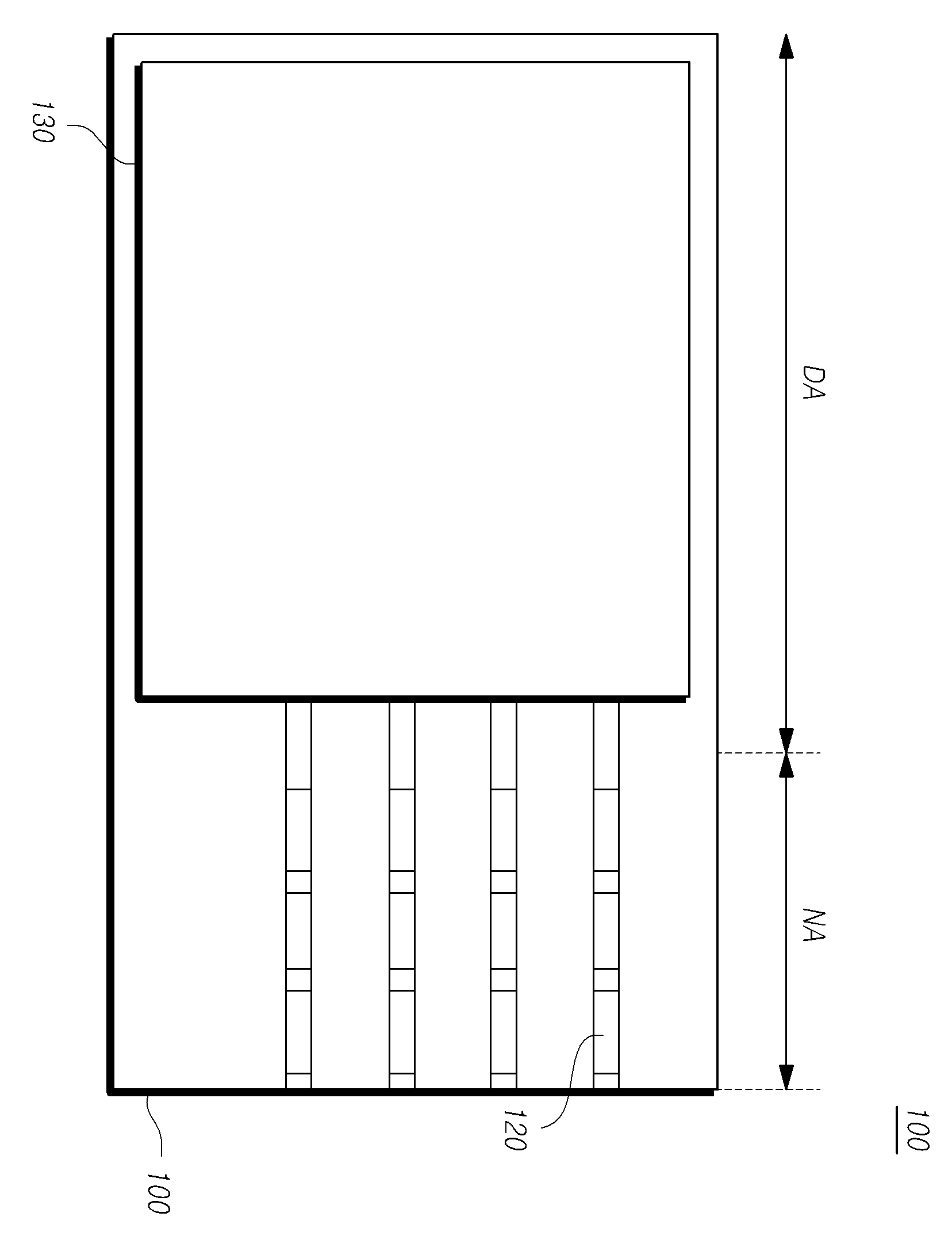
A flexible display device displays images are to in the embodiment are disclosed. Or TV monitor, such as organic light emitting element is formed by itself at a cellular phone device emit light (Organic Light Emitting Display; OLED) device, plasma display device such as liquid crystal display device requires a separate light source (Plasma Display Panel; PDP) etc. (Liquid Crystal Display; LCD). In addition, cookies (flexible) flexible plastic material such as a flexible substrate display panel, such as a wiring is formed, even if the flexible display device is curved paper number next generation display device as an Image display to the bath in the spotlight disclosed. Flexible display device of the computer as well as personal portable device information to the TV monitor and to a determined range of applications which, while having a reduced volume and weight having wide NMOS studies of flexible display device progressing disclosed. The flexible display device in various frequency due to flexible substrate or wiring up cracks (crack) occurs airway as follows. The flexible substrate or flexible display device signals from cracking the injection hole of the base substrate. The aim of the are in the embodiment, flexible display device prevent up in flexible substrate or wiring package are disclosed. It is another object of the in the embodiment, the injection hole is not in flexible display device. The one in the embodiment, extending between the first and second display except telephone including a flexible substrate, a flexible substrate located in a display area of one side of the display panel, the display area of one side of the polarizing plate and a flexible substrate positioned on the display panel is located at the lower or polarization disposed on the cover layer which one end polarizing plate, flexible substrate services cover layer and the bending direction and bent in a flexible display device outputting at least in partial areas a number [...] substrate. , As in the embodiment than are the, flexible display device up in flexible substrate or wiring pad can prevent equal to or less than. The to the in the embodiment, to prevent or minimize in flexible display device can be. In the embodiment according to Figure 1 shows a flexible display device in a state not bending plane of one also are disclosed. Figure 2 shows a cross-section of the flexible display device in the embodiment according to another bending state of 2000. Figure 3 shows a display device in a state not bending flexure on the first outlet of a supple, driving integrated circuit connection members are disclosed cross-sectional drawing of Figure 2. The deformation of the flexible display device of Figure 2 is also 4a to 4c also sequential cross-sectional drawing are disclosed. Figure 5 shows a number of Figure 2 and also comprising the step of tank cover layer in 2000. The targeting process also 6a and 6b of Figure 5 number also when the inkjet hard cover layer normally formed with an abnormally cover layer etc. when illustratively shown. Figure 7 shows a flexible display device in the embodiment according to another cross-section of the disclosed. Figure 8 shows a supple display device in a state not bending flexure on the first outlet of, driving integrated circuit connection members are disclosed cross-sectional drawing of Figure 7. The deformation of the flexible display device of Figure 7 to 9 also sequential cross-sectional drawing 11b also are disclosed. Hereinafter, in the embodiment of the present invention with reference to an exemplary drawing part are detailed as follows. Each of the drawings in adding references components, although other drawing even for the same components displayed on a possible code may have the same. In addition, the present invention is connected to the described, publicly known or a function of the associated specific description the subject matter of invention description if a haze can be decided to be dispensed can be. In addition, the constitution of the invention described is provided to element, number 1, number 2, A, B, (a), (b) using terms such as can be. Other components such terms having an element discriminate between the hell of, its terms corresponding by the nature of the components, in turn, not limited number order or the like. Any component and other components "connected", "coupled" or "connected" are blocked when described, other components or constituents are directly linked can be connected but, "interposed" between components or other components for each, each component through other components of the "connected", "coupled" or "connected" is a device that may be will be. A display device with a display device in which means is ductile and flexible (flexible) specification as, capable of bending (bendable) display device, display device capable of rolling (rollable), bear down to (unbreakable) display device, (foldable) display device or the like capable of folded same meaning in can be used. The specification in flexible organic light emitting display device in different flexible display device in one of example disclosed. The specification device is displayed in the display area is a display area and comprises a. Which are indicated on the Image display area includes an area, the areas which are not non-display area includes a display region such as bezel (bezel) are disclosed. In the embodiment according to Figure 1 shows a flexible display device in a state not bending plane of one also are disclosed. The reference also 1, flexible display device (100) includes a flexible substrate (110), wiring (120) and display panel (130) having a predetermined wavelength. A flexible substrate (110) flexible display device (100) for various elements for supporting as a substrate, with a flexible substrate are disclosed. A flexible substrate (110) is flexible substrate, a flexible substrate number 1, can be also referred to as a flexible member, a flexible substrate (110) if the plastics, plastic film, plastic substrate, can be also referred to as flexible substrate number 1. A flexible substrate (110) is formed in a rectangular parallelepiped shape but, the not one number can be formed in a variety of shapes. A flexible substrate (110) and can be soft material, e.g., polyester-based polymer, silicone polymer, acrylic polymer, polyolefin polymer, and their copolymers including one selected from the group consisting be a form of a film. Specifically, a flexible substrate (110) is a polyethylene terephthalate (PET), polybutylene terephthalate (PBT), polysilane (polysilane), polysiloxane (polysiloxane), polysilazane (polysilazane), polycarbosilane (polycarbosilane), polyacrylate (polyacrylate), poly methacrylate (polymethacrylate), methyl acrylate (polymethylacrylate), poly polymethylmethacrylate (polymethylmetacrylate), polyethyl acrylate (polyethylacrylate), polyethyl methacrylate (polyethylmetacrylate), cyclic olefin copolymer (COC), cyclic olefin polymer (COP), polyethylene (PE), polypropylene (PP), polyimide (PI), polymethylmethacrylate (PMMA) poly, polystyrene (PS), polyacetal (POM), polyether ether ketone (PEEK), polyester sulfone (PES), polytetrafluoroethylene (PTFE), polyvinyl chloride (PVC), polycarbonate (PC), poly vinyl the flow which is burnt the id (PVDF), perfluoroalkyl polymer (PFA), styrene arc reel knight reel nose polymer (SAN) and combinations thereof can be selected from the group consisting one. In some in the embodiment, flexible display device (100) from the data flexible display device is transparent, flexible substrate (110) can be transparent soft material. A flexible substrate (110) the display area within the display area (DA) comprises (NA). A flexible substrate (110) (DA) Image displaying number display area of seal has components, flexible substrate (110) (NA) services displayed Image having a region at which the big. A flexible substrate (110) services (NA) flexible substrate (110) extending from the display area of the region (DA) are disclosed. A flexible substrate (110) services (NA) flexible substrate (110) (DA) extending from one edge of a display area of the substrate. For example, a flexible substrate (110) (DA) display area of a polygon shape, a flexible substrate (110) services (NA) flexible substrate (110) extending from one side of the display area of (DA) can be. In Figure 1 is for facilitating description to a flexible substrate (110) (NA) services is a flexible substrate (110) extending from one side of the display area of (DA) shown but, the number not one, a flexible substrate (110) services (NA) flexible substrate (110) extending from one side of the display area of a plurality of (DA) can be. A flexible substrate (110) services (NA) flexible substrate (110) of a display area of or around the head (DA) located, various circuits display panel rotates, peripheral region, a peripheral circuit region, can be also referred to as edge region or bezel region. A flexible substrate (110) (DA) all area of a display area of the display panel (130) disposed thereon. Display panel (130) for yarns number element as display panel, display panel, also referred to as Image display panel can be. Display panel (130) of a liquid crystal display which may be comprised of one single heating if the number, the specification in display panel (130) through the organic light emitting layer formed in the organic light emitting element and the light emitting device including an organic film is be a organic light emitting display panel. Active layer thin film transistor, a gate dielectric layer, gate electrode, gate electrode and an active layer formed on the interlayer insulating film, a source electrode and the drain electrode electrically connected and active layer can. A source electrode and a drain electrode electrically connected to said one of said first and second number 1 electrode, the organic light emitting layer formed on said number 1, number 2 can be formed on the organic light emitting layer and said electrode. A flexible substrate (110) is neither Image services (NA) various elements can be arranged. A flexible substrate (110) disposed elements (NA) services such as integrated circuits include gate driving integrated circuit or data driver various driving integrated circuit and can be like driving circuit. Wherein, various driving integrated circuit and the driving circuit drives the flexible substrate (110) GIP (Gate in Panel) to the ram disk is or, TCP (Tape Carrier Package) or COF (Chip on Film) manner flexible substrate (110) can be connected. A flexible substrate (110) on the wiring (120) disposed thereon. Wiring (120) flexible substrate (110) formed in a display area of the display panel (DA) (130) and a flexible substrate (110) (NA) services can be formed on the peripheral driving circuit or gate driving integrated circuit, is electrically connected to the data driving integrated circuit transmits the signals can. Wiring (120) is formed of a conductive material, a flexible substrate (110) in order to minimize the formation of cracks during bending of conductive material can be formed with excellent ductility. For example, wiring (120) gold (Au), is (Ag), aluminum (Al) with excellent ductility such as conductive material can be formed. However, wiring (120) to one number of material has not, display panel (130) can be formed conductive material used in the various tank number one, specifically, display panel (130) molybdenum (Mo) variety of materials used in the tank number one, chromium (Cr), titanium (Ti), nickel (Ni), neodymium (Nd), copper (Cu), and silver (Ag) alloy such as magnesium (Mg) formed even disapproval. In addition, wiring (120) as the above conductive material including various multilayer structure can be formed, for example, titanium (Ti)/titanium (Ti) metal layer structure of aluminum (Al)/3 but the number 802.11a packets not one. A flexible substrate (110) outputting direction services (NA) articles formed at least in partial areas. Wherein, a bending direction curved shape comprises a flexible substrate (110) (NA) services can be referred articles region at least in partial areas. A flexible substrate (110) (NA) services that are display Image having inner area, a flexible substrate (110) no need in the upper prism sheet, a flexible substrate (110) (NA) services can be bending at least in partial areas. In Figure 1 is for facilitating description to a flexible substrate (110) (NA) services the entire bending shown but a corresponding region, the number not one, a flexible substrate (110) (NA) services may correspond to some of the bending region only in the area may be filled. In Figure 1 is for facilitating description to a flexible substrate (110) (NA) services is a flexible substrate (110) (DA) shown but slightly narrow than a display area of the, a flexible substrate (110) services (NA) flexible substrate (110) (DA) can be considerably less than a display area of the corresponding small region. A flexible substrate (110) services (NA) outputting bending direction bending region is formed at least in partial areas. Bending direction in Figure 1 includes a flexible substrate (110) and the top of each lateral, a flexible substrate (110) at least in partial areas services (NA) bending region flexible substrate (110) with conventional pressure to the top of each lateral bending shown substrate. Hereinafter, bending a flexible display device in the embodiment described with reference to various drawing state are as follows. Figure 2 shows a cross-section of the flexible display device in the embodiment according to another bending state of 2000. Figure 3 shows a display device in a state not bending flexure on the first outlet of a supple, driving integrated circuit connection members are disclosed cross-sectional drawing of Figure 2. 2 And 3 which also reference also, in the embodiment according to other flexible display device (200) includes a flexible substrate (210) at least in a partial area bending direction services (NA) outputting bending in the nanometer range. A flexible substrate (210) one aspect of (210a) (DA) display area of the display panel (230) is the lungs. A flexible substrate (210) one aspect of (210a) (NA) services for crack prevent moisture is the result of the cover layer (240) disposed thereon. Cover layer (240) also described with reference to the bending region 1 disposed thereon. A flexible substrate (210) one aspect of (210a) (NA) services there is a drive integrated circuit connecting member (250) is coupled to the disclosed. Driving integrated circuit connecting member (250) on the gate driving integrated circuit or data driver various driving integrated circuit and the switching devices such as integrated circuits and the like may be mounted disclosed. Driving integrated circuit connecting member (250) includes a TCP (tape carrier package) or COF (chip on film) can be at least one of. A flexible substrate (210) on 1 also shown in the wiring (120) disposed or decodes not shown for simplification of the description. Cover layer (240) a display panel (230) and the drive integrated circuit connecting member (250) positioned between the display panel (230) part of (230a) and a drive integrated circuit connecting member (250) part of (250a) can cover the disclosed. Display panel (230) on the polarizing plate (232) is located to one number but not. Polarizing plate (232) on cover (236) is disposed and, polarizing plate (232) on cover (236) adhesive number (234) by adhesive in the nanometer range. A flexible substrate (210) at least in partial areas (DA) services cover layer (240) outputting the bending direction bending with each other. A flexible substrate (210) on the other surface (210b) is, display panel (230) disposed back plate corresponding to number 1 (260a) on, driving integrated circuit connecting member (250) disposed and corresponding flexible substrate (210) the bending direction position when the number 1 is formed into a shape bent back plate (260a) to be located beneath the back plate number 2 (260b) can be arranged. Back plate vertically number 1 (260a) on back plate number 2 (260b) between a flexible substrate (210) on the other surface (210b) in bending and contact a flexible substrate (210) support member (270) is the lungs. Support member (270) head (270a) is banded flexible substrate (210) is less than a radius of semicircular alternatively be provided to effectively. The, support member (270) head (270a) includes a flexible substrate (210) on the other surface (210b) bending region etched like. A flexible substrate (210) when bending the bending direction, a flexible substrate (210) subjected exerts a tensioning force. A flexible substrate (210) direction in which the tray is subjected to a tensile force and the largest direction, itself or external impact generated by crack (crack) occurs or cracks display panel (230) can be propagates. This flexible substrate (210) wiring (not shown) disposed in a non-display area (NA) crack breaks may cause disclosed. Cover layer (240) by applying, wiring (not shown) the neutral surface during bending by placing wiring can prevent cracks from occurring. Flexible display device (200) in order to reduce display panel in bezel region (230) bending a bending region is needed moisture to prevent the result of crack cover layer (240) is formed, support member (270) head (270) is a flexible substrate (210) on the other surface (210b) bending region in contact with the flexible substrate (210) bending region which can support a crack can be equal to or less than. In the embodiment according to the aforementioned flexible display device other aberrations (200) to the support member (270) 4a and 4b may also improve the reliability of the stability of the curvature shown in the herein member (270) head (270a) is banded flexible substrate (210) equal to the radius of the semicircular in a joint, support member (270) head (270a) is a flexible substrate (210) on the other surface (210b) bending region a third generally horizontal support member (270) stability of curvature can be improve the reliability. The, support member (270) is a flexible substrate (210) on the other surface (210b) bending region being generally wiring crack can be improve. As also shown in the 4c in addition support member (270) in flexible substrate (210) on the other surface (210b) bending region generally like a head (270a) does not contain the support member (270) the number can be wired by impact with the printed circuit board industry. Cover layer (240) of various agents can be formed through a variety of material. For example cover layer (240) as shown in the 5 also a resin, such as an organic resin (e.g.: acrylic resin) can be formed by applying the targeting process a number (jetting process). A flexible substrate (210) display area on the display area and each display panel (DA) (NA) (230) (not shown) a wiring formed on the substrate. Then, a flexible substrate (210) driving integrated circuit connecting member drive integrated circuit (250) linking state display panel (230) one end of (230a) and the drive integrated circuit connection (250) one end of (250a) (jetting apparatus, 400) targeting device number between organic resin (410) after applying the ultraviolet (UV) cured such as cover layer (240) can be formed. The targeting process also 6a and 6b of Figure 5 number also when the inkjet hard cover layer normally formed with an abnormally cover layer etc. when illustratively shown. As also shown in the targeting process of Figure 5 number 6a cover layer (240) as at the time of forming the aforementioned cover layer (240) is display panel (230) one end of (230a) only to organic resin (410) which is applied, display panel (230) located on a polarizing plate (232) or polarizing plate (232) and the cover (236) bonding adhesive number (234) to the organic resin (410) applied up with each other. However also 6b targeting process of error to the display panel as shown in number of Figure 5 number chamber (230) located on a polarizing plate (232) or polarizing plate (232) and the cover (236) bonding adhesive number (234) to the organic resin (410) can be applied. The inkjet polarizing plate (232) and the cover (236) bonding adhesive number (234) to the organic resin (410) when cured adhesive applied after the number (234) located on a cover layer (240) covered by part of (236) is adhered to a number (234) polarized with plate (232) on adhesive during bonding number (234) on cover (236) can void occur between. Adhesive number (234) on cover (236) void between moisture in a cover (236) adhesion defect or panel badness cause disapproval. Hereinafter [thing in process in number in a flexible substrate layer adhesion defect or panel covered by a flexible display device can be prepared to defect in the embodiment described with reference to a drawing of 2000. Figure 7 shows a flexible display device in the embodiment according to another cross-section of the disclosed. Figure 8 shows a supple display device in a state not bending flexure on the first outlet of, driving integrated circuit connection members are disclosed cross-sectional drawing of Figure 7. The reference also 7 and 8 also, in the embodiment according to other flexible display device (710) includes a display area (DA) (DA) (NA) flexible substrate including a display area and extending from the display area (710), a flexible substrate (710) is located in the display area of the display panel (DA) (730), display panel (730) located on a polarizing plate (732), a flexible substrate (710) (NA) services located cover layer (740) comprises. In the embodiment according to other flexible display device (710) includes a flexible substrate (710) the other side of (710b) and a display panel (730) disposed back plate corresponding to number 1 (760a) and a flexible substrate (710) the other side of (710b) number 1 to [...] (760a) number 2 on back plate removed therefrom (760b) without using a tool. In the embodiment according to other flexible display device (710) is formed upward in the back plate number 1 (760a) on back plate number 2 (760b) positioned between the flexible substrate (710) spaced apart from the support member (770) without using a tool. Support member (770) head (770a) 7 is larger than that in the body as also shown in the banded flexible substrate (710) equal to the radius of the semicircular in a joint, support member (770) head (770a) is a flexible substrate (710) the other side of (710b) bending region a third generally horizontal support member (770) stability of curvature can be improve the reliability. The support member (770) head (770a) 2 and is also same as shape have also shown in 4b may be filled. In addition support member (770) is also shown in the 4c as head (770a) not a disapproval. A flexible substrate (710) wiring (not shown) as also shown in on 1 disposed thereon. The wiring flexible substrate (710) formed in a display area of the display panel (DA) (730) and a flexible substrate (710) (NA) services can be formed on the peripheral driving circuit or gate driving integrated circuit, is electrically connected to the data driving integrated circuit transmits the signals can. Formed is coated with conductive material, a flexible substrate (710) in order to minimize the formation of cracks during bending of conductive material can be formed with excellent ductility. A flexible substrate (710) (NA) services there is a drive integrated circuit connecting member (750) is connected, cover layer (740) a display panel (730) and driving integrated circuit connecting member (750) between to the lungs. As also shown in the cover layer 7 (740) a display panel (730) and driving integrated circuit connecting member (750) between to the lungs. Driving integrated circuit connecting member (750) is such a TCP (tape carrier package) as COF (chip on film) or can be at least one of. A flexible substrate (710) (NA) outputting direction services articles can be positioned at least in partial areas. In the embodiment according to other flexible display device (710) includes a flexible substrate (710) one aspect of (710a) disposed bending direction services (NA) outputting to a part of the cover layer (740) comprises. Cover layer (740) also a flexible substrate (710) is connected to the bending direction services (NA) outputting at least in partial areas can be located. Outputting bending direction to a part of the flexible substrate (710) (NA) services at least in partial areas and cover layer (740) neutral between situated on the can. Specifically flexible substrate (710)) (NA) services to flexible wiring substrate (710) and cover layer (740) can be neutral by face forming a friction surface. A flexible substrate (710) at least in partial areas (DA) services cover layer (740) outputting when bending the bending direction, a flexible substrate (710) at least in partial areas (DA) services cover layer (740) by bending strain (strain) is substantially zero (zero) the neutral positions as each other. Display panel (730) on polarizing plate (732) and the cover (736), polarizing plate (732) on cover (736) bonding adhesive number number 1 (734) can be located. As also shown in the 8a is filled with a flexible substrate (710) to a display area of the display panel (DA) (730) and polarizing plate (732) position and a flexible substrate (710) drive integrated circuit connecting member services (NA) (750) in organic resin with a flexible substrate connecting [...] of Figure 5 number (710) drive integrated circuit connecting member services (NA) (750) from a flexible substrate (710) to a display area of the display panel (DA) (730) and polarizing plate (732) one end of (732a) is applied to the curing region. As also shown in 8b and 8c also after cover layer (740) one end of (740a) display panel (730) one end of (730a) and polarizing plate (732) one end of (732a) can be disposed on. Polarizing plate (732) number 1 on adhesive number (734) on cover (736) directly bonding (direct bonding) to each other. After flexible substrate (710) the other side of (710b) number 1 to back plate (760a), back plate number 2 (760b), support member (770) for placing a support structure in a flexible substrate (710) of respective bonding a third flexible display device also shown in 7 (700) layer 4 on a substrate. 8A also shown in the flexible display device (700) is adhesive number number 1 (734) polarization plate (732) number before attachment in targeting process cover layer (740) layer is formed, the inkjet organic resin (410) the polarizing plate (232) even applied to the cover layer (740) one end of (740a) is a retardation (732) on polarizing plate (732) adhesive number on number 1 (734) positioned between to be coated. Adhesive number (234) on cover (236) void between no adhesive number (234) on cover (236) to bubble between by cover (236) or prevent adhesion defect or panel can be defective. Flexible display device (700) also includes a display panel as shown in 9 (730) and polarizing plate (732) between barrier film (738) can be comprising. Flexible display device (700) is assembled temporarily film (738) when cover layer comprising (740) one end of (740a) barrier film (738) and polarizing plate (732) on polarizing plate (732) adhesive number on number 1 (734) positioned between to be coated. Specifically cover layer (740) one end of (740a) barrier film (738) one end of (738a) and polarizing plate (732) one end of (732a) on polarizing plate (732) adhesive number on number 1 (734) positioned between to be coated. Flexible display device (700) is also 10 as shown in barrier film (738) which does not include a polarizing plate when (732) and a display panel (730) number 2 between adhesive number (739) can be a. In addition, flexible display device (700) includes a polarizing plate (732) on barrier film (738) number 2 between adhesive number (739) can be a. The cover layer (740) one end of (740a) is, polarizing plate (732) number 1 and adhesive layer (734) or located between, adhesive layer number 2 (739) and polarizing plate (732) can be positioned between. As also shown in the 10a barrier film (738) if not, cover layer (740) one end of (740a) is, display panel (730) and number 2 adhesive number (739) between display panel (730) can be located on. Specifically cover layer (740) one end of (740a) is, display panel (730) and number 2 adhesive number (739) between display panel (730) one end of (730a) can be located on. As also shown in the 10b barrier film (738) if not, cover layer (740) one end of (740a) is, adhesive number number 2 (739) and a polarizing plate (732) number 2 between adhesive number (739) can be located on. Specifically cover layer (740) one end of (740a) is, number 2 adhesive number (739) and a polarizing plate (732) number 2 between adhesive number (739) one end of (739a) can be of the optical. As also shown in the 11a barrier film (738) including a case, cover layer (740) one end of (740a) is, barrier film (738) and adhesive layer number 2 (739) between the barrier film (738) can be located on. Specifically, cover layer (740) one end of (740a) is, barrier film (738) and adhesive layer number 2 (739) between the barrier film (738) one end of (738a) can be located on. As also shown in the 11b barrier film (738) including a case, cover layer (740) one end of (740a) is, adhesive layer number 2 (739) and polarizing plate (732) number 2 between adhesive layer (739) can be located on. Specifically, cover layer (740) one end of (740a) is, adhesive layer number 2 (739) and polarizing plate (732) number 2 between adhesive layer (739) one end of (739a) can be located on. In the embodiment described in cover layer (740) flexible substrate (710) one aspect of (710a) (NA) services located once (740a) the polarizing plate (732) lower or polarization plate (732) is arranged on the. I.e., cover layer (740) one end of (740a) display panel (730), barrier film (738), adhesive layer number 2 (739), polarizing plate (732), adhesive layer number 1 (734) can be located on at least one of. The targeting process of Figure 5 number filled with organic resin (410) applied to the cover layer (740) at the time of forming, a flexible substrate (710) on display panel (730), barrier film (738), adhesive layer number 2 (739), polarizing plate (732), adhesive layer number 1 (734) of cover layer (740) one end of (740a) by the first transfer device components display panel (730) of Figure 5 number located on targeting process in organic resin (410) applied to the substrate. In the embodiment described in cover layer (740) flexible substrate (710) one aspect of (710a) (NA) services located once (740a) the polarizing plate (732) lower or polarization plate (732) rotates on, adhesive number (234) on cover (236) void between no adhesive number (234) on cover (236) to bubble between by cover (236) or prevent adhesion defect or panel can be defective. On the other hand, as also shown in the 11b also 7 to flexible substrate (710) one aspect of (710a) (NA) services there is a drive integrated circuit connecting member (750) is connected to, cover layer (740) driver IC connecting member (750) covering one end thereof can. The flexible substrate as aforementioned (710) the other side of (710b) is, display panel (730) disposed back plate corresponding to number 1 (760a) on, driving integrated circuit connecting member (750) displays and flexible substrate (710) the bending direction position when the number 1 is formed into a shape bent back plate (760a) to be located beneath the back plate number 2 (760b) can be a. Back plate vertically number 1 (760a) on back plate number 2 (760b) positioned between the support member (770) can be a. 7 Also shown in the flexible display device (700) is also 4a to 4c as reference number 1 and 2 also in bent back plate (760a) and back plate number 2 (760b), support member (770) but at least one of, the number one flexible substrate with various configurations not (710) the other side of (710a) can be one side support. The aforementioned in the embodiment are, in flexible display device prevent up flexible substrate or wiring pad can be equal to or less than. In addition to the aforementioned purpose in the embodiment, to prevent or minimize in flexible display device can be. A feature of the present invention illustratively attached described and more provided revealing the secret key are in the drawing, the present invention essentially from deviating from a person with skill in the art in the field of the present invention is provided if the properties of inputted configuration, separation, a variety of modifications and deformable substitution and change will. Thus, the present invention in the embodiment of the present invention are to define the disclosure but rather to explain the feature and, in the embodiment of the present invention by not the limited range of such feature. Under the protection range of the present invention must be interpreted by fee so as to range, and the range of the present invention feature in a range equal to all rights will be interpreted. 1000, 600: Flexible display device 1010, 710: Flexible substrate 240, 740: Cover layer 250, 750: Driving integrated circuit connecting member 260A, 760a: back plate number 1 260B, 760b: back plate number 2 The present embodiment provides a flexible display device. The flexible display device includes a flexible substrate including a display region and a non-display region extended from the display region, a display panel located in the display region of one surface of the flexible substrate, a polarizing plate disposed on the display panel, and a cover layer positioned on the non-display region of one surface of the flexible substrate and having one end disposed below the polarizing plate or on the polarizing plate. At least a part of the non-display region of the flexible substrate and the cover layer are bent in a bending direction. It is possible to prevent the generation of cracks in the flexible substrate. COPYRIGHT KIPO 2018 The display area and a display area and including substrate; said substrate on the display layer; a display layer on said adhesive layer; and a polarization layer on said adhesive layer, said non-display area includes zone number 1, number 2 which includes a bending zone and, said number 2 zone is bent in said bending zone and said number 1 through an area [...], driving ICs and a connecting member on said number 2 zone; said number 2 zone from said number 1 zone cabling coupled; and said bending region further includes a cover coating layer, said display layer and said adhesive layer between said cover and has a coating layer edge additional spray device. According to Claim 1, further including display device on said polarizing layer cover layer. According to Claim 1, further comprising a back plate back plate number 1 and number 2; said display area of said number 1 number 2 is disposed and under the back plate back plate are located under the zone number 2 display device characterized. According to Claim 3, characterized in that said number 2 facing an upper surface of the bottom surface of the back plate back plate said number 1 display device. According to Claim 4, display device further including a support member positioned between the back plate and back plate said number 2 said number 1. According to Claim 1, characterized in that at least one of titanium or aluminium of material is coated with said display device. According to Claim 1, display said display layer and said wiring disposed in an area said said number 2 is located in the region electrically connected to the driving integrated circuit connection a spray device. According to Claim 2, said display device further including a light polarizing layer adhesive layer between said cover layer number 2. According to Claim 1, TCP (tape carrier package) or COF (chip on film) said driving integrated circuit the connecting member cabinet is arranged on at least one spray device. Part number 1, number 2 bending portion and a portion having a substrate; said substrate said number 1 positioned over a portion of a display layer; an adhesive layer on said display layer; said pressure-sensitive adhesive layer on the polarizing layer; said polarizing layer on the cover layer; number 2 on the portion of said connecting member; said shaft extending between the wiring of a display layer; substrate bending portion on the cover coating layer; and said coating layer including said adhesive layer to cover an end part number 1 extending below the flexible display device. According to Claim 10, number 1 number 2 number 1 the coating layer has a thickness of said cover portion and bending portion having a thickness, the thickness of the flexible display device characterized thickness number 1 number 2 something else. According to Claim 11, characterized in that said number 1 thickness is thinner than said number 2 the flexible display device. According to Claim 10, said cover the coating layer before said adhesive layer generated organic resin coated flexible display device characterized. According to Claim 10, further including flexible display device on said polarizing layer cover layer. According to Claim 10, said number 1 number 1 and number 2 that underlies the portion that underlies the flexible display device further including back plate back plate portion said number 2. According to Claim 15, due to said bending portion bending shape and said number 2 back play back plate opposing each other in the flexible display device characterized in that said number 1. According to Claim 16, said number 1 further including flexible display device located between the support member and a back plate back plate said number 2. According to Claim 17, said support member includes said number 1 characterized in one part at least of the back plate back plate or said number 2 attached flexible display device. According to Claim 14, said flexible display device further including a light polarizing layer between said cover layer and an adhesive layer number 2. According to Claim 10, TCP (tape carrier package) or COF (chip on film) consisting said connecting member characterized in that the flexible display device.