ORGANIC LIGHT EMITTING DISPLAY DEVICE
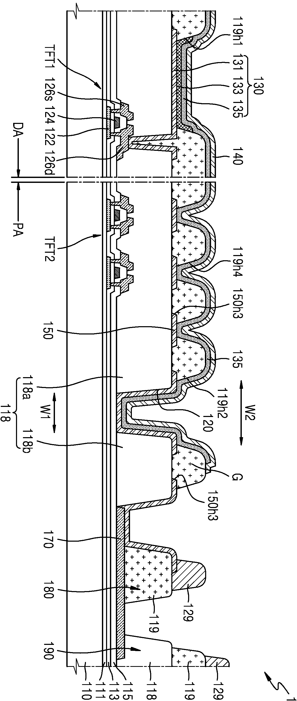
Of the present invention in the embodiment are organic light emitting display device relates to search, more specifically number Image the quality deteriorates during use positive or pore-organic light emitting device can reduce the door preventing or number are disclosed. Organic light emitting display device is an electron injection electrode electron injecting electrode formed therein between organic light-emitting layer including organic light emitting elements, hole injection electrode and the electrons injected an electron injection electrode formed in the main the electron (exciton) state (excited state) to OLEDs generated herein combine in the organic light emitting layer preferably dispersed from a light emitting element for generating light falls into (ground state) while display device are disclosed. A light emitting element and display device in organic light emitting display device is lightweight for monitoring low reverse separate light sources can be made thin, viewing angle, contrast (contrast), in the presence of a MP3 player or excellent response speed since back in television (TV) to expand up to the evacuator citation portable device and for a range of applications. However organic light emitting display device is or includes an inlet device, or device which is contained in the gas or moisture generated in the organic impurities such as organic light-emitting device to form a contact surface of the degradation during use door number number positive or pore-flow tides. The present invention refers to said door number points such as points provided for solving the various door number, arrangement according to number of the quality deteriorates door preventing or reducing the number of organic light emitting display device can be intended for a . Example number is however and generally, the range of the present invention is defined in which are not correct. According to one aspect of the present invention, substrate; said display area located on said display region and a peripheral region located; said display region and peripheral region is located, said valley separating insulating layer in the peripheral region with organic insulating layer number 1; in said display area, said number 1 organic insulating layer over the electrode located subsequent to number 1, number 2 light-emitting layer and one pixel electrode, said number 2 electrode includes a plurality of light-emitting layer and covering said valleys, a plurality of organic light-emitting device; said number 1 disposed on the organic insulating layer in said display region and peripheral region, said central portion opening exposing said number 1 electrode number 1 and number 2 including opening overlying the upper surface of the valleys, number 2 organic insulating layer; and said number 2 electrode has an area wider than said number 2 for covering the grow a layer; a organic light emitting display device including a number substrate. As one in the embodiment, is located on said peripheral region, said blue light emission power supply line further comprises a power supply, said power supply line can be said a display area and positioned between the valley. As one in the embodiment, is located on said peripheral region, said number 2 electrode power supply line connecting said number 1 can be the first package. As one in the embodiment, said conductive layer covering said longitudinally extending valley can be connected. As one in the embodiment, said conductive layer in said valley [khen it will choose be directly connected said number 2 electrode. As one in the embodiment, power supply line connected to said conductive layer can cover a portion of said number 1. As one in the embodiment, said material having an electrode conductive layer equal to said number 1 can be connected. As one in the embodiment, said organic insulating layer having a plurality of number 3 opening connected conductive layer said number 1 can be open. As one in the embodiment, said conductive layer having a plurality of number 4 opening connected said number 2 an organic insulating layer can be open. As one in the embodiment, said number 2 electrode is connected through an opening in said conductive layer be [khen it will choose said number 4. As one in the embodiment, the said valley are positioned to surround the display area can be. As one in the embodiment, is located on said peripheral area, in which the number 1 not overlap with the power supply line, said power supply further comprises a power supply line number 2 blue light emission can be. As one in the embodiment, the ends of the valley disposed outside of said reference electrode said number 2 said display area, said display area in the corners of the end of the valley formed at both ends of the distance between the other than said number 2 electrode materials disposed in the region of the edge area corresponding to a distance between the end of said number 2 electrode materials disposed valley may be less than disclosed. As one in the embodiment, said formed at both ends of the corners of the display area, the display area can be formed in said direction said valley. As one in the embodiment, the corners of the formed at both ends of said display area, said electrode is said number 2 can be projecting away from a display. As one in the embodiment, said it digs up, dizzily the layer can be organic. As one in the embodiment, said grow a layer positioned on a display area can be said sealing ring. By another aspect of the present invention the, substrate; positioned on said substrate, including a plurality of organic light-emitting display area; said display region located, organic insulating layers separating the valleys; said outer valleys located, said organic light-emitting device for supplying power to power supply lines; said outer power supply line located dam issue; and valley portion for covering said display area, said power supply line is connected to the common electrode of organic light-emitting; said common electrode has an area wider than said common electrode covering grow a layer; and said grow a layer positioned on, sealing member including at least one organic film and at least one inorganic layer; a organic light emitting display device including a number substrate. As one in the embodiment, is located on said display region, said power supply line connecting said common electrode can be the first package. As one in the embodiment, said sealing member of said display area and said organic layer can be located inside a display area facing said dam issue. As one in the embodiment, thin film sealing said display area and said inorganic layer is disposed to cover the dam issue can be an outwardly extending said dam issue. Said dam issue number 1 and number 2 can be located on the dam issue dam issue comprising said number 1 located dam issue. Another aspect of the aforementioned addition, feature, advantage embodiment of the invention hereinafter for specific content, will activitycopyright from claim and drawing. In the embodiment of the present invention according to one made as said, door number number of preventing or reducing the quality deteriorates during use or pore-forming process for organic light emitting display device can be implementing. This effect of the present invention as well as by time is are not correct. Figure 1 shows a one in the embodiment according to of the present invention also organic light emitting display device (1) to determine the portion of the shown plane are disclosed. Figure 2 shows a II a-II along the organic light emitting display device (1) to determine the part of cross-sectional drawing of Figure 1 shown are disclosed. Figure 3 shows a organic light emitting display device (1) sealing member is formed to shape cross-sectional drawing of Figure 2 shown are disclosed. Figure 4 shows a comparison example organic light emitting display device also according to (2) to determine the portion of the shown plane are disclosed. Figure 5 shows a V a-V along the organic light emitting display device (2) to determine the part of cross-sectional drawing of Figure 4 shown are disclosed. Figure 9 shows a 6 to organic light emitting display device according to an embodiment of the present invention may also (1) in, number 1 organic insulating layer (118) formed valley part (120), number 2 electrode (135), and grow a layer (140) to determine various design modification shown plane are disclosed. Figure 10 shows a one in the embodiment according to of the present invention also organic light emitting display device (3) to determine the portion of the shown plane are disclosed. Figure 11 shows a one in the embodiment according to of the present invention also organic light emitting display device (4) to determine the portion of the shown plane are disclosed. The present invention refers to conversion may have various in the embodiment can apply various bar, in the embodiment example are specific detailed description and drawing the broadcast receiver. The effect of the invention and features, achieving the drawing method in the embodiment and an electronic component connected to the reference surface with specifically carry activitycopyright will. In the embodiment in the present invention refers to hereinafter however are limited to rather than the disclosure can be implemented in various forms. Hereinafter, with reference to the attached drawing of the present invention in the embodiment for which is a detailed, with reference to the drawing described when determining the same components or corresponding local impart the drawing code description dispensed the on-sensors other. In the embodiment of layer in a hereinafter, film, region, other components such as plate components when it "on", "directly on" as well as any other components when interposed therebetween when other components comprises a unit. In addition to drawing or a reduced and apparatus for facilitating descriptions in near the components can be. For example, size and thickness of each configuration exhibited drawing representing a virtual path identifier arbitrarily for facilitating the descriptor, not limited to the present invention are not necessarily shown. Figure 1 shows a one in the embodiment according to of the present invention also organic light emitting display device (1) to determine the portion of the plane view and shown, Figure 2 shows a II a-II along the organic light emitting display device (1) to determine the portion of the shown cross-sectional drawing and, Figure 3 of Figure 2 organic light emitting display device (1) of Figure 1 shown in cross-section form and the sealing member is formed are disclosed. With reference also to the 3 1 also, in the embodiment according to one organic light emitting display device (1) of the substrate (110) and (DA) on display area, display area (DA) is located on the non-display area located peripheral area (PA) combined with each other. The outer display area (DA), planarization film serves organic insulating layer number 1 (118) separating the valleys (120) is formed on each pixel. Emitting organic insulating layer deposited on number 2 (119) is valley part (120) number 2 in opening (119h 2) is formed. The valleys (120) number 2 film is formed on a common electrode (135) the valley part (120) is located, grow a layer (140) is number 2 electrode (135) covering the substrate. In the in the embodiment, the valleys (120) formed about the number 2 electrode (135) and grow a layer (140) the structure of the organic light emitting display device (1) gas generated or moisture contained within the organic impurities such as extending into the servicing the device. In the embodiment hereinafter the organic light emitting display device of (1) a detailed as follows. Substrate (110) is glass material, can be made of a material such as various plastic or metal material. For example, substrate (110) is polyether sulfone (polyethersulphone, PES), polyacrylate (polyacrylate, PAR), polyether-imide (polyetherimide, PEI), polyethylene naphthalate (polyethyelenen napthalate, PEN), raid (polyethyeleneterepthalate, PET) polyethylene terephthalate, polyphenylene sulfide (polyphenylene sulfide, PPS), polyarylate (polyallylate), polyimide (polyimide, PI), polycarbonate (polycarbonate, PC) or cellulose acetate propionate (cellulose acetate propionate, CAP) be a polymer resin such as including a flexible substrate. (DA) as is possible displaying display area, a plurality of number 1 (TFT1) and a plurality of thin film transistor electrically connected to a plurality of organic light emitting thin film transistor (TFT1) number 1 (130) can be arranged. Number 1 (TFT1) thin film transistor substrate (110) between silicon oxide, method for forming metal wire such as inorganic material including the jade it is sour but sprout the id and/or silicon buffer layer (111) can be interposed. Buffer layer (111) substrate (110) the upper surface of the substrate is increased or the impurities centipoise (110) through semiconductor layer (122) can be crystallized and which serves for preventing or diminishing. Number 1 includes a thin film transistor (TFT1) amorphous silicon, polycrystalline silicon or organic semiconductor material including semiconductor layer (122), gate electrode (124), a source electrode (126s) and a drain electrode (126d) can be comprising. Semiconductor layer (122) part of the gate electrode (124) disposed thereon. Gate electrode (124) signal applied to the source electrode (126s) and a drain electrode (126d) electrically communication with each other. Gate electrode (124) is adhesion with an adjacent layer, surface flatness by considering processability and stacked layer, such as aluminum (Al), platinum (Pt), palladium (Pd), is (Ag), magnesium (Mg), gold (Au), nickel (Ni), neodymium (Nd), iridium (Ir), chromium (Cr), lithium (Li), calcium (Ca), molybdenum (Mo), titanium (Ti), tungsten (W), copper (Cu) to at least one of single or multi-layer can be formed. Semiconductor layer (122) and a floating gate electrode (124) in order to ensure the insulation between, silicon oxide, a silicon nitride and/or silicon such as inorganic substance from the jade it is sour but sprout the id including gate insulating film (113) semiconductor layer (122) and a floating gate electrode (124) can be interposed between. Gate electrode (124) part of the silicon oxide, a silicon nitride and/or silicon such as inorganic substance from the jade it is sour but sprout the id including an interlayer insulating film (115) is disposed, a source electrode (126s) and a drain electrode (126d) the interlayer insulating film (115) can be disposed on. A source electrode (126s) and a drain electrode (126d) is an interlayer insulating film (115) on a gate insulating film (113) through semiconductor layer formed on the underlayer (122) thereof are connected thereto. A source electrode (126s) and a drain electrode (126d) aluminum (Al), platinum (Pt), palladium (Pd), is (Ag), magnesium (Mg), gold (Au), nickel (Ni), neodymium (Nd), iridium (Ir), chromium (Cr), lithium (Li), calcium (Ca), molybdenum (Mo), titanium (Ti), tungsten (W), at least one of copper (Cu) single or multi-layer material can be formed. Substrate (110) can be positioned to be in the region of the thin film transistor (TFT2) (PA) number 2. Number 2 in the display area (DA) an electric signal applied to the thin film transistor (TFT2) for circuit number to be a part of. Such a thin film transistor (TFT2) number 1 number 2 is the magnetic circuit with the thin film transistor (TFT1) can be the same. In addition, thin film transistor (TFT2) number 1 number 2 is the magnetic circuit with the thin film transistor (TFT1) different from those disapproval. Such a thin film transistor (TFT1) number 1 number 2 thin film transistor (TFT2) is made of a material which can be the same. For example, thin film transistor (TFT2) number 2 is amorphous silicon, polycrystalline silicon or organic semiconductor material including semiconductor layer (not shown) can be include. In addition, thin film transistor (TFT2) number 1 number 2 on the thin film transistor (TFT1) can be formed of a different material. Thin film transistor (TFT1) number 1 number 1 on organic insulating layer (118) can be disposed. The organic light emitting thin film transistor (TFT1) number 1 (130) is when placed in, number 1 organic insulating layer (118) is by use of a planarization film electrode number 1 (131) is number 1 organic insulating layer (118) that is smooth with respect to the upper HL2. Number 1 organic insulating layer (118) for example acrylic, BCB (Benzocyclobutene), HMDSO (polyimide) or organic material such as polyimide (Hexamethyldisiloxane) can be formed. Number 1 in Figure 2 includes organic insulating layer (118) shown with but a single layer, a cured resin layer can be formed that a deformable disclosed. Number 1 organic insulating layer (118) and a peripheral region (PA) (DA) all gate lines are formed. , Number 1 organic insulating layer (118) in organic insulating layer surrounding regions (PA) number 1 (118) at least 2 regions (118a, 118b) physically separated into longitudinally extending valley (120) contact with each other. Valley part (120) is formed on the organic film cliff, organic insulating number 1 (118) through gas (G) or moisture from impurities such as display area (DA) from being transferred are shut off. In display area (DA), organic insulating layer number 1 (118) on, electrode number 1 (131), number 2 electrode (135) and interposed between a light-emitting layer including intermediate layer (133) having organic light-emitting device (130) is disposed thereon. Number 1 electrode (131) transparent electrode or reflective electrode can be formed. Number 1 electrode (131) when the transparent electrode formed can be a transparent conductive layer. (ITO: indium tin oxide) dielectric layer for producing cable indium, indium (IZO: indium zinc oxide), (ZnO: zinc oxide), indium oxide (In2O 3: indium oxide), indium gallium oxide (IGO: indium galium oxide), and aluminum (AZO: aluminium zinc oxide) can be at least any one selected from the group including a. In this case, for further includes a light-transparent conductive in addition can be bantu and layer, Ag bantu and layer to be formed of thin films of several tens of nm, Mg, Al, Pt, Pd, Au, Ni, Nd, Ir, Cr, Li, Ca, and Yb is at least one selected from the group including a can be. When Ag reflective electrode formed, Mg, Al, Pt, Pd, Au, Ni, Nd, Ir, Cr and combinations thereof and the like a reflection film, reflective film upper and/or can be arranged in a lower transparent conductive layer. A dielectric layer ITO, IZO, ZnO, In2O 3: indium oxide, IGO, and AZO including at least any one selected from the group a can be. The present invention is not limited to the electrode as well as number 1 (131) can be made of a variety, can be single or multi-layer structure in addition cured deformable disclosed. Number 1 organic insulating layer (118) on the display region and a peripheral region (PA) number 2 (DA) over organic insulating layer (119) can be disposed. Number 1 electrode (131) exposing a central portion of the organic insulating layer number 2 (119) number 1 of opening (119h 1) defining pixel values could be bonded each other. In addition, organic insulating layer number 2 (119) is electrode number 1 (131) covers the edge of the, electrode number 1 (131) in the edges of the arc generation in can. Organic insulating layer number 2 (119) polyimide (PI; polyimide) or HMDSO (hexamethyldisiloxane) such as organic material can be formed. Organic insulating layer number 2 (119) number 1 the organic insulating layer (118) can be equal to or comprises different materials. Organic insulating layer number 2 (119) in organic insulating layer surrounding regions (PA) number 1 (118) formed valley part (120) opening exposing number 2 (119h 2) contact with each other. Opening number 2 (119h 2) number 1 includes organic insulating layer (118) formed valley part (120) in the same manner as organic layer by forming on cliff, number 2 organic insulating layer (119) through gas (G) or moisture from impurities such as display area (DA) from being transferred are shut off. Organic light-emitting device (130) intermediate (133) can be is a mineral or polymer material. Intermediate layer (133) when the low molecular weight material, an intermediate layer (133) hole injection layer (HIL: Hole Injection Layer), a hole transport layer (HTL: Hole Transport Layer), (EML: Emission Layer) light-emitting layer, an electron transport layer (ETL: Electron Transport Layer), like unitary or composite structure of the metal layer (EIL: Electron Injection Layer) be a laminated structure. Intermediate layer (133) copper phthalocyanine (CuPc: copper phthalocyanine), N, N - di (naphthalene - 1 - yl) - N, N'- diphenyl - benzidine (N, N' - Di (naphthalene-a 1 a-yl) - N, N' - diphenyl-a benzidine: NPB), tris - 8 - hydroxyquinoline aluminum (tris-a 8 a-hydroxyquinoline aluminum) (Alq3) various organic material can be a virtual channel. Intermediate layer (133) such as the vacuum deposition method can be formed. Intermediate layer (133) there is usually a hole transport layer (HTL) polymer material and including a light emitting layer (EML) may have structure. At this time, a hole transport layer comprising PEDOT, the light emitting layer such as PPV (Poly-a Phenylenevinylene) systems and polyfluorenes (Polyfluorene) based can be at a. This intermediate layer (133) is screen printing or inkjet printing method, fabrication method (LITI; Laser induced thermal imaging) method such as can be formed. Intermediate layer (133) comprises a plurality of electrode number 1 (131) may be integral across layer, a plurality of number 1 electrode (131) so as to correspond to each patterned layers may be filled. Number 2 electrode (135) the display area (DA) and a peripheral zone (PA) formed over. Intermediate layer (133) and number 2 organic insulating layer (119) of, number 2 organic insulating layer (119) number 2 of opening (119h 2) of, and number 1 organic insulating layer (118) of the valleys (120) can be positioned inside the bulb. Number 2 electrode (135) comprises a plurality of organic light-emitting device (130) and to the integrated (bodies) as common electrode are formed a plurality of number 1 electrode (131) may correspond to be. Number 2 electrode (135) transparent electrode or reflective electrode can be formed. Number 2 electrode (135) when formed into the transparent electrode is Ag, Al, Mg, Li, Ca, Cu, LiF/Ca, LiF/Al, MgAg and CaAg can be selected from one or more material, having a thickness of several tens of nm to be can be a thin film shape. Number 2 electrode (135) when the reflective electrode formed Ag, Al, Mg, Li, Ca, Cu, LiF/Ca, LiF/Al, MgAg CaAg and selected from the group including a surface plasmon can be. Number 2 as well as electrode (135) and multi-material is not limited to various deformable body are disclosed. Number 2 electrode (135) upper light emitting element to improve efficiency in protecting grow a layer (140) is combined with each other. Grow a layer (140) and a light emitting element such as a protecting layer for improving the optical efficiency can be formed in a plurality of layers. For example, grow a layer (140) in order to improve the electron beam silicon oxide (SiO2), silicon nitride (SiNx), zinc oxide (ZnO2), titanium oxide (TiO2), zirconium oxide (ZrO2), indium tin oxide (ITO), indium zinc oxide (IZO), Alq3, CuPc, CBP, a-a NPB, and at least one of comprising ZiO2 can be organic or inorganic. In other in the embodiment, grow a layer (140) the organic (30) for generating surface plasmon resonance light can be provided to the user. For example, grow a layer (140) can be nano-particles. On the other hand, grow a layer (140) is sealing member (160) for forming chemical vapor deposition (Chemical Vapor Disposition: CVD) process or sputtering (sputtering) process heat, plasma (plasma) by organic light-emitting device (130) to prevent damage to the can. For example, grow a layer (140) can be practiced (bisphenol) epoxy (epoxy) resin, epoxidized butadiene (butadiene) resin, fluorene (fluorine) of at least one of epoxy resin-base epoxy resin for simultaneous (novolac) can be epoxy-based materials. In the embodiment the in grow a layer (140) is number 2 electrode (135) cover both number 2 electrode end of a jacket (135) is greater than the area of the form. Grow a layer (140) is number 2 electrode (135) over the without, sealing member (160) chemical vapor deposition process or sputtering process for forming when, number 2 electrode (135) to prevent the resultant to tame. The organic matter including grow a layer (140) can be diffuse display device for moisture or gas passage. According to the various aberrations in the embodiment, number 2 electrode (135) formed in the spacer (DA) device and displayed through the organic insulating layer in a direction towards the number 1 (118) formed valley part (120) and extending, valley part (120) number 2 on the outside of the organic insulating layer (190) number 2 formed opening (119h 2) extends to disposed thereon. The, number 1 organic insulating layer (118) or number 2 organic insulating layer (119) gas (G) in moisture or number 2 electrode (135) by closes grow a layer (140) can be prevent diffusion of the impurities as determined by. Specifically, a comparison module also 4 and also 5 through a browser substrate. Figure 4 shows a comparison example organic light emitting display device also according to (2) to determine and shown in plane view, Figure 5 shows a V a-V along the organic light emitting display device (2) to determine the portion of the cross-section of Figure 4 shown are disclosed. The same reference number comprises the above-described in the embodiment exhibits the same components. In the embodiment described above about the empty described substrate. The reference also 4 and 5 also, organic light emitting display device embodiments of comparison (2) electrode in number 2 (235) the valley part (120) display panel (DA) facing inner to the lungs. Embodiments of organic light emitting display device comparison (2) organic insulating layer even number 1 (118) in organic insulating layer surrounding regions (PA) number 1 (118) at least 2 regions (118a, 118b) physically separated into longitudinally extending valley (120) contact with each other. Valley part (120) is formed on the organic film cliff, number 1 organic insulating layer (118) through gas (G) or moisture from impurities such as sounding an alarm to shut off. Even comparison example, organic insulating layer number 2 (119) in organic insulating layer surrounding regions (PA) number 1 (118) formed valley part (120) opening exposing number 2 (119h 2) contact with each other. Opening number 2 (119h 2) number 1 includes organic insulating layer (118) formed valley part (120) in the same manner as organic layer by forming on cliff, number 2 organic insulating layer (119) through gas (G) or moisture from impurities such as sounding an alarm to shut off. But, in comparison, a common electrode number 2 electrode (235) the valley part (120) towards the display panel and located inside, number 2 electrode (235) to grow a layer (140) and for the cover. Grow a layer (140) the valley part (120) when located outside, number 1 organic insulating layer (118) or number 2 organic insulating layer (119) gas (G) diffuse through electrode is number 2 (235) without interrupted by, organic matter including grow a layer (140) can be spread along. Grow a layer (140) gas (G) is diffused along the valleys (120) number 1 inside the organic insulating layer (118) and number 2 organic insulating layer (119) then transferred. The delivered gas (G) or water (DA) impurities such as the display area such that multi (130) can be causes degradation in a. However, the number 2 in the embodiment in electrode (135, also reference 2) number 1 above display device in a direction towards the organic insulating layer (118) formed valley part (120) and extending, valley part (120) number 2 on the outside of the organic insulating layer (190) number 2 of opening (119h 2) extends to form source, grow a layer (140) number 1 through organic insulating layer (118) or number 2 organic insulating layer (119) of the cylinder spread to tame. Try to grow a layer (140) diffuses through the even number 2 electrode (135) organic light emitting element (130) so that the organic light emitting device and second cover thereof can. With reference also to the 3 1 also again, peripheral area (PA) of the valleys (120) on the outer organic light-emitting device (130) for supplying power to the power supply line number 1 (170) and number 2 power supply line (171) is the lungs. Number 1 power supply line (170) is a low-voltage supply (ELVSS) implementation being. Power supply line number 1 (170) comprises a connecting conductive layer (150) number 2 through electrode (135) connected, organic light-emitting device (130) low-voltage applies power. Power supply line number 1 (170) can be provided to surround the display area (DA) about. In the embodiment number 1 in a power supply line (170) the display area (DA) around 'some' real-shown surrounded by U-shaped structure, the present invention refers to is not limited. Power supply line number 1 (170) the display area such that either side can be hydroxyl (DA). Number 2 power supply line (171) is a low-voltage supply (ELVSS) implementation being. Number 2 power supply line (171) (DA) direct display area is connected to the organic light emitting device (130) applies power high voltage. Organic light-emitting device (130) includes a power supply line number 1 (170) and number 2 power supply line (171) (PAD) used for connecting portion out through the power supply device can be connected. Organic insulating layer disposed peripheral area (PA) number 1 (118) of the upper and the valleys (120) of the connecting conductive layer (150) can be disposed. Connected conductive layer (150) is electrode number 1 (131) being disposed in the same layer, connected conductive layer (150) number 1 at least a portion of organic insulating layer (118) and number 2 organic insulating layer (119) can be disposed between. Connected conductive layer (150) is electrode number 1 (131) is formed of the same material as, the valleys (120) can be a completely covers. According to one in the embodiment, connected conductive layer (150) is valley part (120) opening situated on the perimeter of a plurality of number 3 (150h 3) include, number 2 organic insulating layer (119) comprises a connecting conductive layer (150) opening exposing at least a portion of number 4 (119h 4) can be include. Organic insulating layer number 2 (119) number 4 is opening (119h 4) can be separated into a plurality of regions by. Connected conductive layer (150) number 3 included in opening (150h 3) are, connected conductive layer (150) is arranged below the organic material number 1 organic insulating layer (118) can be emitted to the outside from the function as gas passages. Number 1 through organic insulating layer (118) from the gas domains (DA) in order to organic light emitting display device (1) is bent in arrangement according to prevent or reduce the number can be a door. Organic insulating layer number 2 (119) number 4 of opening (119h 4) is connected to conductive layer (150) expose, number 2 organic insulating layer (119) disposed on number 2 electrode (135) opening the number 4 (119h 4) connected via a conductive layer (150) and [khen it will choose be. Connected conductive layer (150) is number 2 electrode (135) number 1 for supplying power to the power supply line (170) and connected thereto. Number 1 organic insulating layer (118) formed valley part (120) is (DA) can be positioned to surround the display area. In the embodiment in a valley part (120) includes a display area (DA) around 'some' real-shown surrounded by U-shaped structure, the present invention refers to is not limited. Number 1 organic insulating layer (118) is the valleys (120) about the number 1 region (118a) and number 2 region (118b) can be physically separated spatially. Similarly number 2 organic insulating layer (119) is valley part (120) located opening corresponds to number 2 (119h 2) can be separated by at least 2 regions. Organic insulating layer number 2 (119) number 2 included in opening (119h 2) number 1 (W2) is the width of organic insulating layer (118) included in the valleys (120) can be greater than the width of (W1). The valley part (120) number 2 pair of organic insulating layer (119) disposed may not disclosed. Connected conductive layer (150) also can be positioned to surround the peripheral area (PA) display panel (DA), the valleys (120) can be cover. Connected conductive layer (150) is valley part (120) formed in the vicinity of opening a plurality of number 3 (150h 3) can be include. Number 2 electrode (135) the display area (DA) and a peripheral zone (PA) which is disposed along, the valleys (120) thereof can fully cover. Number 2 electrode (135) the valley part (120) in the interior of the connected conductive layer (150) can be in direct contact with. On the other hand, connected conductive layer (150) a portion of the valley part (120) without fully covering, connected conductive layer (150) number 1 another portion of organic insulating layer (118) and number 2 organic insulating layer (119) can be disposed between. In addition, connected conductive layer (150) is valley part (120) part of disapproval. However, even when the conductive layer (150) the display area (DA) over the region surrounding the valley part (120) covering at least part of should. The reference also 3, grow a layer (140) on at least one inorganic film and at least one organic layer including sealing member (160) can be arranged. Sealing member (160) includes a display area (DA) peripheral region extending covers (PA) can be. This sealing member (160) is also shown in an inorganic layer 3 such as number 1 (161), organic layer (163) and an inorganic layer number 2 (165) can be comprising. An inorganic layer number 1 (161) is grow a layer (140) that covers, silicon oxide, a silicon nitride and/or silicon can be like the jade it is sour but sprout the id. It is an inorganic layer number 1 (161) and grow a layer (140) including LiF layer (not shown) or the like interposed between the disapproval. An inorganic layer number 1 (161) is formed along to lower structure, such as a first substrate 3 also shown in upper surface thereof can. Organic layer (163) that are the inorganic layer number 1 (161) covering, organic layer (163) a substantially planar top surface of the can. Organic layer (163) polyethylene terephthalate, polyethylene naphthalate, polycarbonate, polyimide, polyethylene sulfonate, polyoxymethylene, polyarylate, polyacrylate process can be selected from the group consisting the methyl d thread rock it buys one or more materials. An inorganic layer number 2 (165) organic layer (163) that covers, silicon oxide, a silicon nitride and/or silicon can be like the jade it is sour but sprout the id. Triazines shown but, inorganic layer number 2 (165) the organic light emitting device (1) number 1 in its edge area of an inorganic layer (161) contained by, organic layer (163) to display device can be separated from the die. The sealing member (160) is an inorganic layer number 1 (161), organic layer (163) and an inorganic layer number 2 (165) including a bar, the multilayer structure and a sealing member (160) even if that cracks in, an inorganic layer number 1 (161) and organic layer (163) between or organic layer (163) and an inorganic layer number 2 (165) can be interconnected between to cracks. The spacer (DA) such as moisture or oxygen from the outside through the lower electrode is formed on the path capable of preventing or diminishing. Power supply line number 1 (170) and number 2 power supply line (171) outside dam issue number 1 (180) and dam issue number 2 (190) is the lungs. Of Figure 1 plane view is not shown but, dam issue number 1 (180) and dam issue number 2 (190) is formed to surround the display area (DA) can be. Dam issue number 1 (180) and dam issue number 2 (190) is an organic layer (163) servicing the peripheral area (PA) from leaking phenomenon. Dam issue number 1 (180) is number 2 organic insulating layer (119) and a spacer (129) be a laminated structure. However, not limited to the present invention refers to, dam issue number 1 (180) is number 2 organic insulating layer (119) and spacer (129) and the other material, different heights can be formed. For example, dam issue number 1 (180) is number 1 organic insulating layer (118) and number 2 organic insulating layer (119) be a structure formed by a. Dam issue number 2 (190) is number 1 organic insulating layer (118), organic insulating layer number 2 (119) and spacer (129) be a stacked structure. However, not limited to the present invention refers to, dam issue number 2 (190) is number 1 organic insulating layer (118), organic insulating layer number 2 (119) and spacer (129) and the other material, different heights can be formed. Dam issue number 2 (190) number 1 of organic insulating layer (118) is number 1 power supply line (170) by covering the end of the, heat or medicines to a backplane (backplane) used during process for preparing number number 1 power supply line (170) can be encoded. Dam issue number 2 (190) is an organic layer (163) (PA) peripheral region as well as to prevent leaking, sealing member (160) in number forming process for preparing, metal mask (not shown) during use of the metal mask is number 2 electrode (135) can be plotted surface of the cover. 1 To 3 also shown but not detailed, spacer (129) includes a sealing member (160) process for preparing metal mask (not shown) forming in number during use of the metal mask is number 2 electrode (135) provided reference pattern including a surface of, display area (DA) and a peripheral zone (DA) can be formed in a portion of. Figure 9 shows a 6 to organic light emitting display device according to an embodiment of the present invention may also (1) in, organic insulating number 1 (118) formed valley part (120), number 2 electrode (135), and grow a layer (140) to determine various design modification shown plane are disclosed. 6 Also reference surface, the valleys (120) is viewed in a plane round edge region can be formed. Number 2 electrode (135) the valley part (120) and a completely covers, grow a layer (140) is number 2 electrode (135) completely covers the substrate. In the in the embodiment, display area (DA) formed at both ends of electrode edge region of number 2 (135) end of the valley part (120) is the distance between a region (d2), e.g. display area (DA) formed at both ends of sides of number 2 electrode (135) end of the valley part (120) (d1) distance between such as disclosed. The reference also 7, valley part (120) is viewed in a plane perpendicular edge region can be formed. Number 2 electrode (135) the valley part (120) and a completely covers, grow a layer (140) is number 2 electrode (135) completely covers the substrate. In the in the embodiment, display area (DA) formed at both ends of electrode edge region of number 2 (135) end of the valley part (120) is the distance between a region (d4), e.g. display area (DA) formed at both ends of sides of number 2 electrode (135) end of the valley part (120) (d3) distance between may be less than disclosed. The reference also 8, valley part (120) is viewed in a plane can be composed of fine patterned region. I.e., valley part (120) is "L" can be user form fine patterned region. Number 2 electrode (135) the valley part (120) and a completely covers, grow a layer (140) is number 2 electrode (135) completely covers the substrate. In the in the embodiment, display area (DA) formed at both ends of electrode edge region of number 2 (135) end of the valley part (120) is the distance between a region (d6), e.g. display area (DA) formed at both ends of sides of number 2 electrode (135) end of the valley part (120) can be greater than the distance between the (d5). The reference also 9, valley part (120) is viewed in a plane patterned electrode number 2 (135) the spacer can be protrudes upwardly away from the region. Number 2 electrode (135) the valley part (120) and a completely covers, grow a layer (140) is number 2 electrode (135) completely covers the substrate. In the in the embodiment, display area (DA) formed at both ends of electrode edge region of number 2 (135) end of the valley part (120) is the distance between a region (d8), e.g. display area (DA) formed at both ends of sides of number 2 electrode (135) end of the valley part (120) (d7) distance between less than or may be bigger. To changes in the above-mentioned hole are 6 design of Figure 9, number 2 electrode (135) can be optimizing edges. In addition number 2 electrode (135) by optimizing electrode edges number 2 (135) which completely covers grow a layer (140) can be optimizing edges. Number 2 electrode (135) and grow a layer (140) by optimizing edges, or for optimizing the design of materials used in the upper peripheral region (PA) can. In the embodiment according to Figure 10 shows a of the present invention also other organic light emitting display device (3) to determine the portion of the shown plane are disclosed. Organic light emitting display device of Figure 10 (3) organic light emitting display device of Figure 3 is (1) a non-organic insulating layer number 2 taught (319) and number 2 electrode (335) is used to structure of flow tides. The number 2 in the embodiment of organic insulating layer (319) of Figure 3 the organic light emitting display device (1) unlike on, connected conductive layer (150) to expose the upper surface of an opening (119h 4, also reference 2) does not form a. The, electrode number 2 (335) is number 2 organic insulating layer (319) connected via an opening formed conductive layer (150) and not contact. Number 2 organic insulating layer (319) a portion of the surface, electrode through an opening number 2 (335) formed organic insulating layer until number 2 (319) for discharging gas generated in that instead, which form openings in accomplishing patterning process. Thus, the matters in the embodiment gas to the interests of the diffusion barrier layer to divide the but the gain of 1. Figure 11 shows a of the present invention also in the embodiment according to another organic light emitting display device (4) to determine the portion of the shown plane are disclosed. Organic light emitting display device of Figure 11 (4) of Figure 10 is organic light emitting display device (3) when compared to the connected conductive layer (450) is used to structure of flow tides. Connected conductive layer (450) opening (150h 3, also 10 reference) patterning process does not forming organic light emitting display device of Figure 10 (3) in the embodiment of process for preparing a number of device number can be more easily the high pressure liquid coolant. In the embodiment are organic light emitting display device according to the above (1, 3, 4) organic insulating layer in the peripheral region (PA) organic film formed longitudinally extending valley cliff number 1, number 2 common electrodes disposed externally of the valley part electrode prevents diffusion of impurities by applying a can. In addition, capping electrode number 2 is greater than the number 2 electrode completely covers to the same thickness as that by preventing the oxidation of the electrode can be electrically connected with the number 2. In the embodiment shown in the present invention refers to drawing the reference only to an exemplary is at a radiates heat and, if the art therefrom in various deformation and equally to the other person with skill in the art will understand that it is in the embodiment. The technical idea of the present invention defined by appended claim of true technology protection range generated by the will. 1: Organic light emitting display device DA: display area PA: peripheral region TFT1: number 1 thin film transistor TFT2: number 2 thin film transistor 110: Substrate 111: Buffer layer 113: Gate insulating film 115: Interlayer insulating film 118: Number 1 organic insulating layer 119: Number 2 organic insulating layer 120: Valley part 130: Organic light emitting device 131: Number 1 electrode 133: Intermediate layer 135: Number 2 electrode 140: Grow a layer 150: Connected conductive layer 160: Sealing member 170: Power supply line number 1 171: Power supply line number 2 180: Dam issue number 1 190: Dam issue number 2 The present invention provides an organic light emitting display device having a structure capable of preventing or reducing problem of degradation of image quality. The organic light emitting display device comprises: a substrate; a display region positioned on the substrate and a peripheral region positioned at the outer display region; a first organic insulating layer positioned at the display region and the peripheral region and having a valley unit separating the insulating layer in the peripheral region; a plurality of organic light emitting devices including a first electrode, a light emitting layer, and a second electrode sequentially positioned on the first organic insulating layer in the display region, wherein the second electrode cover a plurality of light emitting layers and the valley unit; a second organic insulating layer disposed on the first organic insulating layer in the display region and the peripheral region and including a first opening exposing the central part of the first electrode and a second opening overlapping the valley unit; and a capping layer covering the second electrode with a larger area than the second electrode. COPYRIGHT KIPO 2018 Substrate; and said display area located on said display region and a peripheral region located; said display region and peripheral region is located, said valley separating insulating layer in the peripheral region with organic insulating layer number 1; in said display area, said number 1 organic insulating layer over the electrode located subsequent to number 1, number 2 light-emitting layer and one pixel electrode, said number 2 electrode includes a plurality of light-emitting layer and covering said longitudinally extending valley, a plurality of organic light-emitting device; said number 1 disposed on the organic insulating layer in said display region and peripheral region, said central portion opening exposing said number 1 electrode number 1 and number 2 including opening overlying the upper surface of the valleys, number 2 organic insulating layer; and said number 2 electrode has an area wider than said number 2 for covering the grow a layer; including the organic light emitting display device. According to Claim 1, which is mounted on said peripheral area, said blue light emission number 1 (ELVSS) power supply line further comprises a power supply, said power supply line located between the number 1 a display area and said valley organic light emitting device. According to Claim 2, is located on said peripheral region, said number 2 electrode power supply line connecting said number 1 further including conductive layer organic light emitting display device. According to Claim 3, said longitudinally extending valley cover connected to said conductive layer organic light emitting device. According to Claim 4, said conductive layer in said organic light emitting display device connected valley said number 2 electrode contact directly. According to Claim 3, cover a portion of said number 1 power supply line connected to said conductive layer organic light emitting device. According to Claim 3, organic light emitting display device including the same material connected to said conductive layer and said number 1. According to Claim 3, said organic insulating layer having a plurality of number 3 connected conductive layer based on the organic light emitting display device including opening said number 1. According to Claim 8, said number 2 an organic insulating layer including a plurality of number 4 opening open layer having a symmetrical to said organic light emitting display device. According to Claim 8, said number 2 electrode is connected through an opening in said conductive layer contact the organic light emitting display device said number 4. According to Claim 1, said organic light emitting display device said valley portion is provided so as to surround a part of display area. According to Claim 1, which is mounted on said peripheral area, said number 1 not overlap with certain lock located power supply line, said power supply further including blue light emission organic light emitting display device power supply line number 2. According to Claim 12, the ends of the valley disposed outside of said reference electrode said number 2 said display area, said display area in the corners of the end of the valley formed at both ends of the distance between the other than said number 2 electrode materials disposed in the region of the edge area corresponding to a distance between the end of the valley is less than said number 2 electrode materials disposed, organic light emitting display device. According to Claim 12, said formed at both ends of the corners of the display area, the display area added said direction said valley, organic light emitting display device. According to Claim 12, said formed at both ends of the corners of the display area, said number 2 that engages said electrode is away from a display, organic light emitting display device. According to Claim 1, said organic matter it digs up, dizzily the layer including organic light emitting display device. According to Claim 1, said sealing member including said grow a layer positioned on a display area further, organic light emitting display device. Substrate; positioned on said substrate, including a plurality of organic light-emitting display area; said display region located, organic insulating layers separating the valleys; said outer valleys located, said organic light-emitting device for supplying power to power supply lines; said outer power supply line located dam issue; and valley portion for covering said display area, said power supply line connected to the common electrode of an organic light emitting devices; said common electrode has an area wider than said common electrode covering grow a layer; and said grow a layer positioned on, and at least one inorganic layer including at least one organic film sealing member; including a organic light emitting display device. According to Claim 18, which is mounted on said display region, said conductive layer including the common electrode power supply line connecting said further organic light emitting display device. According to Claim 18, said sealing member located inside said display area and said organic layer of said organic light emitting device display area facing dam issue. According to Claim 18, said display area and said inorganic layer is disposed to cover the thin film sealing dam issue, said outwardly extending dam issue organic light emitting display device. According to Claim 18, said dam issue number 1 and number 2 located on the organic light emitting display device including said number 1 dam issue dam issue located dam issue.