MANUFACTURING METHOD OF ARRAY SUBSTRATE
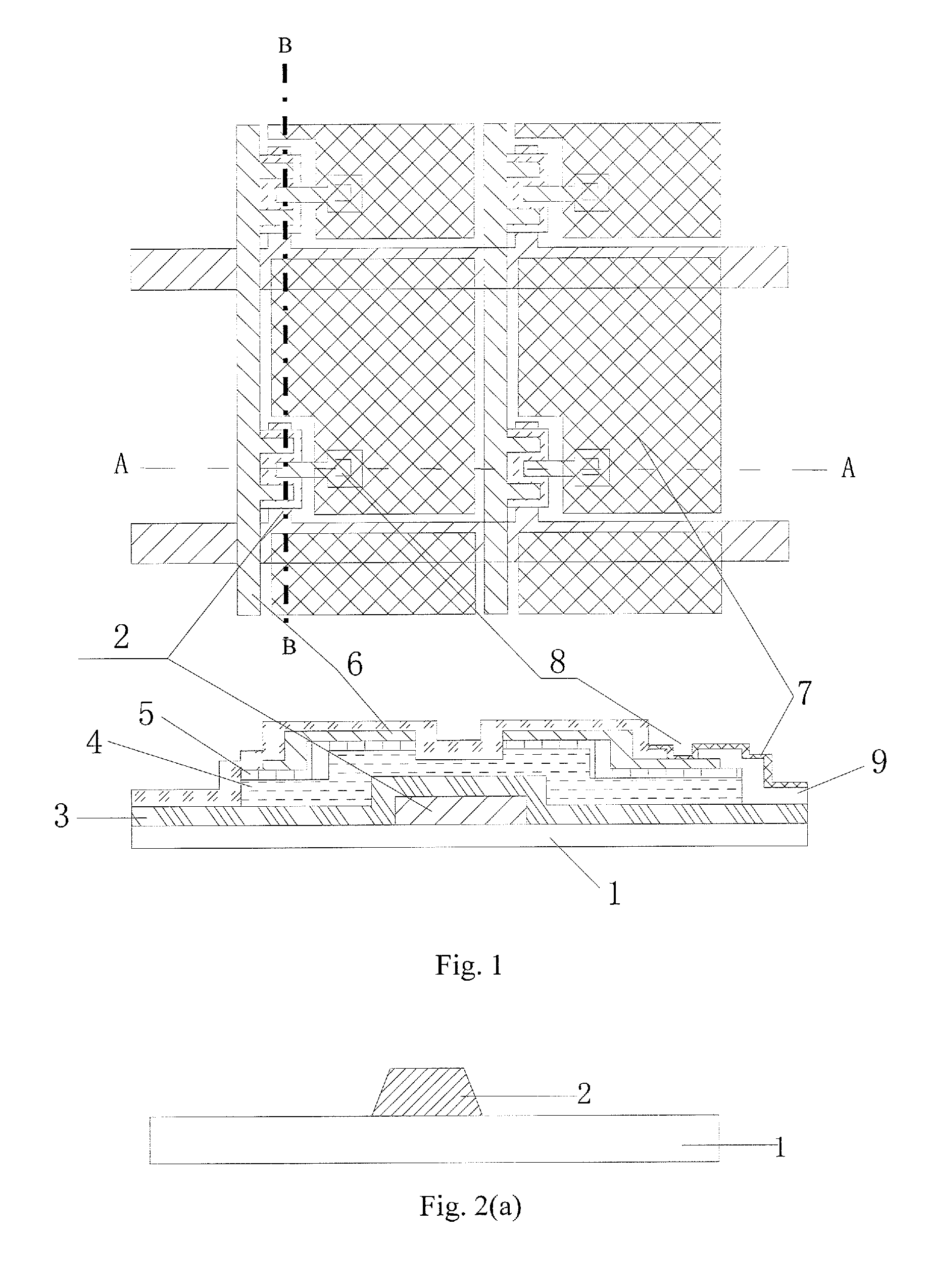
Embodiments of the disclosed technology relate to a manufacturing method of an array substrate. TFT-LCDs have many advantages, such as small volume, low power consumption and non-radiation, and have dominated the current flat panel display market. A TFT-LCD is formed by bonding an array substrate and a color filter substrate. As shown in (1) depositing a gate metal film on a glass substrate 1, and forming a gate signal line (not shown) and a gate electrode 2 by using a gate mask, as shown in (2) successively depositing a gate insulation layer 3, an amorphous silicon thin film 4, an ohmic contact layer 5 and a metal layer 6 on the glass substrate 1 after the step (1), and forming a photoresist pattern by an exposure through a grey tone mask and a development process, and removing the redundant parts of the active layer, the metal layer 6 and the photoresist through multiple etching processes so as to form a data line, source/drain electrodes 6, and a channel between the source and drain electrodes, as shown in (3) depositing a thin film for forming a passivation layer 9 on the substrate 1 after the step (2), and forming a passivation layer via hole 8 in a portion of the passivation layer which located above the drain electrode by performing a masking and etching process on the passivation layer 9, as shown in (4) depositing an ITO electrode layer on the substrate after the step (3), and forming a pixel electrode 7 by using an ITO mask, and the pixel electrode 7 is connected with the drain electrode through the passivation layer via hole 8, as shown in The multiple etching processes in the step (2) are as follows in detail: firstly, removing most of the metal layer outside the pixel region by a first wet etching, as shown in The multiple etching processes are complex and needs a long period of time. Generally, a gas mixture of SF6and O2, which has a relatively large etching rate on the photoresist but small etching rate on the active layer, is used to ash the photoresist. In addition, a gas mixture composed of SF6and Cl2, which has a relatively large etching rate on the active layer but small etching rate on the photoresist, is used in etching the active layer. The gas mixture has a relatively higher etching rate on the gate insulation layer at the lower part, so that the gate insulation layer is etched so much and an uneven embossing mura is caused. This unevenness may have influence on the product quality after a module is formed. Furthermore, in the multiple etching process of the conventional 4-mask process, the active layer is etched for forming the active layer pattern before the photoresist is ashed for exposing the channel region, and thus a relatively large amount of active layer wing (also called active layer tail) is remained at the two sides of the data line and the two sides of the TFT region (including the source/drain regions and the channel region), as shown by “h1” in An embodiment of the disclosed technology provides a manufacturing method of an array substrate, comprising the following steps: S1. forming a gate signal line and a gate electrode on a base substrate, successively depositing a gate insulating layer, an active layer, and a metal layer, forming a photoresist pattern on the metal layer, and removing the metal layer outside a region for Ruining a data line, a channel and source/drain electrodes with the photoresist pattern as an etching mask; S2. simultaneously etching the active layer outside the region for forming the data line, the channel and the source/drain electrodes and ashing the photoresist so as to expose the metal layer within a channel region; S3. removing the metal layer within the channel region by performing a wet etch or a dry etch so as to form the source/drain electrodes; S4. removing a part of the active layer within the channel region so as to form the channel; and S5. depositing a passivation layer on the base substrate after the step S4, and forming a passivation layer via hole in the passivation layer above the drain electrode; depositing a transparent pixel electrode layer, and forming a pixel electrode which is connected with the drain electrode through the passivation layer via hole. Further scope of applicability of the disclosed technology will become apparent from the detailed description given hereinafter. However, it should be understood that the detailed description and specific examples, while indicating preferred embodiments of the disclosed technology, are given by way of illustration only, since various changes and modifications within the spirit and scope of the disclosed technology will become apparent to those skilled in the art from the following detailed description. The disclosed technology will become more fully understood from the detailed description given hereinafter and the accompanying drawings which are given by way of illustration only, and thus are not limitative of the disclosed technology and wherein: Embodiments of the disclosed technology now will be described more clearly and fully hereinafter with reference to the accompanying drawings, in which the embodiments of the disclosed technology are shown. Apparently, only some embodiments of the disclosed technology, but not all of embodiments, are set forth here, and the disclosed technology may be embodied in other forms. All of other embodiments made by those skilled in the art based on embodiments disclosed herein without mental work fall within the scope of the disclosed technology. The manufacturing method of a thin film transistor liquid crystal display (TFT-LCD) array substrate according to the disclosed technology is described in detail as follows by taking in conjunction with the accompany figures and embodiments. In addition, the array substrate manufacturing by the method according to the embodiments of the disclosed technology has a similar configuration as shown in S1, forming a gate electrode signal line and a gate electrode on a base substrate (for example, a glass substrate) 1, successively depositing a gate insulating layer (not shown), an active layer (for example, including an amorphous silicon layer 4 and an ohmic contact layer 5), and a metal layer 6; forming a photoresist pattern by performing a exposure and development process through a gray tone mask or a half tone mask (the structure after the development process is shown in S2, simultaneously etching the active layer outside the region for fanning the data line, the channel and the source/drain electrodes and ashing the photoresist so as to expose the metal layer 6 within the channel region. As shown in In the step of S2, a gas mixture of SF6, O2and Cl2is used. As for this gas mixture, it can have a relatively large etching rate on both the photoresist and the active layer by adjusting the content of each gas therein. Alternatively, the SF6in the above gas mixture can be replaced by other gas containing fluorine such as CF4; and the Cl2can be replaced by other gas containing chlorine such as CH3Cl. In addition, after the step S2, a certain thickness of active layer outside the region for forming the data line, the channel and the source/drain electrodes is remained, and this layer of the residual active layer can protect the underlying gate insulating layer from being etched by the above gas mixture. S2-1, performing an etching with a large etching rate on the residual active layer outside the region for forming the data line, the channel and the source/drain electrodes and a part of photoresist on the substrate after the step S2, so as to remove the entire of the residual active layer outside the region for forming the data line, the channel and the source/drain electrodes and a part of the photoresist 10. In this step, the etching rate on the active layer is relatively larger comparing with that in the step 2. Moreover, as shown in S3, performing a second wet etch or a dry etch on the substrate 1 after the step S2-1 so as to remove the metal layer 6 within the channel region and form the source/drain electrodes, as shown in S4, removing a part of the active layer within the channel region by a N+ etching so as to form a channel, as shown in S5, depositing a passivation layer on the substrate 1 after the step S5 and forming a passivation layer via hole in the portion corresponding to the drain electrode; depositing a ITO electrode layer, and forming a ITO electrode (pixel electrode) which is connected with the drain electrode through the passivation layer via hole. The above mentioned step S1 may comprise the following steps: S1.1, depositing a gate metal thin film on the base substrate 1, and forming the gate signal line and the gate electrode by a patterning process; the patterning process may comprises the steps such as photoresist applying, exposure, development, and etching; S1.2, successively depositing the gate insulating layer, the active layer composed of the amorphous silicon layer 4 and the ohmic contact layer 5, and the metal layer 6, and forming the photoresist pattern by performing the exposure and development process by using a gray tone mask or a half tone mask, as shown in S1.3, removing the part of the metal layer 6 outside the region for forming the data line, the channel and the source/drain electrodes by using a wet etching, as shown in In the above mentioned step S5, forming the pixel electrode may comprise depositing an ITO electrode layer after forming the passivation layer and the via hole therein, forming the ITO electrode by using an ITO mask, and the ITO electrode and the drain electrode being connected through the passivation layer via hole. The SDT etching is performed by two steps of dry etch in the steps S2 and S2.1, and its total time is shorter than that in the 4-mask process of the prior art. For example, the processing time for these steps is reduced by 40-70 seconds, which improves the yield. On the substrate after the step S2.1, the width “h2” of the active layer wing at both sides of the data line is reduced comparing with the width “h1” in the prior art, thus the boundary of the ITO pattern (i.e., the ITO electrode) can be shifted in a direction towards the data line; thus, the space between the adjacent ITO patterns is reduced and the aperture ratio is enhanced. In addition, the amount of the active layer wing (the part extends beyond the data line) is reduced, i.e., the width of the active layer under the data line is reduced, for example, by about 0.5-1.0 μm for each side, which can improves the design quality and the product quality. In addition, no defectiveness will occur in the two dry etch processes of the steps S2 and S2.1, which avoids the occurrence of unevenness of embossing mura. In addition, the width “h2” of the active layer wing at the two sides of the TFT region is shorter than the “h1” (as shown in A1, forming a gate electrode signal line and a gate electrode on a base substrate (for example, a glass substrate) 1, successively depositing a gate insulating layer (not shown), an active layer (for example, including an amorphous silicon layer 4 and an ohmic contact layer 5), and a metal layer 6; forming a photoresist pattern by performing a exposure and development process through a gray tone mask or a half tone mask (the structure after the development process is shown in A2, simultaneously etching the active layer outside the region for forming the data line, the channel and the source/drain electrodes and ashing the photoresist so as to expose the metal layer 6 within the channel region. As shown in In the step of A2, a gas mixture of SF6, O2and Cl2is used. As for this gas mixture, it can have a relatively large etching rate on both the photoresist and the active layer by adjusting the content of each gas therein. Alternatively, the SF6in the above gas mixture can be replaced by other gas containing fluorine such as CF4; and the Cl2can be replaced by other gas containing chlorine such as CH3Cl. In addition, after the step A2, a certain thickness of active layer outside the region for forming the data line, the channel and the source/drain electrodes is remained, and this layer of the residual active layer can protect the underlying gate insulating layer from being etched by the above gas mixture. A3, performing a second wet etch or a dry etch on the substrate 1 after the step A2 so as to remove the metal layer 6 within the channel region and form the source/drain electrodes, as shown in A4, removing a part of the active layer within the channel through a N+ etch to form the channel, and simultaneously removing the residual active layer outside the region for forming the data line, the channel and the source/drain electrodes (a second active layer etching), as shown in A5, depositing a passivation layer on the substrate 1 after the step S5 and forming a passivation layer via hole in the portion corresponding to the drain electrode; depositing a ITO electrode layer, forming a ITO electrode (pixel electrode) which is connected with the drain electrode through the passivation layer via hole. The thickness of the residual active layer after the step A2 is about 300-800 Å, and the residual active layer will be etched when performing the step A4. Generally, during the N+ etch in the step A4, the active layer within the channel will be etched by about 1000-1300 Å in thickness, so as to guarantee the residual active layer of 300-800 Å to be etched in the step A4 and an over-etch for ensuring the uniformity of the large substrate. Compared with the method of the first embodiment, the method of the present embodiment is further simplified, saves the time for etching the residual active layer. Meanwhile, the switching time from the step S2 to the step S2-1 in the method of the first embodiment is omitted, and the yield can be enhanced. In addition, the width “h3” (as shown in B1, forming a gate electrode signal line and a gate electrode on a base substrate (for example, a glass substrate) 1, successively depositing a gate insulating layer (not shown), an active layer (for example, including an amorphous silicon layer 4 and an ohmic contact layer 5), and a metal layer 6; forming a photoresist pattern by performing a exposure and development process through a gray tone mask or a half tone mask (the structure after the development process is shown in B2, simultaneously etching the active layer outside the region for forming the data line, the channel and the source/drain electrodes and ashing the photoresist so as to expose the metal layer 6 within the channel region. As shown in In the step of B2, a gas mixture of SF6, O2and Cl2is used. As for this gas mixture, it can have a relatively large etching rate on both the photoresist and the active layer by adjusting the content of each gas therein. Alternatively, the SF6in the above gas mixture can be replaced by other gas containing fluorine such as CF4; and the Cl2can be replaced by other gas containing chlorine such as CH3Cl. In addition, after the step B2, a certain thickness of active layer outside the region for forming the data line, the channel and the source/drain electrodes is remained, and this layer of the residual active layer can protect the underlying gate insulating layer from being etched by the above gas mixture. B3, performing a second wet etch or a dry etch on the substrate 1 after the step B2 so as to remove the metal layer 6 within the channel region and form the source/drain electrodes, simultaneously etching the residual active layer outside the region for forming the data line, the channel and the source/drain electrodes (a second active layer etching), as shown in B4, removing a part of the active layer within the channel region by a N+ etching so as to form a channel, as shown in B5, depositing a passivation layer on the substrate 1 after the step S5 and forming a passivation layer via hole in the portion corresponding to the drain electrode; depositing a ITO electrode layer, forming a ITO electrode (pixel electrode) which is connected with the drain electrode through the passivation layer via hole. The thickness of the residual active layer after performing the step B2 is about 200-500 Å, and the residual active layer will be etched when performing the step B3. The step B3 is mainly used to remove the metal layer within the channel region, and it may have a relatively large etching rate on the metal layer and a relatively small etching rate on the active layer for ensuring a uniformity of etching. Similar to the method of the second embodiment, the method of the present embodiment is further simplified, which saves the time of separately performing the second active layer etching to etch the residual active layer. Meanwhile, the switching time from the step S2 to the step S2-1 in the method of the first embodiment is omitted, and the yield can be enhanced. In addition, the width “h4” (as shown in In the various embodiments of the disclosed technology, for the convenience of illustration, a thin film transistor (TFT) with “U” shaped channel structure is taken as an example. However, the disclosed technology is not limited thereto, a TFT with “-” shaped type channel structure or other possible structures can also be used. Moreover, in the various embodiments of the disclosed technology, although a method for manufacturing a TN type array substrate is taken as an example to explain the technical solution, the technical solutions of the various embodiments of the disclosed technology are also be applicable in manufacturing array substrates of other types, for example, an array substrates of other types such as FFS (Fringe Field Switch) type, IPS (In Plane Switch) type, and etc. The manufacturing method of the TFT-LCD array substrate described in the various embodiments of the disclosed technology may be not only applied in manufacturing the conventional TFT-LCD array substrate, but also applied in manufacturing an array substrate of electronic paper and a back plate of OLED (Organic Light Emitting Display); thus, the array substrate in the various embodiments of the disclosed technology adopts a generalized conception, which comprises TFT-LCD array substrate, array substrate of electronic paper and back plate of OLED. It should be noted that the above embodiments only have the purpose of illustrating the disclosed technology, but not limiting it. Although the disclosed technology has been described with reference to the above embodiment, those skilled in the art should understand that modifications or alternations can be made to the solution or the technical feature in the described embodiments without departing from the spirit and scope of the disclosed technology. A manufacturing method of an array substrate, comprising the following steps: S1 forming a gate signal line and a gate electrode on a base substrate, successively depositing a gate insulating layer, an active layer, and a metal layer, faulting a mask formed of photoresist on the metal layer, and removing the metal layer outside a region for forming a data line and source/drain electrodes through the mask; S2. simultaneously etching the active layer and ashing the photoresist so as to expose the metal layer within a channel region; S3. etching the active layer exposed by the photoresist after being ashed after the step S2; S4. removing the metal layer within the channel region. 1. A manufacturing method of an array substrate, comprising the following steps:
S1. forming a gate signal line and a gate electrode on a base substrate, successively depositing a gate insulating layer, an active layer, and a metal layer, forming a photoresist pattern on the metal layer, and removing the metal layer outside a region for forming a data line, a channel and source/drain electrodes with the photoresist pattern as an etching mask; S2. simultaneously etching the active layer outside the region for forming the data line, the channel and the source/drain electrodes and ashing the photoresist so as to expose the metal layer within a channel region; S3. removing the metal layer within the channel region by performing a wet etch or a dry etch so as to form the source/drain electrodes; S4. removing a part of the active layer within the channel region so as to form the channel; and S5. depositing a passivation layer on the base substrate after the step S4, forming a passivation layer via hole in the passivation layer above the drain electrode; depositing a transparent pixel electrode layer, and forming a pixel electrode which is connected with the drain electrode through the passivation layer via hole. 2. The method of 3. The method of S2-1, etching the certain thickness of active layer remained outside the region for forming the data line, the channel and the source/drain electrodes and a part of photoresist on the base substrate after the step S2 so as to remove the certain thickness of active layer. 4. The method of 5. The method of 6. The method of S1.1, depositing a gate metal film on the base substrate, and forming the gate signal line and the gate electrode by a patterning process; S1.2, successively depositing the gate insulating layer, an amorphous silicon layer, an ohmic contact layer, and the metal layer, and forming the photoresist pattern on the metal layer, wherein the amorphous silicon layer and the ohmic contact layer constitute the active layer; and S1.3, removing the part of the metal layer outside the region for forming the data line, the channel and the source/drain electrodes by using a wet etching. 7. The method of 8. The method of 9. The method of 10. The method of 11. The method of depositing an indium tin oxide (ITO) layer on the base substrate formed with the passivation layer and the passivation layer via hole, patterning the ITO layer so as to form the pixel electrode. 12. The method of forming a layer of photoresist on the metal layer; exposing the photoresist through a grey tone mask or a half tone mask; and developing the photoresist after being exposed so as to form the photoresist pattern. 13. The method of 14. The method of 15. The method of BACKGROUND
SUMMARY
BRIEF DESCRIPTION OF DRAWINGS
DETAILED DESCRIPTION
First Embodiment
Second Embodiment
Third Embodiment