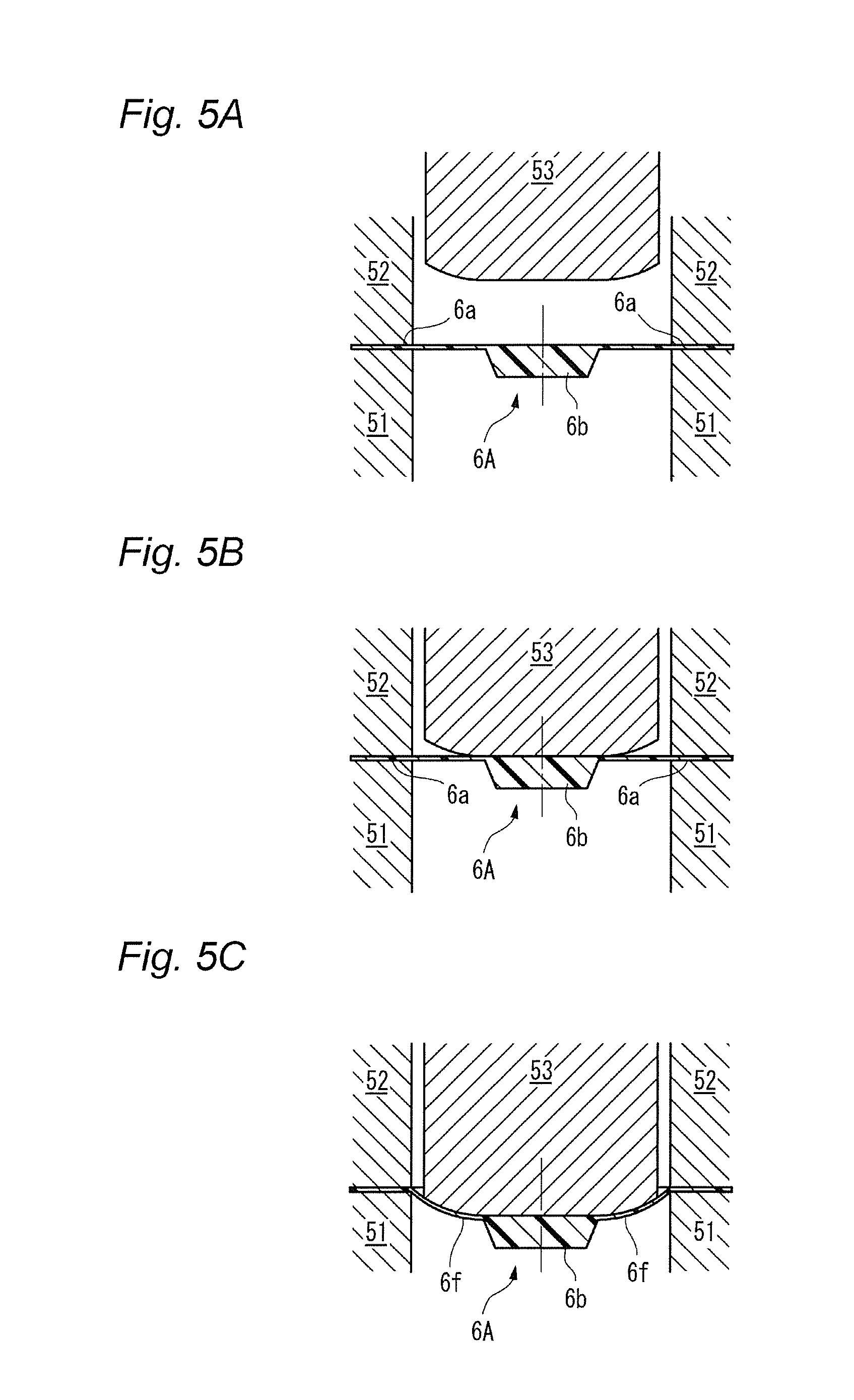
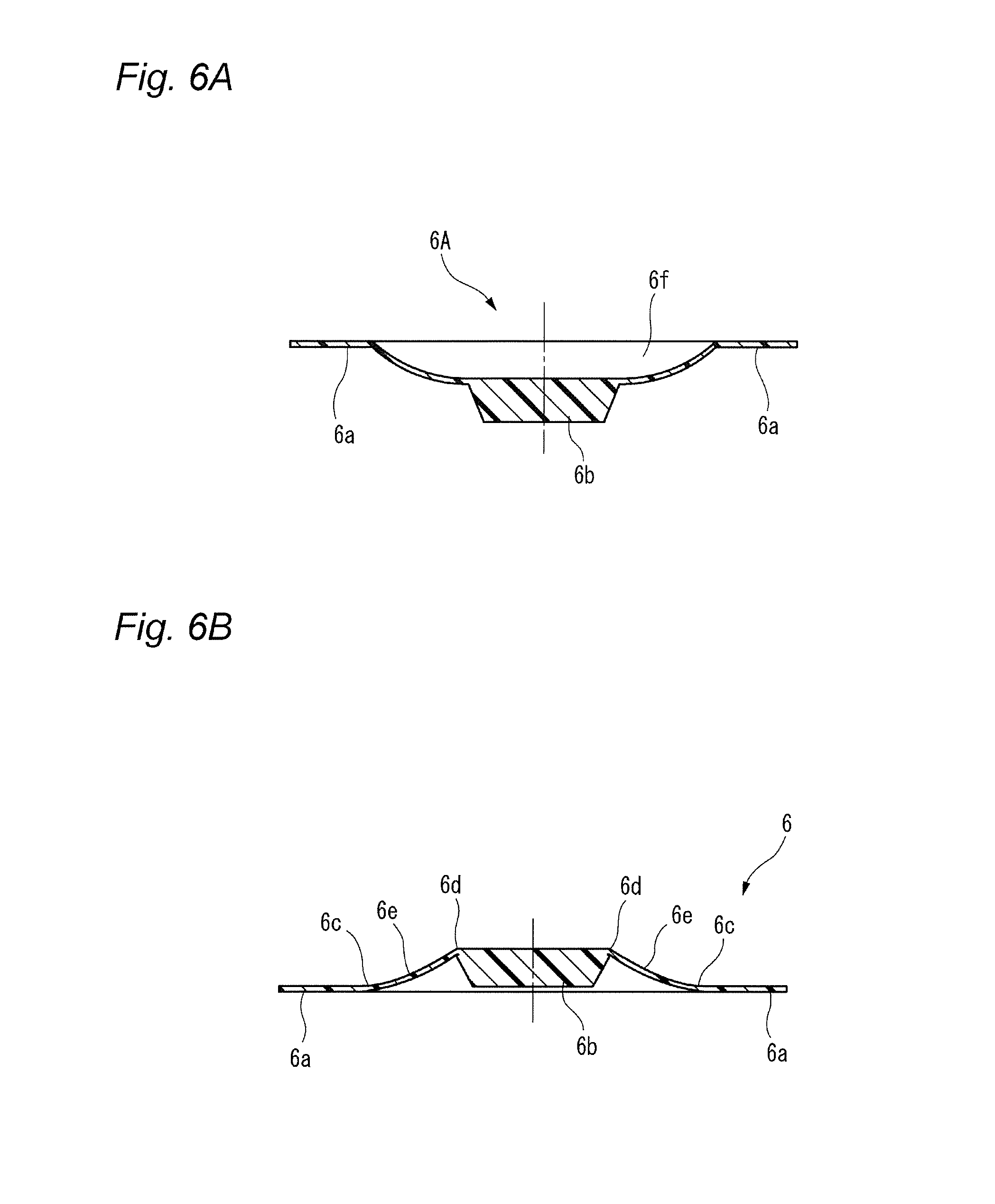
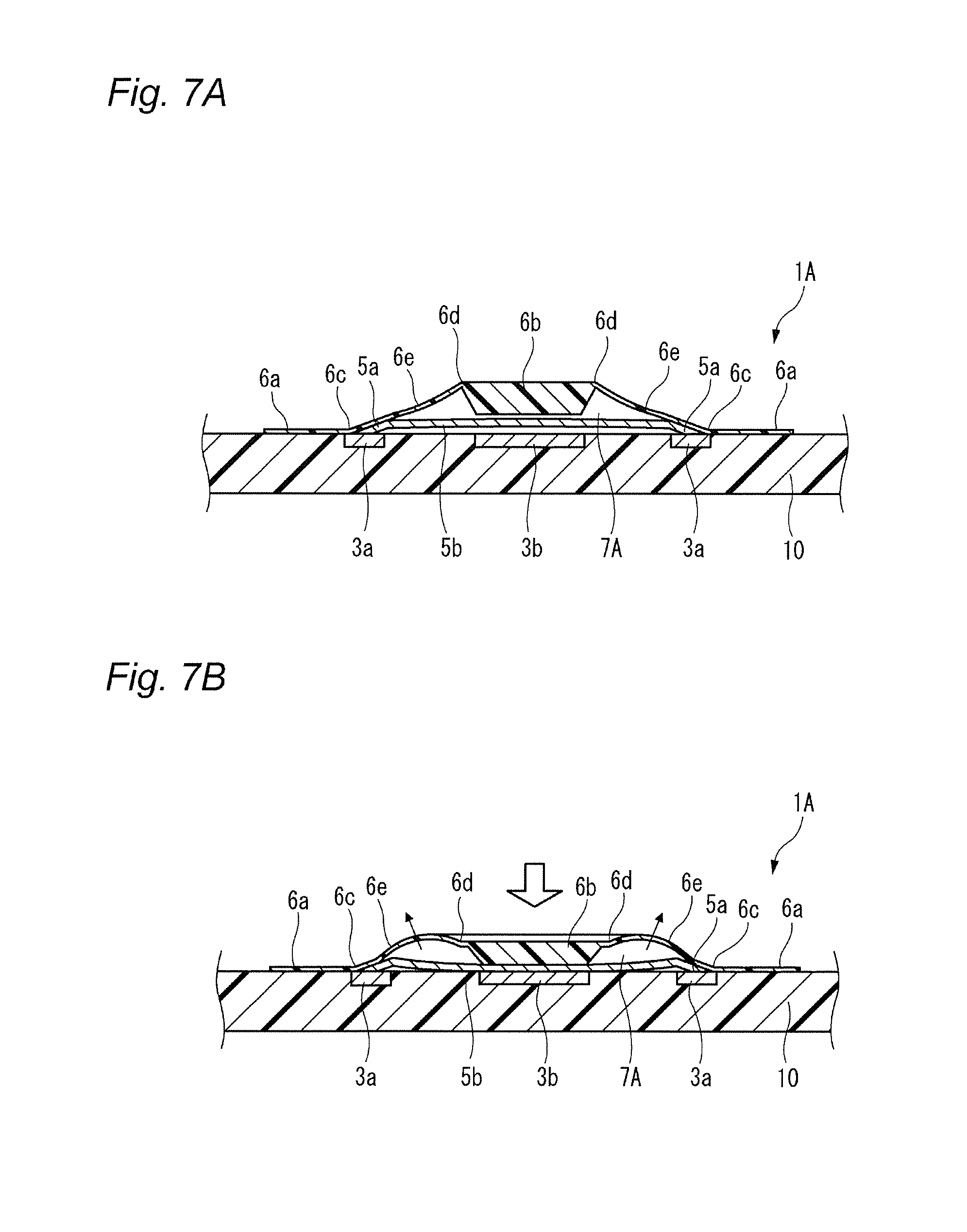
Switch and Manufacturing Method of Switch
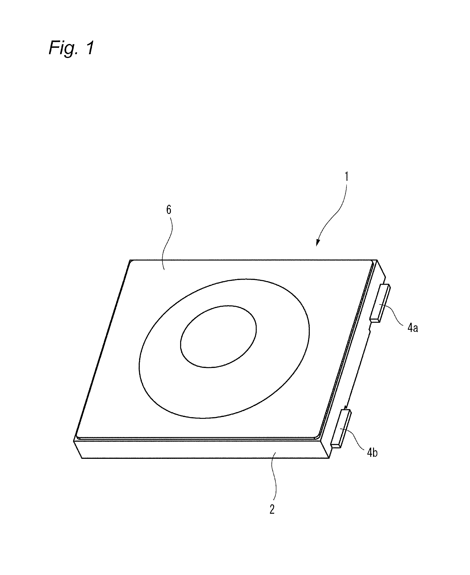
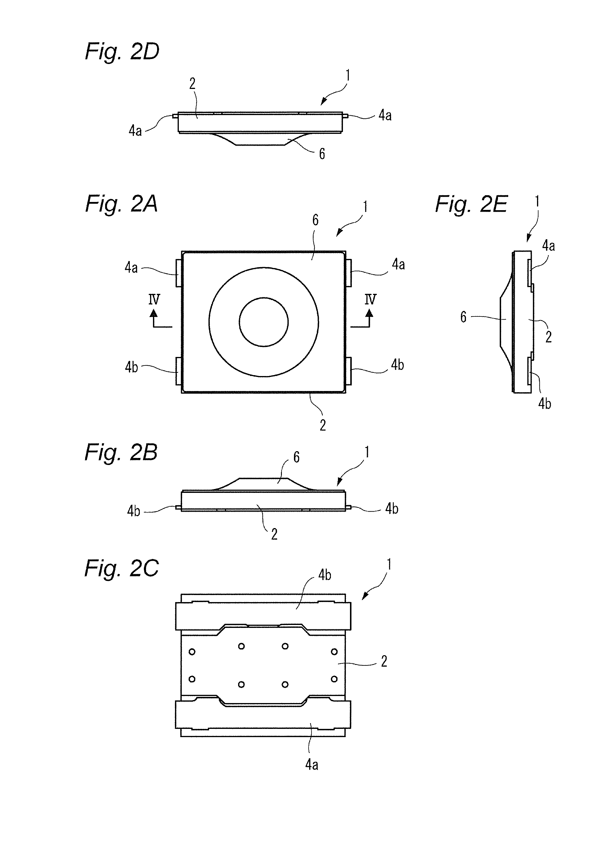
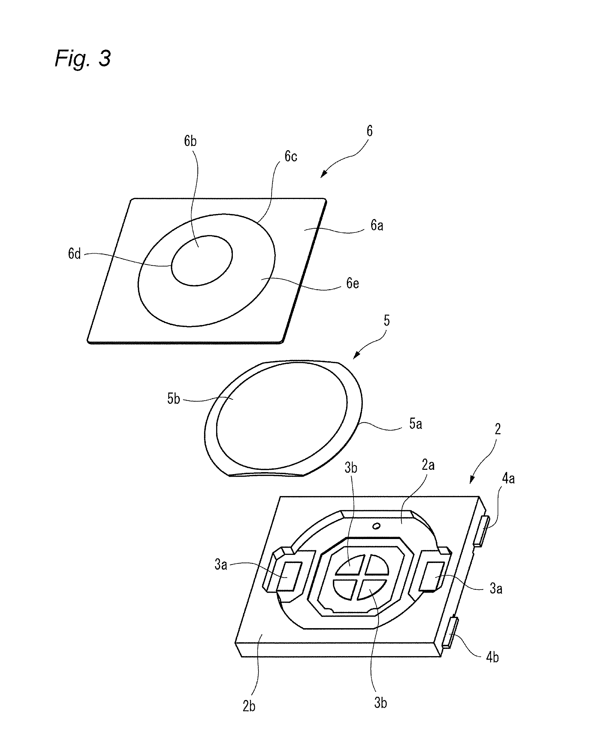
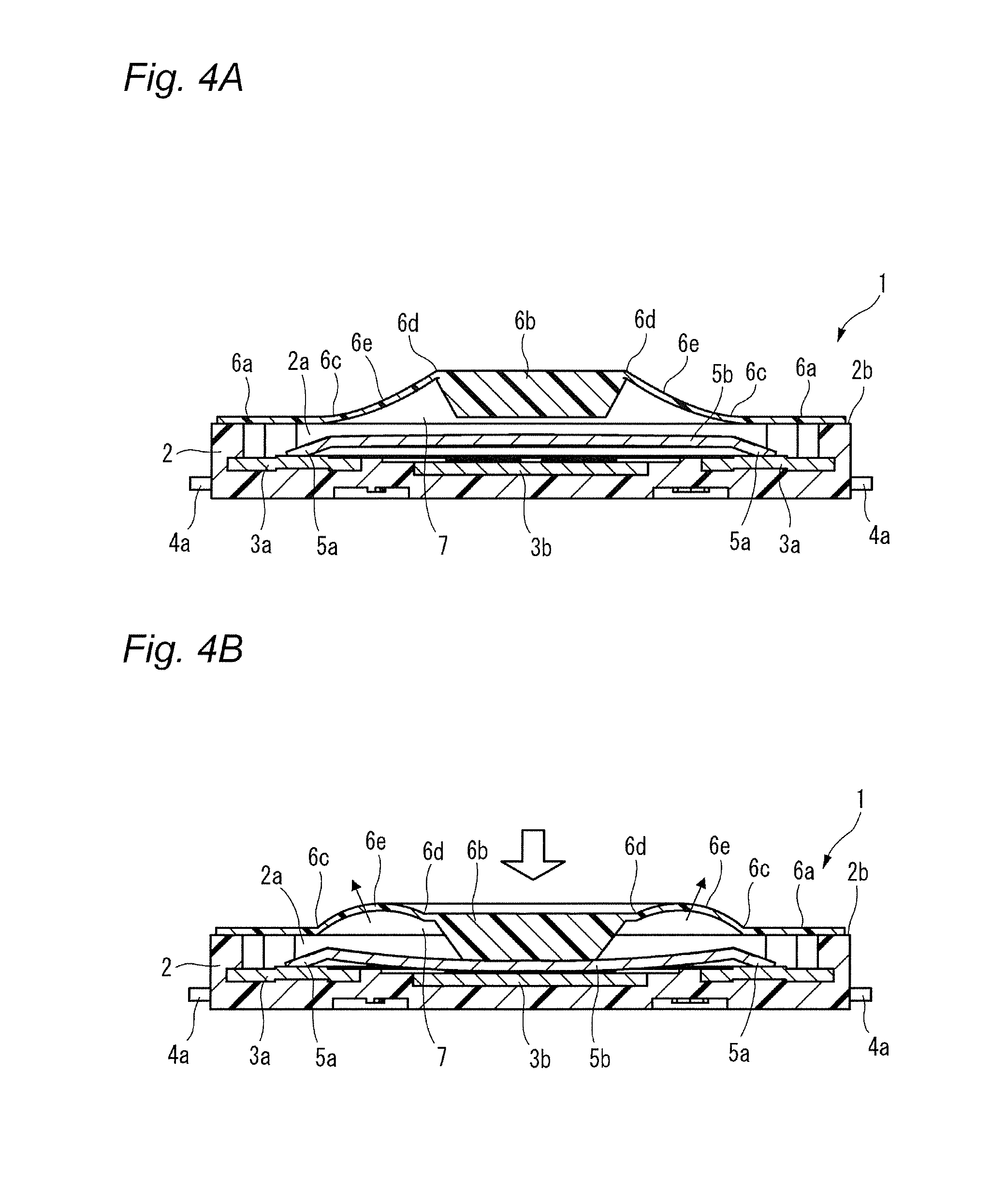
The present invention relates to a switch used in various small electronic devices, and particularly to a push switch mounted on a circuit board. Also, the invention relates to a manufacturing method of the switch. In this kind of apparatus, plural fixed electrodes and a movable electrode are arranged on a circuit board. The movable electrode can be elastically displaced between a first position in which the plural mutual fixed electrodes are in a conductive state and a second position in which the plural mutual fixed electrodes are in a non-conductive state, and a pressing member is arranged as opposed to the movable electrode in the second position at neutral state. When the pressing member displaces the movable electrode to the first position by a pressing force from the outside, the mutual fixed electrodes are changed to the conductive state. When the pressing force is released, the movable electrode elastically returns to the second position and the mutual fixed electrodes are changed to the non-conductive state (for example, see Patent Reference 1). [Patent Reference 1] JP-A-2009-123655 It is therefore one advantageous aspect of the present invention to provide a technique capable of obtaining a desired switch operational feeling even in the case of increasing hermeticity of space for storage of a movable electrode and a fixed electrode. According to one aspect of the invention, there is provided a switch comprising: a case, configured to be mounted on a circuit board, and including a recess; a plurality of fixed electrodes arranged inside the recess; a movable electrode, arranged inside the recess, and configured to be displaced between a first position in which the fixed electrodes are in a conductive state and a second position in which the fixed electrodes are in a non-conductive state; and a pressing member, arranged so as to cover at least a part of the recess, and configured to displace the movable electrode from the second position to the first position by a pressing force from the outside, wherein the pressing member includes a first bent part and a second bent part, and a deforming part disposed between the first bent part and the second bent part, the deforming part is opposed to the movable electrode with a gap in a state where the movable electrode is in the second position, and the deforming part is configured to be flexibly deformed toward the outside of the case in a state where the movable electrode is in the first position. The deforming part may be curved toward the outside of the case in the state where the movable electrode is in the first position. The deforming part may be curved toward the recess in the state where the movable electrode is in the second position. According to another aspect of the invention, there is provided a switch comprising: a circuit board; a plurality of fixed electrodes arranged on the circuit board; a movable electrode, configured to be displaced between a first position in which the fixed electrodes are in a conductive state and a second position in which the fixed electrodes are in a non-conductive state; and a pressing member, arranged on the circuit board, covering the fixed electrodes and the movable electrode, and configured to displace the movable electrode from the second position to the first position by a pressing force from the outside, wherein the pressing member includes a first bent part and a second bent part, and a deforming part disposed between the first bent part and the second bent part, the deforming part is opposed to the movable electrode with a gap in a state where the movable electrode is in the second position, and the deforming part is configured to be flexibly deformed in a direction away from the circuit board in a state where the movable electrode is in the first position. The deforming part may be curved in the direction away from the circuit board in the state where the movable electrode is in the first position. The deforming part may be curved toward the circuit board in the state where the movable electrode is in the second position. According to another aspect of the invention, there is provided a manufacturing method of a switch, comprising: holding a resin molded body by a plurality of dies; pressing the resin molded body from a first side thereof using a punch to form a plastic deformed part projecting to a second side opposite to the first side; deforming the plastic deformed part so as to project to the first side to form a first bent part and a second bent part; and arranging a part of the resin molded body disposed between the first bent part and the second bent part so as to be opposed to a movable electrode of the switch with a gap. The resin molded body may be formed of a material containing a thermosetting resin or a thermoplastic resin. It is necessary to increase hermeticity of space for storage of the movable electrode and the fixed electrodes based on requests for waterproofness and dustproofness. In this case, when the pressing force is depressed and the movable electrode is displaced toward the fixed electrode, the air present in the space is resistant to being deflated (or cannot be deflated), and acts as resistance to displacement of the pressing force. As a result, a desired switch operational feeling cannot be obtained. It is therefore one advantageous aspect of the present invention to provide a technique capable of obtaining a desired switch operational feeling even in the case of increasing hermeticity of space for storage of a movable electrode and a fixed electrode. Embodiments of the invention will hereinafter be described in detail with reference to the accompanying drawings. In addition, in each of the drawings used in the following description, a scale is properly changed in order to obtain the size capable of recognizing each member. As a first embodiment of a switch according to the invention, a perspective view of a push switch 1 is shown in As shown in these drawings, the push switch 1 has an external appearance in which a pressing member 6 is installed on an upper surface of a case 2 made of an insulating resin mounted on a circuit board. As shown in an exploded perspective view of Each of the first fixed electrodes 3 A movable electrode 5 is stored inside the recess 2 The pressing member 6 is arranged on the upper surface 2 The central part 5 The first fixed electrodes 3 That is, the movable electrode 5 can be displaced between a first position in which the plural mutual fixed electrodes 3 The pressing member 6 is made of materials containing a thermosetting resin or a thermoplastic resin such as a fluorine resin, a PEEK (polyether ether ketone) resin or polyimide. Since these materials have heat resistance, the materials are useful in the case of using reflow processing in soldering at the time of mounting the push switch 1 on the circuit board. A peripheral edge part 6 The pressing member 6 includes a press part 6 The pressing member 6 further includes a first bent part 6 The portion located in the radial outside of the first bent part 6 A part of the pressing member 6 sandwiched between the first bent part 6 The inclined part 6 When the pressing member 6 is pressed downwardly with operation of a button (not shown) etc., the press part 6 In the present embodiment, the inclined part 6 Consequently, even in a configuration in which hermeticity of the operation space 7 must be increased by requests for dustproofness and waterproofness, a desired switch operational feeling can be obtained without reducing operability of the pressing member 6. Next, a manufacturing method of the pressing member 6 will be described with reference to Next, as shown in With this deformation, a first bent part 6 In addition, the upper surface (first side) of the pressing member 6 has an indentation produced by pressing the punch 53. This indentation can show one of the circumstantial evidences that the above manufacturing method with the drawing processing is implemented. In addition, it is not always necessary to integrally mold the press part 6 Next, a push switch 1A according to a second embodiment of the invention will hereinafter be described with reference to A configuration of the push switch 1A according to the present embodiment differs that of the push switch 1 according to the first embodiment in that a peripheral edge part 6 As shown in The pressing member 6 is arranged on the circuit board 10 so as to cover the first fixed electrodes 3 In the present embodiment, operation space 7A of the movable electrode 5 is demarcated by directly gluing or welding the pressing member 6 to the circuit board 10, so that there is a tendency to increase hermeticity. Consequently, when the movable electrode 5 is displaced toward the circuit board 10, air which present inside the operation space 7A acts as resistance to operation of the pressing member 6. This resistance acts on an inclined part 6 Consequently, even in the push switch 1A having a structure with a tendency to increase hermeticity of the operation space 7A, a desired switch operational feeling can be obtained without reducing operability of the pressing member 6. The embodiments described above are means for facilitating understanding of the invention, and do not limit the invention. The invention can be changed or improved without departing from the gist of the invention and also, the invention naturally includes equivalents of the invention. In the push switch 1 (1A), it is not always necessary to curve the inclined part 6 In the push switch 1 (1A), it is not always necessary to curve the inclined part 6 Representation of the “upper side” and the “lower side” in the description described above is only used for convenience in the description with reference to the drawings, and does not intend to limit directions at the time of using a product. The “upper side” and the “lower side” can be translated into the “direction away from the circuit board” and the “direction near to the circuit board”, respectively. The shape and the number of press parts 6 The shapes of the first bent part 6 The movable electrode 5 can adopt proper shapes and configurations as long as the movable electrode 5 can be displaced from a position in which the plural mutual fixed electrodes are changed to a non-conductive state to a position in which the plural mutual fixed electrodes are changed to a conductive state by the pressing member 6. It is not always necessary to have elasticity. According to the present invention, when air in the recess acts as resistance to displacement of the pressing member in the case of displacing the movable electrode from the second position to the first position by a pressing force from the outside, a part of the pressing member is deformed so as to be curved toward the outside of the case. Accordingly, an escape of air is obtained and the displacement of the pressing member is not blocked. Consequently, a desired switch operational feeling can be obtained without reducing operability of the pressing member. In this case, the amount of deformation of a part of the pressing member can be increased and shock-absorbing properties of air resistance etc. to an external force improve. According to the present invention, when air in the recess acts as resistance to displacement of the pressing member in the case of displacing the movable electrode from the second position to the first position by a pressing force from the outside, a part of the pressing member is flexibly deformed toward the outside of the case. Accordingly, an escape of air is obtained and the displacement of the pressing member is not blocked. Consequently, a desired switch operational feeling can be obtained without reducing operability of the pressing member. In this case, the amount of deformation of a part of the pressing member can be increased and shock-absorbing properties of air resistance etc. to an external force improve. According to the present invention, when air between the pressing member and the circuit board acts as resistance to displacement of the pressing member in the case of displacing the movable electrode from the second position to the first position by a pressing force from the outside, a part of the pressing member is deformed so as to be curved in the direction away from the circuit board. Accordingly, an escape of air is obtained and the displacement of the pressing member is not blocked. Consequently, a desired switch operational feeling can be obtained without reducing operability of the pressing member. In this case, the amount of deformation of a part of the pressing member can be increased and shock-absorbing properties of air resistance etc. to an external force improve. According to the present invention, when air between the pressing member and the circuit board acts as resistance to displacement of the pressing member in the case of displacing the movable electrode from the second position to the first position by a pressing force from the outside, a part of the pressing member is flexibly deformed in the direction away from the circuit board. Accordingly, an escape of air is obtained and the displacement of the pressing member is not blocked. Consequently, a desired switch operational feeling can be obtained without reducing operability of the pressing member. In this case, the amount of deformation of a part of the pressing member can be increased and shock-absorbing properties of air resistance etc. to an external force improve. By such the manufacturing method according to the present invention, the switch including the pressing member capable of obtaining the effects according to the first to fourth aspects can be obtained. According to the present invention, a desired switch operational feeling can be obtained even in the case of increasing hermeticity of space for storage of the movable electrode and the fixed electrodes. A switch includes a case, fixed electrodes, a movable electrode and a pressing member. The fixed electrodes and the movable electrode are arranged inside the recess. The pressing member is arranged so as to cover at least a part of the recess, and displaces the movable electrode from the second position to the first position by a pressing force from the outside. The pressing member includes a first bent part and a second bent part, and a deforming part disposed therebetween. The deforming part is opposed to the movable electrode with a gap in a state where the movable electrode is in the second position. The deforming part is configured to be flexibly deformed toward the outside of the case in a state where the movable electrode is in the first position in which the fixed electrodes are in a conductive state. 1. A switch comprising:
a case, configured to be mounted on a circuit board, and including a recess; a plurality of fixed electrodes arranged inside the recess; a movable electrode, arranged inside the recess, and configured to be displaced between a first position in which the fixed electrodes are in a conductive state and a second position in which the fixed electrodes are in a non-conductive state; and a pressing member, arranged so as to cover at least a part of the recess, and configured to displace the movable electrode from the second position to the first position by a pressing force from the outside, wherein the pressing member includes a first bent part and a second bent part, and a deforming part disposed between the first bent part and the second bent part, the deforming part is opposed to the movable electrode with a gap in a state where the movable electrode is in the second position, and the deforming part is configured to be flexibly deformed toward the outside of the case in a state where the movable electrode is in the first position. 2. The switch according to the deforming part is configured be curved toward the outside of the case in the state where the movable electrode is in the first position. 3. The switch according to the deforming part is configured to be curved toward the recess in the state where the movable electrode is in the second position. 4. A switch comprising:
a circuit board; a plurality of fixed electrodes arranged on the circuit board; a movable electrode, configured to be displaced between a first position in which the fixed electrodes are in a conductive state and a second position in which the fixed electrodes are in a non-conductive state; and a pressing member, arranged on the circuit board, covering the fixed electrodes and the movable electrode, and configured to displace the movable electrode from the second position to the first position by a pressing force from the outside, wherein the pressing member includes a first bent part and a second bent part, and a deforming part disposed between the first bent part and the second bent part, the deforming part is opposed to the movable electrode with a gap in a state where the movable electrode is in the second position, and the deforming part is configured to be flexibly deformed in a direction away from the circuit board in a state where the movable electrode is in the first position. 5. The switch according to the deforming part is configured to be curved in the direction away from the circuit board in the state where the movable electrode is in the first position. 6. The switch according to the deforming part is configured to be curved toward the circuit board in the state where the movable electrode is in the second position. 7. A manufacturing method of a switch, comprising:
holding a resin molded body by a plurality of dies; pressing the resin molded body from a first side thereof using a punch to form a plastic deformed part projecting to a second side opposite to the first side; deforming the plastic deformed part so as to project to the first side to form a first bent part and a second bent part; and arranging a part of the resin molded body disposed between the first bent part and the second bent part so as to be opposed to a movable electrode of the switch with a gap. 8. The manufacturing method according to the resin molded body is formed of a material containing a thermosetting resin or a thermoplastic resin.BACKGROUND
SUMMARY
BRIEF DESCRIPTION OF DRAWINGS
DETAILED DESCRIPTION OF EXEMPLIFIED EMBODIMENTS