Vertical Cavity Surface Emitting Laser With An Integrated Protection Diode
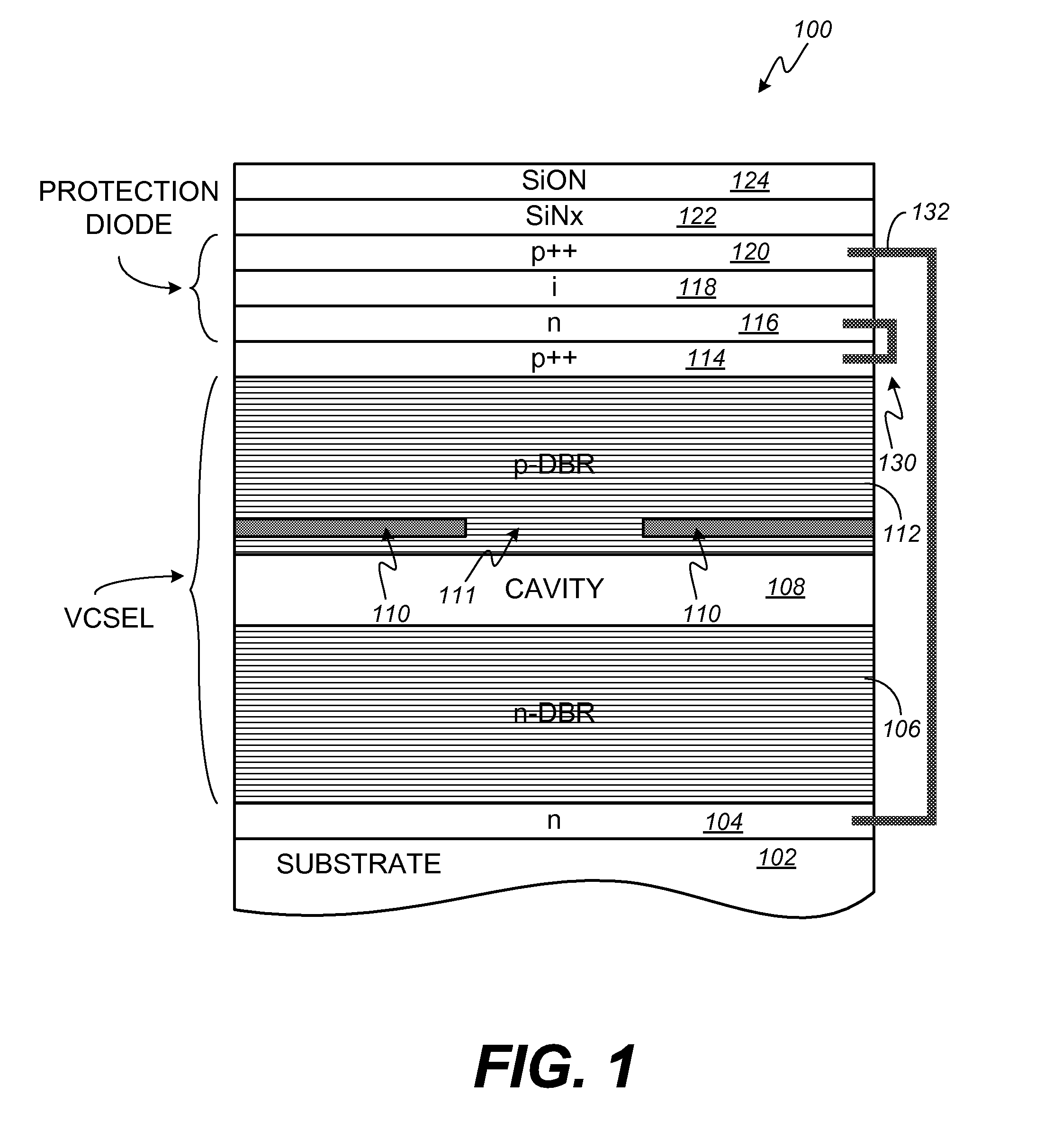
Vertical cavity surface emitting lasers (VCSELs) are widely used as light sources for optical interconnect devices, storage area networks, and sensors. In order to enable VCSELs to operate at increasingly higher speeds, or data rates, the aperture sizes must be made increasingly smaller. Decreasing the size of the aperture, however, makes the VCSEL increasingly susceptible to electrostatic discharge (ESD) damage. Failure from an ESD event is a frequent cause of customer returns of VCSELs. VCSELs have a p-intrinsic-n (PIN) structure and the damage threshold for ESD is asymmetric, i.e., an ESD pulse traveling in the reverse-bias direction is more damaging than an ESD pulse traveling in the forward-bias direction. The ESD damage threshold for VCSELs is commonly characterized by models such as the human body model (HBM) and the machine model (MM). For a VCSEL aperture diameter in the range of 5-10 micrometers (microns), the HBM damage threshold voltage is typically in the range of 100 to 200 volts (V) and the MM damage threshold voltage is typically under 50 V. It is known to integrate a protection diode with a laser diode in a semiconductor device. For example, U.S. Pat. Nos. 6,185,240, 7,508,047 and 7,693,201 each disclose semiconductor devices in which a laser diode and a protection diode are integrated together in a semiconductor material. One of the problems associated with integrating the protection diode together with the laser diode in the same semiconductor is that the inclusion of the protection diode introduces capacitance, which limits the operating speed of the laser diode. The capacitance Cdof the protection diode can be expressed as: where, ε is the permittivity of the semiconductor material, A is the area of protection diode, and D is the width of depletion region of the protection diode. Decreasing the area, A, or increasing the width, D, of the depletion region will decrease the capacitance, Cd, of the protection diode. Decreasing area A to reduce Cdis not desirable because a small area A leads to a high thermal resistance and high current density. The high thermal resistance will lead to rapid temperature rise during an ESD event and result in a low damage threshold. On the other hand, increasing the area, A, of the protection diode increases the damage threshold voltage of the laser diode, but also increases the amount of capacitance that is introduced by the protection diode, which limits the operating speed, or the data rate that can be supported by the laser diode. For example, U.S. Pat. No. 7,508,047 shows a Zener diode that is placed below the VCSEL. In the illustrated embodiment, the area of the Zener diode is larger than the area of the VCSEL aperture and the depletion layer of the p+/n+ junction is relatively thin. These two factors result in a large capacitance that protects the VCSEL but renders the combination device unsuitable for signal operation above about 1 Gb/s. The most common configuration of a VCSEL is a conducting n-type substrate with an n-type distributed Bragg reflector (DBR), an active region (intrinsic layer), and a p-type DBR sequentially grown on it. Although the design described in U.S. Pat. No. 6,185,240 can be configured such that Cdis relatively small; the design cannot be used in the common VCSEL configuration described above because the cathode (n-side) of the VCSEL and diode are always connected through the substrate. Consequently, the substrate cannot be a conducting substrate. An improved VCSEL with an integrated protection diode (IPD) consistent with the present invention is a two-terminal semiconductor device. The VCSEL with an IPD uses a p-i-n arrangement of semiconductor materials to enable the protective diode between the aperture of the VCSEL and the emitting surface. The damage threshold for electro-static discharge events with the human body model are increased from 100-200 V to nearly 1 kV. The p-i-n arrangement minimizes diode capacitance to enable operation of the VCSEL at data rates in excess of 10 Gb/s. The VCSEL portion of the improved VCSEL with an IPD can be fabricated on both conducting n-type or p-type substrates and semi-insulating substrates. In addition, the VCSEL portion of the improved VCSEL with an IPD can be modulated with an anode drive signal (i.e., coupling a data signal on the p-side of the device), a cathode drive signal (i.e., coupling a data signal on the n-side of the device) or differentially. By arranging the protection diode above (or adjacent) to the VCSEL, the resulting device reduces the area required to produce a suitably protected VCSEL capable of producing an optical signal at high data rates. An embodiment of the present invention relates to a two-terminal semiconductor device including a substrate, a first layer of a semiconductor material, a VCSEL, a second layer of a semiconductor material and a protection diode. The substrate has the first layer of a semiconductor material disposed on an upper surface. The VCSEL is disposed on an upper surface of the first layer of semiconductor material. The VCSEL is formed by a stacked pair of distributed Bragg reflectors arranged both below and above an active region. The VCSEL is further configured with an oxide layer that defines an aperture within the device. The second layer of a semiconductor material is arranged between the VCSEL and the protection diode. The protection diode is implemented using a set of stacked layers in a p-i-n arrangement. An ohmic p-type contact pad and an ohmic n-type contact pad are arranged in contact with both the VCSEL and the protection diode to form the terminals of the semiconductor device. In an exemplary embodiment, a method for providing electrostatic discharge protection in a semiconductor device is disclosed. The method includes the steps of providing a substrate with an upper surface, forming at least one layer of semiconductor material on the upper surface of the substrate, forming a vertical cavity surface emitting laser disposed on the at least one layer of semiconductor material, the vertical cavity surface emitting laser having a first distributed Bragg reflector formed in a first set of layers, an intrinsic layer containing a light-emitting material disposed on top of the first plurality of layers, a second distributed Bragg reflector formed in a second set of layers, the vertical cavity surface emitting laser having an oxide layer proximal to the intrinsic layer arranged in the second set of layers, the oxide layer defining an aperture, forming a second layer of semiconductor material disposed on the second set of layers, forming a protection diode that in operation protects the vertical cavity surface emitting laser from electrostatic discharge events, the protection diode disposed on the second layer of semiconductor material located above the aperture, the protection diode having an intrinsic layer above a n-type layer and below a p++ type semiconductor material, forming an ohmic p-type contact pad in contact with the vertical cavity surface emitting laser and the protection diode, and forming an ohmic n-type contact pad in contact with the vertical cavity surface emitting laser and protection diode. Other systems, methods, features, and advantages will be or become apparent to one with skill in the art upon examination of the following figures and detailed description. It is intended that all such additional systems, methods, features, and advantages be included within this description, be within the scope of the specification, and be protected by the accompanying claims. An improved VCSEL with an integrated protective diode and methods for manufacturing the same can be better understood with reference to the following drawings. The components in the drawings are not necessarily to scale, emphasis instead being placed upon clearly illustrating the principles of the present invention. The described issues with integrating a protection diode with a laser diode in a semiconductor device, while still being able to support data rates above 10 Gb/s, as exemplified in the state of the art, are addressed by integrating a protection diode between a VCSEL and an emitting surface of a semiconductor device. By arranging a reverse-biased protection diode in a region above an aperture of the VCSEL, the improved semiconductor device minimizes the area required to implement the protection diode. As will be explained below, the size of the protection diode and the thickness of the intrinsic layer therein can be modified to achieve a desired capacitance to strike a balance between protection from ESD events and the capability to support data rates in excess of about 10 Gb/s. The VCSEL can be fabricated on both conducting (n-type or p-type) substrates and semi-insulating substrates. It will be understood that the polarity of the protection diode will change with a change in polarity of the VCSEL. It will be further understood that the protection diode need not be precisely coaxial with the aperture. That is, the protection diode can be offset from the axis of the aperture of the VCSEL. Illustrative, or exemplary, embodiments will now be described with reference to A p++ layer 114 is disposed above the second or upper p-DBR 112. A protection diode is disposed on the p++ layer 114. A layer 116 of n-type material is disposed above the p++ layer 114. An intrinsic region or i-layer 118 is disposed above layer 116. A p++ layer 120 is disposed above the i-layer 118. As indicated in Dielectric layers 122 and 124 are passivation layers deposited during device fabrication. In the illustrated embodiment the second dielectric layer 124 is made from SiON. Connection 130 conductively and physically couples p++ layer 114 to n-type layer 116. Similarly, connection 132 conductively and physically couples p++ layer 120 to n-type layer 104. The protection diode provides a low impedance path for ESD pulses traveling in the reverse-bias direction of the VCSEL, while ESD pulses traveling in the forward-bias direction of the VCSEL pass mainly through the VCSEL. Thus, the protection diode protects the VCSEL from ESD events that can cause the greatest damage to the VCSEL, namely, ESD pulses traveling in the reverse-bias direction. As further shown in The n-contact 318 is deposited on the exposed portion of layer 116 such that it overlaps and electrically contacts p-contact 314. In this way, the p-contact 314 and n-contact 318 electrically couple the n-type layer 116 of the protection diode 220 with the p++ layer 114 of the VCSEL 210. A first dielectric layer 122, which may be made from silicon nitride (SiN) is applied or otherwise provided above the p++ layer 120. A second dielectric layer 124 which may be silicon oxynitride (SiON) is disposed over exposed regions of the semiconductor to serve as a passivation layer. A portion of the layers 122 and 124, in registration above a portion of mesa 320 and p++ layer 120 of protection diode 220 is removed and replaced by p-contact 322, which may be a bilayer film of Ti/Au. As further indicated in The p-contact 314, the n-contact 318, mesa 320, and p-contact 322 are shown in Accordingly, it will be appreciated that the area of the protection diode can be precisely controlled by placement of the mesa 320. Moreover, it should be appreciated that the thickness of the intrinsic layer 118 of the protection diode 220 can be precisely controlled by monitoring epitaxial growth of the intrinsic layer 118 above the n-type layer 116. Accordingly, the capacitance introduced by the protection diode 220 can be controllably adjusted to enable the VCSEL 210 to operate at data rates in excess of about 10 Gb/s, while in turn providing sufficient protection against potentially catastrophic electro-static discharge events in the reverse-bias direction. The p++ layer 120, intrinsic layer 118 and the n-type layer 116 of the protection diode 220 may modify the reflectance of the upper p-type DBR 112 of the VCSEL 210, and are taken into account in the VCSEL design. For example, the thicknesses of each of these layers may be made equal to a suitable multiple of the half-wavelength of the light emitted during operation of the VCSEL. For operation of the VCSEL 210 at high data rates, the parasitic capacitance arising from the additional semiconductor junction between n-type layer 116 and the p++ layer 120 of the protection diode 220, as well as the parasitic capacitance arising from the interconnect 312 and an interconnect coupled to p-contact 314 (not shown), should be kept small. The internal metal connection provided by the diode n-contact 318 to VCSEL p-contact 314 contributes negligible capacitance and inductance. Interconnect 312, which couples the p++ layer 120 of the protection diode 220 to the n-contact of the VCSEL 210 is applied over the thick dielectric layer 124 and/or dielectric layer 122. Consequently, the interconnect 312 can be several microns wide and still contribute only a small amount of capacitance and inductance. The invention is not limited with respect to the chemical elements or compounds that are used for the various layers of the semiconductor device 100 or the semiconductor device 300. Known semiconductor processes may be used to fabricate the example semiconductor devices, and a variety of materials may be used to make the same. An example of materials that may be used to make the semiconductor device 100 or the semiconductor device 300 is as follows: the substrate 102 is made of n-doped gallium arsenide (GaAs); the layer 104 is made up of n-doped GaAs; the lower or n-DBR 106 is made up of several layers of n-doped aluminum gallium arsenide (AlGaAs) having different percentages of Al or Ga to make them alternate between high and low refractive indices; the cavity 108 contains GaAs quantum wells that are un-doped or have a very low doping; the upper or p-DBR 112 is made up of several layers of p-doped AlGaAs having different percentages of Al or Ga to make them alternate between high and low refractive indices; the p++ layer 114 is made up of highly p-doped AlGaAs; n-type layer 116 is made from n-doped AlGaAs; the intrinsic layer 118 of the protection diode is made up of AlGaAs that is un-doped or that has a very low doping; the layer 120 is made up of highly p-doped GaAs; layer 122 is made of a dielectric material such as silicon nitride (SiN); and the layer 124 is made of a dielectric material such as silicon oxynitride (SiON). While the described semiconductor devices are made primarily of GaAs related materials, other compounds may be used for the semiconductor device 100 or the semiconductor device 300. The compounds can be selected to have desired bandgap energies that enable desired light emission wavelengths to be produced. Examples of other suitable materials that may be used include, but are not limited to, aluminum gallium arsenide (AlGaAs), gallium phosphide (GaP), indium gallium phosphide (InGaP), gallium nitride (GaN), indium gallium arsenide (InGaAs), indium gallium arsenide nitride (InGaNAs), indium phosphide (InP), and gallium indium phosphide (GaInP). It should also be noted that layers that are designated in It should also be noted that the invention is not limited with respect to the manner in which the VCSEL modulation signal is applied to the VCSEL 210. For example, the modulation signal may be applied to the VCSEL 210 on the p side (i.e., anode drive), on the n side (i.e., cathode drive by replacing the n-type substrate with a semi-insulating substrate), or differentially (i.e., a differential signal applied across the p and n sides of the VCSEL 210. It should be noted that the invention has been described with reference to illustrative embodiments and that the invention is not limited to these specific embodiments. Those skilled in the art will understand the manner in which modifications can be made to the illustrative embodiments and that all such modifications are within the scope of the invention. For example, while A semiconductor device includes a vertical cavity surface emitting laser (VCSEL) with an integrated protection diode arranged between the VCSEL and an emitting surface. By locating the protection diode above the VCSEL, a minimal increase in substrate area is consumed to protect the VCSEL from electrostatic discharge events. A relatively small capacitance introduced by the protection diode, is controllably adjusted by one of the radial size of the protection diode and the thickness of the intrinsic layer therein. The relatively small capacitance introduced by the protection diode enables the VCSEL to operate at data rates above 10 Gb/s. 1. A semiconductor device comprising:
a substrate having at least one layer of semiconductor material formed on an upper surface thereof; a vertical cavity surface emitting laser disposed on the upper surface of the at least one layer of semiconductor material, the vertical cavity surface emitting laser having a first distributed Bragg reflector formed in a first set of layers, wherein at least one of the first set of layers is of an n-type material, a cavity containing a light-emitting material disposed on top of the first plurality of layers, a second distributed Bragg reflector formed in a second set of layers, and a first p++ layer disposed on the second set of layers, wherein at least one of the second set of layers is of a p-type material, the vertical cavity surface emitting laser having an oxide layer proximal to the intrinsic layer arranged in the second set of layers, the oxide layer defining an aperture; a protection diode for protecting the vertical cavity surface emitting laser from electrostatic discharge events disposed on the first p++ layer located above the aperture, the protection diode having at least one layer of n-type semiconductor material disposed on the first p++ layer, an intrinsic layer disposed on the at least one layer of n-type semiconductor material, and a second p++ layer disposed on the intrinsic layer; an ohmic p-type contact pad and an ohmic n-type contact pad in contact with the vertical cavity surface emitting laser and protection diode; a first metal interconnect connecting the p-contact pad of the vertical cavity surface emitting laser with the n-contact of the protection diode; and a second metal interconnect connecting the n-contact pad of the vertical cavity surface emitting laser with the p-contact of the protection diode. 2. The semiconductor device of 3. The semiconductor device of 4. The semiconductor device of 5. The semiconductor device of 6. The semiconductor device of 7. The semiconductor device of 8. The semiconductor device of 9. The semiconductor device of at least one layer of dielectric material disposed on the semiconductor device and electrically isolating the p-contact pad and n-contact pad from each other, wherein the intrinsic layer reduces a capacitance of the protection diode to allow the vertical cavity surface emitting laser to operate at data rates above 10 Gb/s. 10. A semiconductor device comprising:
a substrate having at least one layer of semiconductor material formed on an upper surface thereof; a vertical cavity surface emitting laser disposed on the upper surface of the at least one layer of semiconductor material, the vertical cavity surface emitting laser having a first distributed Bragg reflector formed in a first set of layers, wherein at least one of the first set of layers is of a p-type material, a cavity containing a light-emitting material disposed on top of the first plurality of layers, a second distributed Bragg reflector formed in a second set of layers, and a first n++ layer disposed on the second set of layers, wherein at least one of the second set of layers is of a n-type material, the vertical cavity surface emitting laser having an oxide layer proximal to the intrinsic layer arranged in the second set of layers the oxide layer defining an aperture; a protection diode for protecting the vertical cavity surface emitting laser from electrostatic discharge events disposed on the first n++ layer located above the aperture, the protection diode having at least one layer of p++ type semiconductor material disposed on the first n++ layer, an intrinsic layer disposed on the at least one layer of p++ type semiconductor material, and a second n++ layer disposed on the second intrinsic layer; an ohmic p-type contact pad and an ohmic n-type contact pad in contact with the vertical cavity surface emitting laser and protection diode; a first metal interconnect connecting the n-contact pad of the vertical cavity surface emitting laser with the p-contact of the protection diode; and a second metal interconnect connecting the p-contact pad of the vertical cavity surface emitting laser with the n-contact of the protection diode. 11. The semiconductor device of 12. The semiconductor device of 13. The semiconductor device of 14. The semiconductor device of 15. The semiconductor device of 16. The semiconductor device of at least one layer of dielectric material disposed on the semiconductor device and electrically isolating the p-contact pad and n-contact pad from each other, wherein the intrinsic layer reduces a capacitance of the protection diode to allow the vertical cavity surface emitting laser to operate at data rates above 10 Gb/s. 17. A method for providing electrostatic discharge protection in a semiconductor device, the method comprising:
providing a substrate with an upper surface; forming at least one layer of semiconductor material on the upper surface of the substrate; forming a vertical cavity surface emitting laser disposed on the at least one layer of semiconductor material, the vertical cavity surface emitting laser having a first distributed Bragg reflector formed in a first set of layers, an intrinsic layer containing a light-emitting material disposed on top of the first plurality of layers, a second distributed Bragg reflector formed in a second set of layers, the vertical cavity surface emitting laser having an oxide layer proximal to the intrinsic layer arranged in the second set of layers, the oxide layer defining an aperture; forming a second layer of semiconductor material disposed on the second set of layers; and forming a protection diode that in operation protects the vertical cavity surface emitting laser from electrostatic discharge events, the protection diode disposed on the second layer of semiconductor material located above the aperture, the protection diode having an intrinsic layer above a n-type layer and below a p++ type semiconductor material; forming an ohmic p-type contact pad in contact with the vertical cavity surface emitting laser and the protection diode; and forming an ohmic n-type contact pad in contact with the vertical cavity surface emitting laser and protection diode. 18. The method of 19. The method of 20. The method of BACKGROUND
SUMMARY
BRIEF DESCRIPTION OF THE DRAWINGS
DETAILED DESCRIPTION