Organic Light-Emitting Diode Display With Enhanced Aperture Ratio
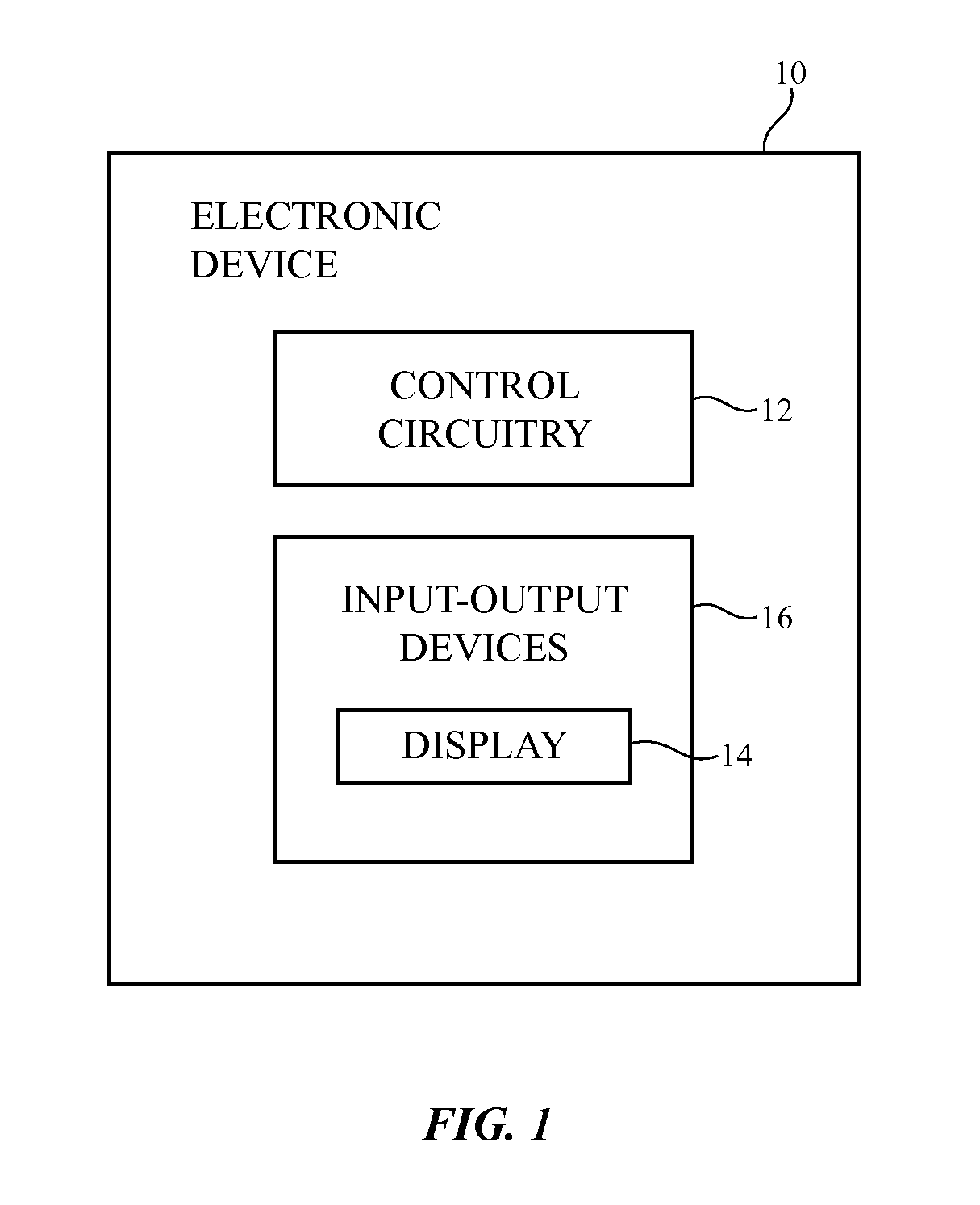
This relates generally to displays, and, more particularly, to organic light-emitting diode displays. Electronic devices often include displays. Organic light-emitting diode displays may exhibit desirable attributes such as a wide field of view, compact size, and low power consumption. Organic light-emitting diode displays have arrays of pixels. Each pixel may contain an organic light-emitting diode and thin-film transistor circuitry that that controls current flow through the organic light-emitting diode. Storage capacitors may be used to store data between successive image frames. It can be challenging to form an organic light-emitting diode display. If care is not taken, the structures that form the thin-film transistor circuitry for controlling the pixels may consume more area than desired, thereby restricting the amount of light-emitting area per pixel (i.e., limiting the aperture ratio of the pixels). It may also be difficult to form storage capacitors without consuming more area within a pixel than desired. It would therefore be desirable to be able to form an organic light-emitting diode display with enhanced aperture ratios and storage capacitor structures. An organic light-emitting diode display may have an array of pixels. Each pixel may have an organic light-emitting diode with an anode and cathode. The anodes may be formed from a patterned layer of metal. Thin-film transistor circuitry in the pixels may include transistors such as drive transistors and switching transistors. Data lines may supply data signals to the pixels and horizontal control lines may supply control signals to the gates of the transistors. Voltage initialization lines may be used to distribute voltages to columns of the pixels for use during threshold voltage compensation operations. A switching transistor may be coupled between a voltage initialization line and each anode. The voltage initialization lines and capacitor structures in the thin-film transistor circuitry may be formed using a layer of metal that is different than the layer of metal that forms the anodes. An illustrative electronic device of the type that may be provided with an organic light-emitting diode display is shown in Input-output circuitry in device 10 such as input-output devices 12 may be used to allow data to be supplied to device 10 and to allow data to be provided from device 10 to external devices. Input-output devices 12 may include buttons, joysticks, scrolling wheels, touch pads, key pads, keyboards, microphones, speakers, tone generators, vibrators, cameras, sensors, light-emitting diodes and other status indicators, data ports, etc. A user can control the operation of device 10 by supplying commands through input-output devices 12 and may receive status information and other output from device 10 using the output resources of input-output devices 12. Input-output devices 12 may include one or more displays such as display 14. Display 14 may be a touch screen display that includes a touch sensor for gathering touch input from a user or display 14 may be insensitive to touch. A touch sensor for display 14 may be based on an array of capacitive touch sensor electrodes, acoustic touch sensor structures, resistive touch components, force-based touch sensor structures, a light-based touch sensor, or other suitable touch sensor arrangements. Control circuitry 16 may be used to run software on device 10 such as operating system code and applications. During operation of device 10, the software running on control circuitry 16 may display images on display 14. Display 14 may be an organic light-emitting diode display. Display driver circuitry may be used to control the operation of pixels 22. The display driver circuitry may be formed from integrated circuits, thin-film transistor circuits, or other suitable circuitry. Display driver circuitry 28 of To display the images on display pixels 22, display driver circuitry 28 may supply image data to data lines D while issuing clock signals and other control signals to supporting display driver circuitry such as gate driver circuitry 18 over path 50. If desired, circuitry 28 may also supply clock signals and other control signals to gate driver circuitry on an opposing edge of display 14. Gate driver circuitry 18 (sometimes referred to as horizontal control line control circuitry) may be implemented as part of an integrated circuit and/or may be implemented using thin-film transistor circuitry. Horizontal control lines G in display 14 may gate line signals (scan line signals), emission enable control signals, and other horizontal control signals for controlling the pixels of each row. There may be any suitable number of horizontal control signals per row of pixels 22 (e.g., one or more, two or more, three or more, four or more, etc.). Each column of pixels 22 preferably includes a sufficient number of data lines to supply image data for all of the subpixels of that column (e.g., a red data line for carrying red data signals to red subpixels, a green data line for carrying green data signals to green subpixels, and a blue data line for carrying blue data signals to blue subpixels). The circuitry for each subpixel may include an organic light-emitting diode, a drive transistor that controls current flow through the diode, and supporting transistors (e.g., switching transistors and emission enable control transistors). The supporting transistors may be used in performing data loading operations and threshold voltage compensation operations for the drive transistors. Each subpixel may have one or more capacitors. Storage capacitors may be used to store data signals between successive frames of data. A schematic diagram of an illustrative circuit for an organic light-emitting diode subpixel (pixel) is shown in In each subpixel 22SUB, the state of drive transistor TD controls the amount of drive current IDflowing through diode 38 and therefore the amount of emitted light 40 from subpixel 22SUB. Each diode 38 has an anode A and a cathode CD. Drive current IDflows between anode A and cathode CD. Cathode CD of diode 38 is coupled to ground terminal 36, so cathode terminal CD of diode 38 may sometimes be referred to as the ground terminal for diode 38. Cathode CD may be shared among multiple diodes (i.e., the cathodes CD of multiple diodes may be tied to a shared voltage). Each anode A is individually driven by a respective drive transistor TD. To ensure that transistor 38 is held in a desired state between successive frames of data, subpixel 22SUB may include a storage capacitor such as storage capacitor Cst1. The voltage on storage capacitor Cst1 is applied to the gate of transistor TD at node ND2 to control transistor TD (i.e., to control the magnitude of drive current ID). Data can be loaded into storage capacitor Cst1 using one or more switching transistors. One or more emission enable transistors may be used in controlling the flow of current through drive transistor TD. In the example of Display driver circuitry 28 may supply initialization voltages to columns of pixels using vertical initialization voltages lines in each column. As shown in Using pixel circuitry of the type shown in During the initialization phase, circuitry 18 may assert SCAN1 and SCAN2 (i.e., SCANT and SCAN2 may be taken high). This turns on transistors TS1 and TS2 so that reference voltage signal Vref from line D and initialization voltage signal Vini from the initialization voltage line are applied to nodes ND2 and ND3, respectively. During the threshold voltage generation phase of the compensation period, signal EM is asserted so that transistor TE is turned on and current IDflows through drive transistor TD to charge up the capacitance at node ND3. As the voltage at node ND3 increases, the current through drive transistor TD will be reduced because the gate-source voltage Vgs of drive transistor TD will approach the threshold voltage Vt of drive transistor TD. The voltage at node ND3 will therefore go to Vref-Vt. After compensation (i.e., after initialization and threshold voltage generation), data is programmed into the compensated display pixels. During programming, emission transistor TE is turned off by deasserting signal EM and a desired data voltage D is applied to node ND2 using data line D. The voltage at node ND2 after programming is display data voltage Vdata. The voltage at node ND3 rises because of coupling with node ND2. In particular, the voltage at node ND3 is taken to Vref−Vt+(Vdata−Vref)*K, where K is equal to Cst1/(Cst1+Cst2+Coled), where Coled is the capacitance associated with diode 38. After compensation and programming operations have been completed, the display driver circuitry of display 14 places the compensated and programmed pixels into the emission mode (i.e., the emission period is commenced). During emission, signal EM is asserted for each compensated and programmed subpixel to turn on transistor TE. The voltage at node ND3 goes to Voled, the voltage associated with diode 38. The voltage at node ND2 goes to Vdata+(Voled−(Vref−Vt)−(Vdata−Vref)*K. The value of Vgs-Vt for drive transistor TD is equal to the difference between the voltage Va of node ND2 and the voltage Vb of node ND3. The value of Va−Vb is (Vdata−Vref)*(1−K), which is independent of Vt. Accordingly, each subpixel 22SUB in the array of pixels in display 14 has been compensated for threshold voltage variations so that the amount of light 40 that is emitted by each subpixel 22SUB is proportional only to the magnitude of the data signal D for each of those subpixels. The illustrative pixel circuit of Organic light-emitting diode pixels such as subpixel 22SUB of Dielectric layer 46 may have an opening that serves to define the layout of the light-emitting diode for each subpixel (e.g., alignment of the emissive material 47 with respect to anode 44) and may sometimes be referred to as a pixel definition layer. Planarization layer 50 (e.g., an organic polymer layer) may be formed on top of thin-film transistor structures 52. Thin-film transistor structures 52 may be formed on substrate 24. Substrate 24 may be rigid or flexible and may be formed from glass, ceramic, crystalline material such as sapphire, polymer (e.g., a flexible layer of polyimide or a flexible sheet of other polymer material), etc. Thin-film transistor structures 52 may include silicon transistors such as silicon transistors or thin-film transistors formed from other semiconductors (e.g., semiconducting oxides such as indium gallium zinc oxide). In the illustrative configuration of The channel regions formed from semiconductor layer 62 may be covered by gate insulator layer 64 (e.g., a layer of silicon oxide or other inorganic layer). Transistor gates 66 may be formed from a gate layer such as a layer of patterned metal (e.g., molybdenum, as an example). Gates 66 may be covered by a layer of interlayer dielectric (e.g., silicon oxide layer 68, silicon nitride layer 70, and/or other oxide and nitride layers or other organic or inorganic layers). Source-drain layer 74 may be a layer of metal that is patterned to form transistor source-drain terminals for transistors in circuitry 72 such as transistors 200 and TD. Each transistor may have a pair of source-drain terminals connected to opposing sides of the channel 62 of that transistor. Circuitry 72 may also include capacitor structures such as capacitors Cst1 and Cst2 of An inorganic passivation layer such as passivation layer 106 may be interposed between polymer (organic) passivation layer 50 and source-drain layer 74 (and dielectric layer 70). Layer 106 may be formed from silicon nitride or other dielectric. Buffer layer 122 may be formed on substrate 24. Buffer layer 122 may be formed from one or more layers of inorganic dielectric material or other dielectric. As an example, buffer layer 122 may include lower buffer layer 122-1 on substrate 24 and upper buffer layer 122-2 on layer 122-1. Layers 122-1 and 122-2 may be formed from silicon oxide, silicon nitride, oxynitride, or other dielectric materials. Layer 122 may help to block impurities from substrate 24 (e.g., glass impurities) and thereby prevent these impurities from degrading the performance of the thin-film transistors of thin-film transistor circuitry 52. Back-side metal layer 118 may be formed under the thin-film transistors (e.g., transistors 200 and TD in the example of To help enhance the aperture ratio of the pixels of display 14, anode layer 44 can be used exclusively or nearly exclusively for forming anodes A. With this type of approach, additional signal paths for display 14 such as the Vini lines in display 14 can be formed using portions of other metal layers and need not be formed from the metal of the anode layer. In the example of The conductive layers of In the illustrative configuration of As shown in The structures of In the illustrative configuration of The structures of In the illustrative configuration of The structures of In the illustrative configuration of Layer 218 may be used in forming capacitors for circuitry 72 such as capacitors Cst1 and Cst2. For example, layer 218 may form a capacitor electrode and metal from gate metal layer 66 may form a capacitor electrode. The electrodes formed from layers 218 and 66 may be separated by interposed dielectric layer 68. Capacitors may also be formed using portions of layer 218 and portions of source-drain layer 74 as electrodes that are separated by interposed dielectric layer 70. In the illustrative configuration of If desired, portions of source-drain layer 74 such as portion 74′ may be used in forming capacitors for circuitry 72 such as capacitors Cst1 and Cst2. For example, layer 74′ may form a capacitor electrode and metal from gate metal layer 66 may form a capacitor electrode. The electrodes formed from layers 74′ and layer 66 may be separated by interposed interlayer dielectric layers 68 and 70. In the illustrative configuration of The foregoing is merely illustrative and various modifications can be made by those skilled in the art without departing from the scope and spirit of the described embodiments. The foregoing embodiments may be implemented individually or in any combination. An organic light-emitting diode display may have an array of pixels. Each pixel may have an organic light-emitting diode with an anode and cathode. The anodes may be formed from a patterned layer of metal. Thin-film transistor circuitry in the pixels may include transistors such as drive transistors and switching transistors. Data lines may supply data signals to the pixels and horizontal control lines may supply control signals to the gates of the transistors. A switching transistor may be coupled between a voltage initialization line and each anode. The voltage initialization lines and capacitor structures in the thin-film transistor circuitry may be formed using a layer of metal that is different than the layer of metal that forms the anodes. 1. A display, comprising:
an array of pixels each of which has an organic light-emitting diode having an anode and a cathode and each of which has thin-film transistor circuitry with transistors that include at least one drive transistor and at least one switching transistor; horizontal control lines that are coupled to gates in the transistors and that supply control signals to rows of the pixels in the array; data lines associated with columns of the pixels in the array; and initialization voltage lines associated with columns of the pixels in the array, wherein in each pixel the switching transistor couples one of the voltage initialization lines to the anode of the organic light-emitting diode in that pixel, wherein the thin-film transistor circuitry includes a semiconductor layer that forms semiconductor channels for the transistors, a gate insulator layer adjacent to the semiconductor layer, a gate layer that is adjacent to the gate insulator layer and that is patterned to form the gates, a source-drain layer that is patterned to form source-drain terminals for the transistors, a dielectric layer on the source-drain layer, a metal anode layer that is patterned to form the anodes in the pixels, an organic passivation layer that is interposed between the dielectric layer and the metal anode layer, and an additional metal layer that is not formed from a portion of the metal anode layer and that is patterned to form the voltage initialization lines. 2. The display defined in 3. The display defined in 4. The display defined in 5. The display defined in 6. The display defined in 7. The display defined in 8. The display defined in 9. The display defined in 10. The display defined in 11. The display defined in 12. The display defined in 13. The display defined in 14. The display defined in 15. The display defined in 16. The display defined in 17. The display defined in 18. The display defined in a metal shield layer under the transistors; a first dielectric buffer layer, wherein the first dielectric buffer layer is interposed between the metal shield layer and the semiconductor layer; and a second dielectric buffer layer, wherein the second dielectric buffer layer is interposed between the additional metal layer and the metal shield layer. 19. The display defined in a metal shield layer under the transistors; a first dielectric buffer layer, wherein the first dielectric buffer layer is interposed between the metal shield layer and the semiconductor layer; and a second dielectric buffer layer, wherein the metal shield layer is interposed between the first and second dielectric buffer layers and wherein the additional metal layer is a interposed between the first dielectric buffer layer and the gate insulator layer. 20. The display defined in an interlayer dielectric layer between the source-drain layer and the gate layer, wherein the additional metal layer is interposed between the interlayer dielectric layer and the gate insulator layer and is formed from a portion of the gate layer. 21. The display defined in 22. A display, comprising:
an array of pixels each of which has an organic light-emitting diode having an anode and a cathode and each of which has thin-film transistor circuitry with transistors including at least one drive transistor and at least one switching transistor; horizontal control lines that are coupled to gates in the transistors and that supply control signals to rows of the pixels in the array; data lines associated with columns of the pixels in the array; and initialization voltage lines associated with columns of the pixels in the array, wherein in each pixel the switching transistor couples one of the voltage initialization lines to the anode of the organic light-emitting diode in that pixel, wherein the thin-film transistor circuitry includes a semiconductor layer that forms semiconductor channels for the transistors, a gate insulator layer adjacent to the semiconductor layer, a gate layer that is adjacent to the gate insulator layer and that is patterned to form the gates, a source-drain layer that is patterned to form source-drain terminals for the transistors, a dielectric layer on the source-drain layer, a metal anode layer that is patterned to form the anodes in the pixels, an organic passivation layer that is interposed between the dielectric layer and the metal anode layer, and an additional metal layer that is not formed from a portion of the metal anode layer and that is patterned to form the voltage initialization lines and wherein the additional metal layer has a portion that forms a shield layer under the transistors that is separate from the initialization voltage lines. 23. A display, comprising:
an array of pixels each of which has an organic light-emitting diode having an anode and a cathode and each of which has thin-film transistor circuitry with transistors including at least one drive transistor and at least one switching transistor; horizontal control lines that are coupled to gates in the transistors and that supply control signals to rows of the pixels in the array; data lines associated with columns of the pixels in the array; and initialization voltage lines associated with columns of the pixels in the array, wherein in each pixel the switching transistor couples one of the voltage initialization lines to the anode of the organic light-emitting diode in that pixel, wherein the thin-film transistor circuitry includes a semiconductor layer that forms semiconductor channels for the transistors, a gate insulator layer adjacent to the semiconductor layer, a gate layer that is adjacent to the gate insulator layer and that is patterned to form the gates, a source-drain layer that is patterned to form source-drain terminals for the transistors, a dielectric layer on the source-drain layer, a metal anode layer that is patterned to form the anodes in the pixels, an organic passivation layer that is interposed between the dielectric layer and the metal anode layer, and an additional metal layer that is not formed from a portion of the metal anode layer and that is patterned to form the voltage initialization lines, wherein the additional metal layer is interposed between the gate layer and the source-drain layer, and wherein the additional metal layer is interposed between first and second inorganic dielectric layers.BACKGROUND
SUMMARY
BRIEF DESCRIPTION OF THE DRAWINGS
DETAILED DESCRIPTION