ELECTROCHROMIC DEVICE AND METHOD OF DRIVING THE SAME, LENS UNIT, IMAGE PICKUP APPARATUS, AND WINDOW MEMBER
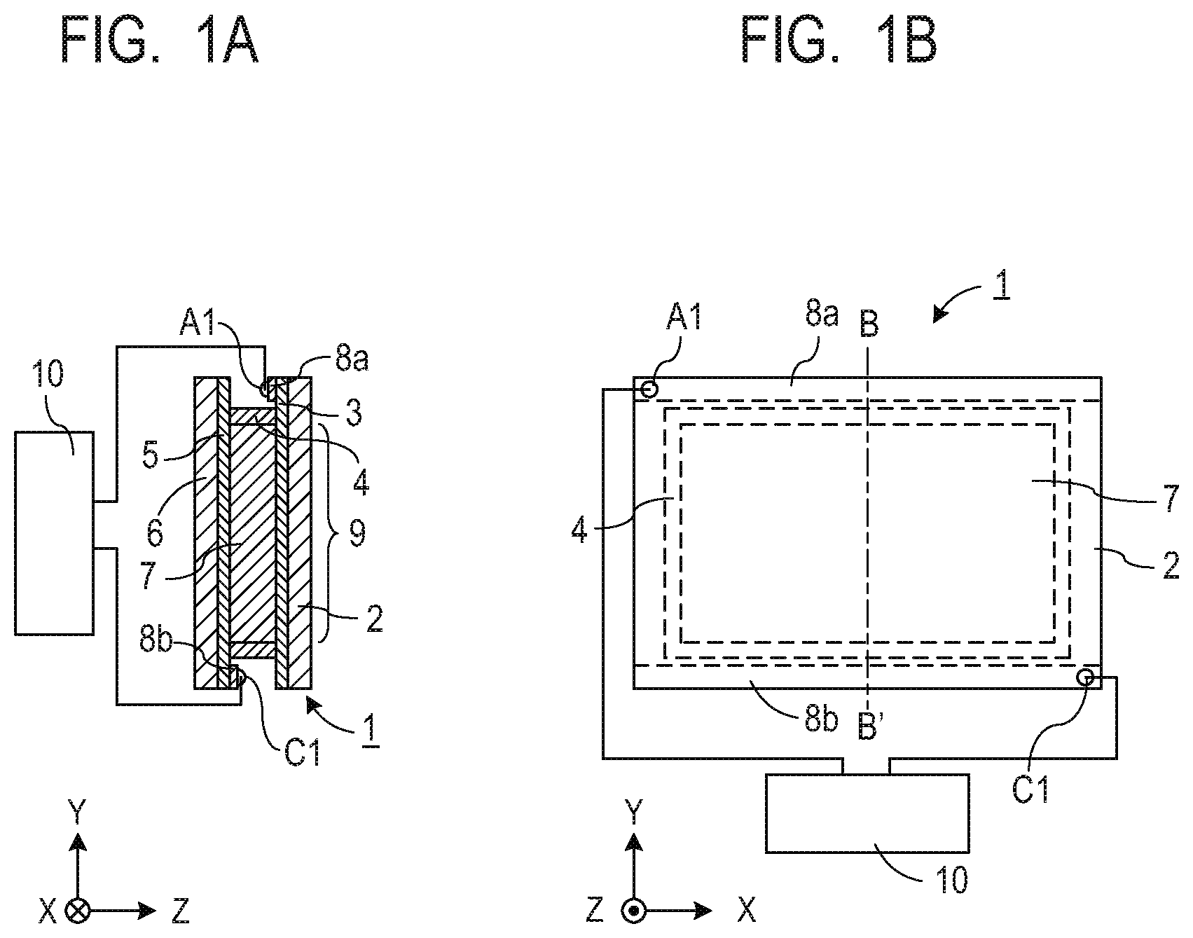
The present disclosure generally relates to an electrochromic device using an electrochromic element and a method of driving the electrochromic device. The present disclosure also relates to a lens unit, an image pickup apparatus, and a window member each of which includes the electrochromic device. A compound that is changed in optical characteristics such as absorption wavelength and absorbance for a substance by an electrochemical redox reaction is called “electrochromic (EC) compound”. An EC element utilizing the EC compound is applied, for example, to a display device, a variable reflectance mirror, and a variable transmission window. EC elements formed of organic EC compounds include a “complementary” EC element including, as an EC layer, an EC solution containing an anodic organic EC material, which is colored by oxidation, and a cathodic organic EC material, which is colored by reduction. Such a complementary EC element is decolored by an electrode reaction, in which a wire between electrodes is short-circuited to rereduce cations and reoxidize anions, and by a self-decoloring reaction, in which cations and anions associate with each other are caused to disappear. In general, decoloration of the organic EC element is rate-determined by diffusion of the material, and hence decoloring response becomes faster as the element has a smaller gap between the electrodes and a shorter diffusion length. Meanwhile, as the environment has a lower temperature, there is a problem in that the diffusion of the material becomes slower so that the decoloring response becomes slower, resulting in being required to consider an acceleration drive method. In Japanese Patent Application Laid-Open No. 2014-098934 (hereinafter PTL 1), it is described, as a method of decoloring an organic EC element, to apply a voltage (reverse voltage) of a polarity opposite to a polarity of a voltage applied during driving for coloring, and then cause a short circuit between electrodes to increase decoloring responsiveness. During normal driving for maintaining a colored state, cations are generated in the vicinity of an anode, and anions are generated in the vicinity of a cathode. When the reverse voltage is applied from this state, the anode and the cathode are reversed, and hence anions are generated in the vicinity of the anode, and cations are generated in the vicinity of the cathode in the colored state. Therefore, it is considered that, in the vicinity of each of the anode and the cathode, the self-decoloring reaction between cations and anions is accelerated, and hence the decoloring responsiveness as an EC element is increased. However, in the decoloration method of Japanese Patent Application Laid-Open No. 2014-098934, no technical idea for controlling the application of the reverse voltage is described. A reverse voltage application time period has an optimal value depending on an optical density of the EC element. Further, the balance of the self-decoloring reaction is significantly varied depending also on the optical density of the EC element and diffusibility, which depends on the temperature. Therefore, it is required that the optimal value of the reverse voltage application time period be selected depending on the optical density of the EC element and a temperature environment. The present disclosure has an object to increase decoloring responsiveness irrespective of an optical density of the EC element and/or a temperature. According to a first exemplary embodiment of the present disclosure, there is provided an electrochromic device including: an electrochromic element including a complementary electrochromic layer containing an anodic organic electrochromic material and a cathodic organic electrochromic material; an optical density detection unit configured to detect an optical density of the electrochromic element; a temperature detection unit configured to detect a temperature of the electrochromic element; and a voltage supply unit configured to supply a drive voltage to the electrochromic element, the voltage supply unit being configured to apply a voltage of an opposite polarity to the electrochromic element based on the optical density of the electrochromic element detected by the optical density detection unit, and/or the temperature of the electrochromic element detected by the temperature detection unit, when the electrochromic element is to be decolored from a current optical density to a next target optical density. According to a second exemplary embodiment of the present disclosure, there is provided a lens unit including: an optical filter; and an image pickup optical system including a plurality of lenses, the optical filter being the electrochromic device in the present disclosure described above. According to a third exemplary embodiment of the present disclosure, there is provided an image pickup apparatus including: an optical filter; an image pickup optical system including a plurality of lenses; and a light receiving element configured to receive light transmitted through the optical filter and the image pickup optical system, the optical filter being the electrochromic device in the present disclosure described above. According to a fourth exemplary embodiment of the present disclosure, there is provided a window member including: a pair of substrates; and an electrochromic device disposed between the pair of transparent plates, the electrochromic device being the electrochromic device in the present disclosure described above. Further features of the present disclosure will become apparent from the following description of exemplary embodiments with reference to the attached drawings. Now, exemplary embodiments of an electrochromic device (EC device) and an electrochromic element 1 (EC element) used therein, and various apparatus including the EC device according to the present disclosure as a light control device are described as examples in detail with reference to the drawings. It should be noted, however, that configurations, relative arrangements, and the like described in those embodiments are not intended to limit the scope of the present disclosure unless otherwise specified. <EC Element> Similarly, The EC element 1 of On the electrodes 3 and 5, low-resistance wirings 8 Further, in the EC element 1 of The EC layer 7 is a complementary EC layer containing one or more anodic organic electrochromic materials (organic EC materials) and one or more cathodic organic EC materials. In the above-mentioned configuration, when a voltage is applied between the electrodes 3 and 5, the organic EC materials cause electrochemical reactions. In general, the organic EC materials are in a neutral state under a state in which a voltage is not applied thereto, and do not show absorption in a visible light region. In such a decolored state, the EC element 1 exhibits the highest optical transmittance. When a voltage is applied between the electrodes 3 and 5, the EC layer 7 causes electrochemical reactions such that the anodic organic EC materials are converted from the neutral state to an oxidized state (cations), and the cathodic organic EC materials are converted to a reduced state (anions), with the result that the EC materials show absorption in the visible light region to be colored. In such a colored state, the EC element 1 exhibits a low optical transmittance. In the following discussion, the optical transmittance of the EC element 1 is replaced with an optical density of the EC element 1. The optical transmittance and the optical density have a relationship of −log (transmittance)=(optical density). Every time the optical transmittance is reduced to ½, the optical density is increased by about 0.3. (Substrate) The substrates 2 and 6 are each preferably a transparent substrate configured to sufficiently transmit visible light. A grass material is generally used, and an optical glass substrate, such as Corning® #7059 or BK-7, may be preferably used. In addition, even a material such as plastic or ceramic may be appropriately used as long as the material has sufficient transparency. The substrates 2 and 6 are each preferably formed of a rigid material with less distortion. In addition, the substrates 2 and 6 each more preferably have less flexibility. In general, the substrates 2 and 6 each have a thickness of from several tens of micrometers to several millimeters. (Electrode) The electrodes 3 and 5 are each preferably a transparent electrode configured to sufficiently transmit visible light, and are each more preferably formed of a material having a high light transmitting property in a visible light region and high conductivity. Examples of a material for each of the electrodes 3 and 5 may include: metals and metal oxides, such as indium tin oxide alloy (ITO), tin oxide (NESA), indium zinc oxide (IZO), silver oxide, vanadium oxide, molybdenum oxide, gold, silver, platinum, copper, indium, and chromium; silicon-based materials, such as polycrystalline silicon and amorphous silicon; and carbon materials, such as carbon black, graphene, graphite, and glassy carbon. In addition, a conductive polymer having its conductivity improved through, for example, doping treatment (such as polyaniline, polypyrrole, polythiophene, polyacetylene, polyparaphenylene, or a complex of polyethylene dioxythiophene and polystyrene sulfonate (PEDOT:PSS)) is also suitably used. The EC element according to the present disclosure preferably has a high transmittance in a decolored state, and hence, for example, ITO, IZO, NESA, PEDOT:PSS, or graphene is particularly preferably used. Those materials may be used in various forms, such as a bulk form and a fine particle form. Those electrode materials may be used alone or in combination thereof. (Ec Layer) The EC layer 7 is preferably an EC layer in which an electrolyte and an organic EC material, such as a low-molecular weight organic material, are dissolved in a solvent. The solvent is not particularly limited as long as the solvent can dissolve the electrolyte, but a polar solvent is particularly preferred. Specific examples thereof include water as well as organic polar solvents, such as methanol, ethanol, propylene carbonate, ethylene carbonate, dimethyl sulfoxide, dimethoxyethane, acetonitrile, γ-butyrolactone, γ-valerolactone, sulfolane, dimethylformamide, dimethoxyethane, tetrahydrofuran, acetonitrile, propionitrile, dimethylacetamide, methylpyrrolidinone, and dioxolane. The electrolyte is not particularly limited as long as the electrolyte is an ion dissociative salt exhibiting satisfactory solubility and including a cation or anion having an electron-donating property to the extent that the coloration of the organic EC material can be ensured. Examples thereof include various inorganic ion salts, such as alkali metal salts and alkaline earth metal salts, quaternary ammonium salts, and cyclic quaternary ammonium salts. Specific examples thereof include: salts of alkali metals, such as Li, Na, and K, e.g., LiClO4, LiSCN, LiBF4, LiAsF6, LiCF3SO3, LiPF6, LiI, NaI, NaSCN, NaClO4, NaBF4, NaAsF6, KSCN, and KCl; and quaternary ammonium salts and cyclic quaternary ammonium salts, such as (CH3)4NBF4, (C2H5)4NBF4, (n-C4H9)4NBF4, (C2H5)4NBr, (C2H5)4NClO4, and (n-C4H9)4NClO4. Generally known structures, such as ClO4−, CF3SO3−, BF4−, PF6−, and (CF3SO2)2N−, are used as anionic species. In addition, an ionic liquid may also be used. Those electrolyte materials may be used alone or in combination thereof. Any material may be used as the organic EC material as long as the material has solubility in the solvent and can express coloration and decoloration through an electrochemical reaction. A known organic EC material to be colored through oxidation/reduction may be used. In addition, a plurality of such materials may be used in combination. As described above, in the present disclosure, the anodic organic EC materials and the cathodic organic EC materials are used in combination as the organic EC materials. As each of the anodic organic EC materials and the cathodic organic EC materials, one kind may be used alone, or a plurality of kinds may be used. Examples of the anodic organic EC material include: thiophene derivatives; metallocene derivatives, such as ferrocene; aromatic amine derivatives, such as a phenazine derivative, a triphenylamine derivative, a phenothiazine derivative, and a phenoxazine derivative; pyrrole derivatives; and pyrazoline derivatives. Examples of the cathodic organic EC material include a viologen-based compound, an anthraquinone-based compound, a ferrocenium salt-based compound, and a styrylated compound. EC layer 7 is preferably a liquid or a gel. The EC layer 7 is suitably used in a solution state, but may also be used in a gel state as long as a speed of response is not significantly impaired. Gelling is carried out by further incorporating a polymer or a gelling agent into a solution. Examples of the polymer (gelling agent) include, but not particularly limited to, polyacrylonitrile, carboxymethylcellulose, polyvinyl chloride, polyvinyl bromide, polyethylene oxide, polypropylene oxide, polyurethane, polyacrylate, polymethacrylate, polyamide, polyacrylamide, polyester, polyvinylidene fluoride, and Nafion. Thus, the EC layer 7 may be used in a viscous state, a gel state, or the like. In addition, the EC layer 7 may be used under a state in which the solution is supported by a structural body having a transparent and flexible network structure (for example, a sponge-like one), other than in the mixed state as described above. (Low-Resistance Wiring) The low-resistance wirings 8 Further, in order to suppress a potential drop in the long-side direction at this time to about 10 mV and thus suppress the segregation due to the potential distribution in the long-side direction, it is required for the low-resistance wirings 8 It should be noted, however, that, when the coloring operation is continued while only a pair of power supply terminals (for example, A1 terminal (anode) and C1 terminal (cathode)) are selected as in In order to avoid the segregation due to the potential distribution, the power supply terminals A2 and C2 are placed at positions opposed to the power supply terminals A1 and C1 across the effective optical area 9 as in <Method of Driving EC Element> When only the applied voltage −V1 is applied continuously as the applied voltage, the segregation due to the effect of the potential distribution occurs predominantly, with the result that anions are unevenly distributed on the A1 terminal side (upward in the vertical direction), and cations are unevenly distributed on the C1 terminal side (downward in the vertical direction). Further, the effect of the specific gravities is applied with a delay, with the result that the anions are moved upward in the vertical direction, and the cations are moved downward in the vertical direction, to thereby further increase the segregation with superimposition of both effects. Meanwhile, when only the applied voltage +V1 is applied continuously as the applied voltage, the segregation due to the effect of the potential distribution causes cations to be unevenly distributed on the A1 terminal side, and anions to be unevenly distributed on the C1 terminal side. In addition, the effect of the specific gravities causes the anions to be moved upward in the vertical direction, and the cations to be moved downward in the vertical direction. When the cations and the anions collide with each other, a radical state returns to an initial state through exchange of electric charges to cause decoloring. Therefore, as compared to a case in which the applied voltage −V1 is applied continuously, the segregation of the organic EC materials in the vertical direction is reduced. However, with the segregation due to the effect of the potential distribution being predominant, as opposed to the case in which the applied voltage −V1 is applied, the cations are unevenly distributed upward in the vertical direction, and the anions are unevenly distributed downward in the vertical direction. In the present disclosure, as illustrated in Further, the reaction amounts of the organic EC materials can be estimated based on a charge amount measured by the electrochemical reaction. Further, the alternate application of the applied voltages+V1 and −V1 to the A1 terminal (upward in the vertical direction) and the C1 terminal (downward in the vertical direction) is equivalent to switching the power supply terminals provided upward in the vertical direction and downward in the vertical direction alternately to a positive electrode. Therefore, controlling the reaction amount of the anodic organic EC materials on the A1 terminal side (upward in the vertical direction) to become relatively larger than the reaction amount of the anodic organic EC materials on the C1 terminal side (downward in the vertical direction) corresponds to controlling an amount of charge generated when the power supply terminals provided upward in the vertical direction are used as positive electrodes to become larger than an amount of charge generated when the power supply terminals provided downward in the vertical direction are used as positive electrodes. The charge amount may be estimated by the voltage supply unit 10 measuring an electric current per unit time and calculating the charge amount based on summation of the electric currents. Further, peak values of the voltages may be controlled as illustrated in Further, control can be performed suitably with both the time widths and the peak values of the voltages. Further, when an optical density, that is, a gradation, of coloring of the EC element 1 is to be controlled, such adjustment can be made by adjusting the ratio between the time periods t1 and t2, adjusting a ratio between the applied voltages V1 and V2, or adjusting both the time widths and the peak values of the voltages. Alternatively, the adjustment can be made by a method of intermittently applying the applied voltage during the time period t1 or t2. When the application time periods t1 and t2 are long, the optical density of the EC element 1 fluctuates at timings of switching from the time period t1 to the time period t2, and from the time period t2 to the time period t1. Therefore, in order to suppress the change in optical density of the EC element 1 at the time when being driven to be colored, a time width of one cycle T is preferably 0.1 Hz or less, more preferably 1 Hz or less, and further preferably 10 Hz or less. Next, in the EC element 1 of A voltage waveform of the opposite phase to that between the A1-C1 terminals is applied between the A2-C2 terminals, with the result that the OCV is held during the time period t1, and the voltage +V1 is applied during the time period t2. The voltage +V1 is applied alternately between the A1 and A2 terminals, with the result that the voltage applied on the EC element 1 does not drop, and the direction of the potential distribution is switched alternately, with the result that the segregation due to the effect of the potential distribution can be reduced. To describe more specifically, cations are generated on the A1 terminal side and anions are generated on the C1 terminal side during the time period t1, and cations are generated on the A2 terminal side and anions are generated on the C2 terminal side during the time period t2. Therefore, the cations and anions unevenly distributed between the A1 and C2 terminals are decolored through the exchange of electric charges, and the cations and anions unevenly distributed between the A2 and C1 terminals are similarly decolored through the exchange of electric charges. As a result, the segregation due to the effect of the potential distribution is further suppressed. When the values of the time periods t1 and t2 are equal to each other, densities of the cations and anions generated between the A1 and C2 terminals and between the A2 and C1 terminals are closest to each other, and hence the segregation due to the effect of the potential distribution is most suppressed. However, when the effect of the specific gravities is added thereto, the cations and anions formed in the element plane are gradually moved, and eventually the cations are unevenly distributed upward in the vertical direction and the anions are unevenly distributed downward in the vertical direction. In the drive control mode in the example, the time widths t1 and t2 are controlled as illustrated in Further, the peak values of the voltages may be controlled as illustrated in Further, control can be performed suitably with both the time widths and the peak values of the voltages. Further, when the optical density, that is, the gradation, of coloring of the EC element 1 is to be controlled, such adjustment can be made by adjusting the ratio between the time periods t1 and t2, adjusting the ratio between the voltages V1 and V2, or adjusting both the time widths and the peak values of the voltages. Alternatively, the adjustment can be made by a method of intermittently applying the applied voltage during the time period t1 or t2. When the application time periods t1 and t2 are long, the optical density of the EC element 1 fluctuates at timings of switching from the time period t1 to the time period t2, and from the time period t2 to the time period t1. Therefore, in order to suppress the change in optical density of the EC element 1 at the time when being driven to be colored, a time width of one cycle T is preferably 0.1 Hz or more, more preferably 1 Hz or more, and further preferably 10 Hz or more. What is described in this example is to make, in the EC element 1 held upright in the vertical direction, a generation amount of cations that are generated on the side of the terminals located upward in the vertical direction relatively larger than a generation amount of cations that are generated on the side of the terminals located downward in the vertical direction. This is for the purpose of effectively using the segregation due to the effect of the potential distribution to cancel the segregation due to the effect of the specific gravities. This example has been described through use of the structures of the EC element 1 illustrated in <Organic EC Device> The EC device according to the present disclosure at least includes the EC element 1, an optical density detection unit 11, a temperature detection unit 12, a controller 13, and the voltage supply unit 10. The optical density detection unit 11 is configured to detect the optical density of the EC element 1, the temperature detection unit 12 is configured to detect a temperature of the EC element 1, the controller 13 is configured to control driving of the EC element 1, and the voltage supply unit 10 is configured to supply the drive voltage to the EC element 1 in response to the instruction from the controller 13. The voltage supply unit 10 is connected to the controller 13 configured to generate the drive voltage waveform, and is configured to control connection between the power supply and the A1 and C1 terminals ( The optical density detection unit 11 is disposed inside an active area (area in which the EC layer 7 is sandwiched by the electrodes 3 and 5 in The temperature detection unit 12 is configured to detect the temperature of the EC element 1, and pass acquired data on the temperature to the controller 13. The configuration of the temperature detection unit 12 is not limited in particular as long as the temperature of the EC element 1 can be detected, and a suitable example includes a configuration including various thermocouples as sensors for detection. The controller 13 has a function of a microcomputer including a CPU and a memory, and is configured to control drive control instructions for the EC element 1. The controller 13 is configured to determine and change a pattern of a drive waveform depending on a control sequence for coloring the EC element 1, maintaining the colored state, decoloring, and the like, and issue a predetermined instruction to the voltage supply unit 10. Specifically, the controller 13 is configured to determine control on a voltage to be applied during coloring, an application time width (duty ratio in PWM driving) of the voltage, and voltage control during decoloring, for example. The controller 13 is also configured to issue an instruction to acquire data to the optical density detection unit 11 and the temperature detection unit 12, and receive data acquired from those detection units. Further, in the present disclosure, the controller 13 includes a data unit 14 configured to provide a reverse voltage application time period, which is required when the EC element 1 is to be decolored. The data unit 14 is referenced from the controller 13 when the EC element 1 is to be decolored. The data unit 14 has acquired in advance a relationship between application time for a reverse voltage at a given optical density and a given temperature of the EC element 1 and total decoloration time (that is, sum of reverse voltage time and short-circuit time) that has been taken for decoloring response when the EC element 1 was short-circuited after the reverse voltage is applied. For example, the reverse voltage application time period at the given temperature and optical density dependence of the total decoloration time included in the data unit 14 are shown in Similarly, a reverse voltage application time period at an optical density and temperature dependence of the total decoloration time also have optimal values depending on the temperature. When the optical density is the same, as the temperature becomes lower, the optimal value of the reverse voltage application time period becomes larger. The data unit 14 may include, as a calibration curve, the temperature dependence of the optimal value of the reverse voltage application time period at the given optical density or the optical density dependence of the optimal value of the reverse voltage time at the given temperature described above. Alternatively, the data unit 14 may include a matrix-like table of the optical density, the temperature, and the optimal value of the reverse voltage application time period acquired based on the above-mentioned relationship. The optical density and the temperature to be acquired may have any resolutions, but a resolution that is equal to or finer than 45° C. in the case of the temperature and a resolution that is equal to or finer than A1 stop (minimum unit of gradation) in the case of the optical density are preferred. It is preferred that the reverse voltage application time period that can be adopted at the given optical density and the given temperature be the optimal value of the reverse voltage application time period. However, any time can be selected in a range having the effect of increasing the decoloring responsiveness as compared with the total decoloration time in the case where reverse voltage driving application time is 0 seconds (that is, only short circuit). However, that an advantage of adopting time longer than the optimal value of the reverse voltage application time period is small, and it is preferred to adopt the optimal value of the reverse voltage application time period or a range shorter than the optimal value. The controller 13 is configured to control the voltage supply unit 10 so as to apply the reverse voltage to the EC element 1 during the reverse voltage application time period acquired from the data unit 14, and then control the voltage supply unit 10 so as to maintain the EC element 1 at a target optical density. The controller 13 is configured to perform, when it is desired to maintain the EC element 1 in the decolored state, control so that a short circuit is caused between the electrodes 3 and 5 after the reverse voltage is applied. <Drive Method for Decoloring EC Element> In the configuration of the EC device illustrated in When the EC element 1 is changed from a current optical density to a next target optical density in a decoloration direction, the controller 13 acquires the current optical density from the optical density detection unit 11, and a current element temperature from the temperature detection unit 12. The acquisition may be performed once immediately before a decoloration instruction, or may be performed in periodic sampling irrespective of the decoloration instruction. The controller 13 refers to the data unit 14 based on the acquired optical density and temperature to acquire a required reverse voltage application time period from the calibration curve or the table generated based on the optical density, the temperature, and the optimal value of the reverse voltage time, which have been acquired in advance. The controller 13 transmits a voltage control pattern, that is, the reverse voltage application time period and the drive voltage after the reverse voltage application time period to the voltage supply unit 10 so as to control the EC element 1 in the decoloration direction. The voltage supply unit 10 controls to change the connection between the power supply and the A1 and C1 terminals or the A1, A2, C1, and C2 terminals of the EC element 1 from the colored state so that the reverse voltage is applied between the terminals A1 and C1 ( After the reverse voltage application time period instructed by the controller 13 has been elapsed, the voltage supply unit 10 controls the connection between the power supply and the terminals so as to maintain the next target optical density. When it is desired to maintain the EC element 1 in the decolored state, a short-circuit state is maintained between the A1 and C1 terminals or among the A1, A2, C1, and C2 terminals. Further, when it is desired to maintain another optical density, the connection between the power supply and the terminals is changed again to the colored state. According to the present disclosure, in the driving for decoloring the EC element through use of the application of the reverse voltage, the decoloring responsiveness can be increased regardless of the optical density and the temperature of the EC element. <Application to Various Apparatus> The EC device according to the present disclosure can be used not only as an optical filter in a lens unit or an image pickup apparatus, but also in a window member. [Optical Filter] The EC device according to the present disclosure may be used as an optical filter in an image pickup apparatus, for example, a camera, and when used in the image pickup apparatus, the EC device may be disposed in an image pickup apparatus main body or in a lens unit. Now, a case in which a neutral density (ND) filter is formed as the optical filter is described. It is required that the neutral density filter exhibit even light absorption in a visible light range. In order to achieve the ND filter using the organic EC materials, it is preferred that a plurality of materials having different absorption wavelength range in the visible light range be mixed to even absorption intensities in the visible light range. An absorption spectrum obtained when the organic EC materials are mixed is expressed by a sum of absorption spectra of the materials, and hence even light absorption can be achieved by selecting a plurality of materials having an appropriate wavelength range and adjusting densities thereof. In a case of low-molecular weight organic EC materials, a wavelength range that can be covered by one material is generally 100 nm to 200 nm. In order to cover the entire visible light range of 380 nm to 750 nm, it is preferred to use at least three or more kinds of organic EC materials. For example, it is preferred to use, as the organic EC materials, three or more kinds of anodic organic EC materials, three or more kinds of cathodic organic EC materials, or two or more kinds of anodic organic EC materials and two or more kinds of cathodic organic EC materials. In order to reduce the intensity of light to ½ to 1/64 as the ND filter, it is sufficient that an amount of change of the optical density may be controlled to 0 to 1.8 in steps of 0.3. [Lens Unit And Image Pickup Apparatus] A lens unit according to the present disclosure includes the above-mentioned optical filter and an image pickup optical system including a plurality of lenses. The optical filter may be arranged so that light that has passed through the optical filter passes through the image pickup optical system, or so that light that has passed the image pickup optical system passes through the optical filter. Further, the image pickup apparatus according to the present disclosure includes the above-mentioned optical filter according to the present disclosure and a light receiving element configured to receive light that has passed through the optical filter. Configurations of a lens unit and an image pickup apparatus using the EC device according to the present disclosure as an optical filter are described with reference to The lens unit 22 is a unit including a plurality of lenses or lens groups. For example, the lens unit 22 illustrated in The lens unit 22 includes the aperture stop 28 between the second lens group 25 and the third lens group 26, and the optical filter 21 between the third lens group 26 and the fourth lens group 27, for example. This arrangement allows light passing through the lens unit 22 to pass through the lens groups 24 to 27, the aperture stop 28, and the optical filter 21, and an amount of light can be adjusted with the use of the aperture stop 28 and the optical filter 21. The configuration other than the optical filter 21 is the image pickup optical system according to the present disclosure. Further, the configuration inside the lens unit 22 can be changed as appropriate. For example, the optical filter 21 can be arranged before (on the object side of) or after (on the image pickup apparatus 23 side of) the aperture stop 28, and may be arranged before the first lens group 24 or after the fourth lens group 27. When the optical filter 21 is arranged at a position at which light is converged, there can be obtained an advantage that an area of the optical filter 21 can be reduced. Further, a form of the lens unit 22 can also be selected as appropriate, and instead of the rear focus type, an inner focus type in which focusing is performed before the stop may be adopted, or another type may be adopted. Further, instead of the zoom lens, a special lens, for example, a fisheye lens or a macro lens, can be selected as appropriate. A glass block 29 included in the image pickup apparatus 23 is a glass block, for example, a low-pass filter, a face plate, or a color filter. Further, a light receiving element 30 is a sensor unit configured to receive light that has passed through the lens unit 22, and an image pickup element, for example, a CCD or a CMOS can be used. Further, the light receiving element 30 may be an optical sensor, for example, a photodiode, and an optical sensor configured to acquire and output information on an intensity or a wavelength of the light can be used as appropriate. As illustrated in As illustrated in The above-mentioned image pickup apparatus can be applied to a product including a combination of light amount adjustment and the light receiving element. For example, the image pickup apparatus can be used in a camera, a digital camera, a video camera, or a digital video camera, and is also applicable to a product including an image pickup apparatus, for example, a cell phone, a smart phone, a PC, or a tablet. [Window Member] A window member according to the present disclosure is described with reference to The window member in this example is a light control window configured to adjust a transmission amount of incident light, and is formed by sandwiching the EC device according to the present disclosure between a pair of transparent plates. In the embodiment of The transparent plates 43 The frame 42 is not limited in material, and members that cover at least a part of the EC element 1 and have an integrated form as a whole may be regarded as a frame. The window member according to the present disclosure can be applied to a use of adjusting an amount of sunlight entering a room during the day, for example. In addition to the amount of sunlight, the window member can be applied also to adjustment of an amount of heat, and hence can be used for controlling a brightness and a temperature in the room. Further, the window member can also be applied as a shutter to a use of blocking a view from outside to inside a room. The above-mentioned window member may be applied not only to a glass window for a building, but also to a window of a vehicle, for example, a car, a train, a plane, or a ship, or a filter of a display surface of a watch or a cell phone. Effects of driving for decoloring with the reverse voltage in a case of using the EC element 1 illustrated in ITO transparent electrodes (electrodes 3 and 5) having a sheet resistance of 10Ω/□ were formed on glass substrates (substrates 2 and 6) each having a thickness of 0.7 mm to form electrode substrates. The EC element 1 in Example 1 has a rectangular element external shape, and hence the low-resistance wirings 8 Gap control particles (diameter: 50 μm) and a thermo-curable epoxy resin were mixed, and a sealing pattern having an opening for injecting an EC solution was drawn and applied on an electrode of one electrode substrate by a dispenser device. Subsequently, the one electrode substrate was bonded to the other electrode substrate so that the electrodes are opposed to each other to prepare an empty cell having an electrode gap of 50 μm. The gap control particles and the thermo-curable epoxy resin correspond to the spacer 4. Next, as the EC solution, a solution was prepared by dissolving an anodic organic EC material, a cathodic organic EC material, and polymethylmethacrylate (PMMA) as a thickener in a propylene carbonate solvent. A phenazine compound expressed by the following structural formula (1) was used as the anodic organic EC material, and a bipyridinium salt compound expressed by the following structural formula (2) was used as the cathodic organic EC material. A concentration of each of the anodic organic EC material and the cathodic organic EC material was 100 mM, and a load of PMMA was 10 mass % with respect to the solvent. In a cell prepared to leave the opening that has been prepared in advance, the above-mentioned EC solution was filled by a vacuum injection method to seal the opening with a UV-curable epoxy resin. Further, leads were soldered to the low-resistance wirings 8 In In a case where the optical density was decolored from Level 6 to Level 0, when the reverse voltage application time period was shifted, the total decoloration time was gradually reduced, exhibited the minimum, and was increased again. In this manner, in decoloration at the given temperature and from the given optical density, the reverse voltage application time period had the optimal value. Further, under the given temperature, the optimal value of the reverse voltage application time period was changed depending on the optical density, and as the optical density became higher, the optimal value became larger, and the total decoloration time also became longer. In In a case where the optical density was decolored from Level 6 to Level 0 at −5° C., when the reverse voltage application time period was shifted, the total decoloration time was gradually reduced, exhibited the minimum, and was increased again. In this manner, in decoloration at the given optical density and from the given temperature, the reverse voltage application time period had the optimal value. Further, under the given optical density, the optimal value of the reverse voltage application time period was changed depending on the temperature, and as the temperature became lower, the optimal value became larger, and the total decoloration time also became longer. In the EC device according to the present disclosure, by acquiring those relationships in advance, storing those relationship as the data unit 14, and referencing the data unit 14, the decoloring responsiveness of the EC element 1 can be increased irrespective of the optical density and the temperature. In Example 2 of the present disclosure, in driving for decoloring with the reverse voltage, effects of performing control so that the reverse voltage is gradually reduced in the application time were measured. The EC element 1 used in Example 2 was prepared as in Example 1. In the lines (b) and (c) obtained by applying the reverse voltage, the decoloring responsiveness is increased as compared to the line (a). In the line (b) obtained by applying the reverse voltage being the constant voltage, a large fluctuation is shown in two steps in the profile. Such fluctuation in optical density in the decoloration step may give a sense of discomfort to a user, but in the line (c), the fluctuation in profile is suppressed, and the effect of increasing the responsiveness by the reverse voltage control is obtained more advantageously. According to the present disclosure, an appropriate reverse voltage application time period is selected depending on the optical density and the temperature of the EC element, and hence the light control device with increased decoloring responsiveness can be provided. While the present disclosure has been described with reference to exemplary embodiments, it is to be understood that the disclosure is not limited to the disclosed exemplary embodiments. The scope of the following claims is to be accorded the broadest interpretation so as to encompass all such modifications and equivalent structures and functions. This application claims the benefit of priority from Japanese Patent Application No. 2018-140883, filed on Jul. 27, 2018, which is hereby incorporated by reference herein in its entirety. An electrochromic device including an electrochromic element with a complementary electrochromic layer containing an anodic organic electrochromic material and a cathodic organic electrochromic material, an optical density detection unit to detect the optical density of the electrochromic element, a temperature detection unit to detect the temperature of the electrochromic element, and a voltage supply unit to supply a drive voltage to the electrochromic element, the voltage supply unit being configured to apply a voltage of an opposite polarity to the electrochromic element based on the optical density of the electrochromic element detected by the optical density detection unit, and/or the temperature of the electrochromic element detected by the temperature detection unit, when the electrochromic element is to be decolored from a current optical density to a next target optical density. 1. An electrochromic device comprising:
an electrochromic element including a first electrode, a second electrode, and an electrochromic layer disposed between the first electrode and the second electrode; an optical density detection unit configured to detect an optical density of the electrochromic element; and a voltage supply unit configured to supply a drive voltage to the electrochromic element to increase the optical density of the electrochromic device, and to supply a reverse voltage of an opposite polarity to the electrochromic element to reduce the optical density of the electrochromic device, based on the optical density of the electrochromic element detected by the optical density detection unit. 2. The electrochromic device according to 3. The electrochromic device according to 4. The electrochromic device according to 5. The electrochromic device according to 6. The electrochromic device according to 7. The electrochromic device according to 8. The electrochromic device according to 9. An electrochromic device comprising:
an electrochromic element including a first electrode, a second electrode, and an electrochromic layer disposed between the first electrode and the second electrode; a temperature detection unit configured to detect a temperature of the electrochromic element; and a voltage supply unit configured to supply a drive voltage to the electrochromic element, the voltage supply unit applying to the electrochromic device a voltage of an opposite polarity based on the temperature of the electrochromic element detected by the temperature detection unit. 10. The electrochromic device according to 11. The electrochromic device according to 12. The electrochromic device according to 13. An image pickup apparatus comprising:
an optical filter; an image pickup optical system including a plurality of lenses; and a light receiving element configured to receive light transmitted through the optical filter and the image pickup optical system, the optical filter including the electrochromic device of 14. A window member comprising:
a pair of substrates; and an electrochromic device disposed between the pair of transparent plates, the electrochromic device including the electrochromic device of 15. A method of driving an electrochromic device,
the electrochromic device including:
an electrochromic element including a first electrode, a second electrode, and an electrochromic layer disposed between the first electrode and the second electrode; an optical density detection unit configured to detect an optical density of the electrochromic element; and a voltage supply unit configured to supply a drive voltage to the electrochromic element, the method comprising applying, by the voltage supply unit, a voltage of an opposite polarity to the electrochromic element based on the optical density of the electrochromic element detected by the optical density detection unit. 16. The method of driving an electrochromic device according to 17. The method of driving an electrochromic device according to the electrochromic element being applied the voltage of the opposite polarity based on the optical density of the electrochromic element detected by the optical density detection unit and the temperature of the electrochromic element detected by the temperature detection unit. 18. The method of driving an electrochromic device according to 19. The method of driving an electrochromic device according to 20. The method of driving an electrochromic device according to BACKGROUND
Field of the Disclosure
Description of the Related Art
SUMMARY
BRIEF DESCRIPTION OF THE DRAWINGS
DESCRIPTION OF THE EMBODIMENTS
Example 1
Example 2