TWO-STAGE LATERAL BULK ACOUSTIC WAVE FILTER
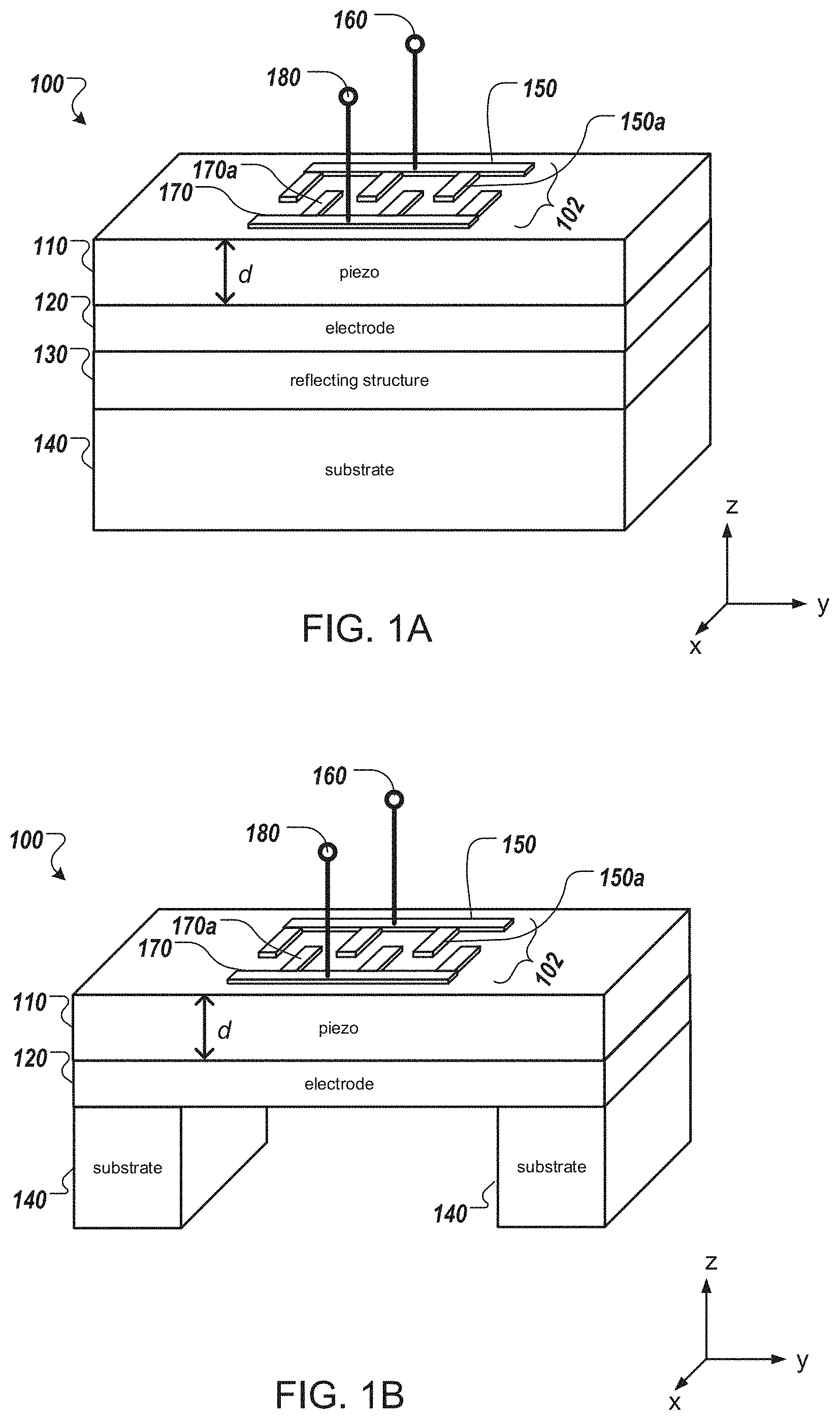
This specification relates to thin film radio-frequency acoustic wave filters. Radio-frequency (“RF”) components, such as resonators and filters, based on microacoustic and thin-film technology are widely used in radio applications such as: mobile phones, wireless networks, satellite positioning, etc. Their advantages over their lumped-element, ceramic, and electromagnetic counterparts include small size and mass-production capability. This specification describes technologies for band pass Lateral Bulk Acoustic Wave (“LBAW”) filters. More particularly, the present disclosure provides techniques to suppress sidebands in LBAW filters and improve band pass filter characteristic of LBAW filters. LBAWs can be used as band pass filters. The band pass filter may include one or more undesired (or parasitic) sidebands. Implementations of the present disclosure provide techniques to suppress the undesired sidebands by cascading two or more LBAWs. LBAW filters are formed from a piezoelectric layer sandwiched between two pairs of electrodes. One electrode from each pair is located on the top surface of the piezoelectric layer, and forms an input or an output of the LBAW. The input and output electrodes are separated by a gap. Each pair also has a counter electrode located on the bottom surface of the piezoelectric layer. By applying an alternating voltage across the piezoelectric layer at the input resonator, a mechanical resonance is formed in the piezoelectric layer below the input electrode. The piezoelectric layer thickness and the gap between electrodes can be designed such that this mechanical resonance is coupled across the gap to the output resonator. The frequency range at which such coupling occurs determines the achievable bandwidth (or width of passband) for the LBAW filter. In general, one innovative aspect of the subject matter described in this specification can be embodied in an acoustic wave filter device that includes an acoustic reflector, an intermediary layer providing or on a topmost layer of the acoustic reflector, a first multilayer stack on the acoustic reflector, and a second multilayer stack on the acoustic reflector and adjacent to the first multilayer stack. The intermediary layer has a first region and a second region, the first region having a first layer thickness and the second region having a second layer thickness different from the first layer thickness. The first multilayer stack includes a first counter electrode on the first region of the intermediary layer, and a first piezoelectric layer on the first counter electrode, and a first input electrode and a first output electrode on the first piezoelectric layer. The first input electrode and the first output electrode each has a first electrode thickness and extends substantially in parallel and separated by a first gap. The second multilayer stack includes a second counter electrode on the second region of the intermediary layer, a second piezoelectric layer on the second counter electrode, and a second input electrode and a second output electrode on the second piezoelectric layer. The second input electrode and the second output electrode each has a second electrode thickness and extends substantially in parallel and separated by a second gap. The first output electrode is electrically connected to the second input electrode. The first multilayer stack and second multilayer stack are configured such that application of a radio frequency voltage between the first input electrode and the first counter electrode layer creates acoustic modes in the piezoelectric layer between the first input and output electrodes and between the second input and output electrodes. In some examples, application of a radio frequency voltage between the first input electrode and the first counter electrode layer creates acoustic thickness-extensional resonance modes in the piezoelectric layer between the first input and output electrodes and between the second input and output electrodes The foregoing and other embodiments can each optionally include one or more of the following features, alone or in combination. The second layer thickness can be greater than the first layer thickness. For example, the second layer thickness can be 1% to 10% greater than the first layer thickness. The radio frequency voltage between the first input electrode and the first counter electrode layer can create second-order acoustic thickness-shear (TS2) resonance mode in the piezoelectric layer between the first input and output electrodes and between the second input and output electrodes. The second layer thickness can be different than the first layer thickness so that a first resonance frequency of TS2 resonance mode created between the first input and output electrodes of the first multilayer stack differs from a second resonance frequency of TS2 resonance mode created between the second input and output electrodes of the second multilayer stack. For example, the first resonance frequency can differ by 1% to 8% from the second resonance frequency. The first resonance frequency can differ from the second resonance frequency by at least 50 MHz. In some embodiments, the second electrode thickness is greater than the first electrode thickness. In some embodiments, the second electrode thickness is less than the first electrode thickness. For example, the second electrode thickness can be 1% to 10% thinner than the first electrode thickness. Each of the first input and output electrodes can have multiple first extensions. The multiple first extensions of the first input electrode can be interdigitated with the multiple first extensions of the first output electrode. Each of the second input and output electrodes can have with multiple second extensions. The multiple second extensions of the second input electrode can be interdigitated with the multiple second extensions of the second output electrode. In some examples, each of the first input and output electrodes is a comb structure having the multiple first extensions and each of the second input and output electrodes is a comb structure having the multiple second extensions. The multiple first extensions can be thicker than the multiple second extensions. For example, the second extension thickness can be 5% to 20% less than the first extension thickness. The second extension thickness can be greater than the first extension thickness so that a first resonance frequency of thickness-extensional (TE1) resonance mode created between the first input and output electrodes of the first multilayer stack is within 1% from a second resonance frequency of TE1 resonance mode created between the second input and output electrodes of the second multilayer stack. The multiple second extensions can be substantially parallel to the multiple first extensions. The multiple second extensions can form an angle greater than zero with respect to the multiple first extensions. The acoustic reflector can be a Bragg mirror. The first output electrode and the second input electrode can be parts of a common electrode shared between the first multilayer stack and the second multilayer stack. The first output electrode can be connected to the second input electrode through a conductive connector. In some examples, the conductive connector has a length extending parallel to long axis of the extensions of at least one of the first and the second multilayer stacks that is greater than a width of the extensions measured perpendicular to the long axis of the extensions. The first output electrode can be substantially parallel to the second input electrode. The subject matter described in this specification can be implemented in particular embodiments so as to realize one or more of the following advantages. Band pass filters described herein can improve the band pass response of LBAW filters, e.g., by suppressing parasitic sidebands. The suppression can be achieved at particular frequencies or over a range of frequencies. In addition, LBAW filters described herein can be simpler to fabricate as compared to conventional acoustic filters because an LBAW uses only a single piezoelectric layer as compared to two vertically stacked bulk acoustic wave (BAW) coupled resonator filters. The LBAW filters can also operate at higher frequencies as compared to surface acoustic wave (SAW) filters because the LBAW filter operation is determined more by piezoelectric layer thickness than interdigital transducer (IDT) electrode dimensions. In some embodiments, LBAW filters can also achieve a wider bandwidth than BAW filters. LBAW filters can perform as filters with a single lithographic patterning step as compared to close to 10 in BAW and can operate without reflectors needed in SAW, and thus in smaller size. The details of one or more embodiments of the subject matter of this specification are set forth in the accompanying drawings and the description below. Other features, aspects, and advantages of the subject matter will become apparent from the description, the drawings, and the claims. Like reference numbers and designations in the various drawings indicate like elements. Acoustic vibrations are created in piezo layer 110 by applying an oscillating (or alternating) input voltage across IDT electrode 150 and bottom counter electrode 120 at an input port 160. The applied voltage is transformed into a mechanical (e.g., acoustic) vibration via the piezoelectric effect. Under resonance conditions (e.g., with certain acoustic resonance modes, as detailed further below), this vibration can create a standing wave under input electrode 150 and an evanescent wave (with exponentially decaying amplitude) in the gap region 190. With appropriate selection of vibration frequencies and gap width G, the standing wave can be coupled mechanically across gap 190 from the piezo region under electrode 150 to piezo region under electrode 170 by the evanescent wave and create a similar standing wave in piezo layer 110 under electrode 170. The standing wave under electrode 170 results in an output signal voltage with the same frequency at an output port 180 via the reverse piezoelectric effect. The frequency range at which this coupling occurs in mechanical resonance with strong piezoelectric coupling forms the passband (or bandwidth) of LBAW filter 100. In some example, the frequency range is between 1.8 and 1.95 GHz. As discussed further below, the thicknesses and geometries, and spacing of the various layers of LBAW 100 can be tuned to change the RF response and passband of the filter. Throughout this disclosure, width and length are measured along axes parallel to the piezoelectric layer and thickness is measured along the axis perpendicular to the piezoelectric layer. A reflecting structure 130 can serve to isolate the vibration in piezo layer 110 from an underlying substrate 140 and to prevent acoustic leakage. The reflecting structure can be a stack of thin layers, for example, a Bragg reflector composed of alternating high and low acoustic impedance (“Zac”) material layers. The thickness of these layers can be designed such that the frequencies with and near the passband of LBAW filter are reflected back into piezo layer 110 and all other frequencies pass through the mirror. In some embodiments, LBAW 100 does not directly overlie substrate 140 (as shown in In some embodiments, as shown in Although Piezo layer 110 can be formed from various piezoelectric materials. Exemplary materials include ZnO, AlN, CdS, PZT, LiNbO3, LiTaO3, quartz, KNN, BST, GaN, Sc alloyed AlN, or the aforementioned materials doped or alloyed with an additional element. Doping can be used to improve or tailor electromechanical properties of piezo layer 110. As detailed further below, piezo layer thickness d is selected such that thickness-extensional modes near the frequencies of the desired bandwidth of the LBAW filter are produced in the piezo layer. In some embodiments, piezo layer thickness d is 20% to 50% of λz, or 30% to 45% of Az, where λzis the wavelength of the piezoelectric vibration in the thickness direction. In some embodiments, d is 1500 nm to 2500 nm, or 1800 to 2200 nm. Thin film IDT 102 can be composed of various materials. In some embodiments, IDT electrodes 150 and 170 are metal. For example, the electrode material can include Al, Mo, Pt, Cu, Au, Ag, Ti, W, Ir, Ru, or multilayers of metals and/or metals doped with additional materials, e.g. AlSi, AlSiCu, polysilicon, etc. Doping can be used to improve or tailor IDT electric or mechanical properties. Although Reflecting structure 130 can be composed of alternating layers of different materials. For example, reflecting structure 130 can include alternating layers of two of: tungsten (W), SiO2, silicon (Si), and carbon (C). For example, layers of high acoustic impedance include W, Mo, Ir, Al2O3, diamond, Pt, AlN, Si3N4. Layers of low acoustic impedance can include SiO2, glass, Al, Ti, C, polymers, or porous materials. Layer of Si provides an intermediate acoustic impedance. Various materials are suitable for the substrate 140, such as Si or SiO2or glass, sapphire, quartz. Substrate 140 materials can have high electrical resistivity. The substrate can have a thickness appropriate for RF applications, such as integration into mobile phone platforms. For example, the substrate can have a thickness less than 500 microns, or less than 200 microns. For example, Si wafers can be purchased with a thickness of 675 μm and thinned down to a achieve desired device thickness, e.g., for mobile platforms. Modeling of the acoustic response of LBAW 100 can provide guidance on how to tune the design parameters for individual elements of the structure to achieve desired bandpass properties. For example, LBAW 100 can be designed to have resonance modes at specific frequencies. In general, the geometry of various LBAW 100 components can be selected to achieve various acoustic properties. LBAW 100 properties can depend on the combination of these geometries, which may not be independent of one another. In piezoelectric layer 110, different bulk acoustic vibration modes can arise at different excitation frequencies f of input voltage (e.g., at port 160). Acoustic vibrations in piezo layer 110 can propagate laterally as Lamb waves (or plate waves), wherein particle motion lies in the plane that contains the direction of wave propagation and the plate normal (e.g., the z-axis in where N is an integer that indicates the order of the resonance. For the TE1 mode, As discussed further below, the width W of the electrodes and the gap G between electrodes can be designed such that TE1 mode standing waves with certain lateral wavelengths λ∥ are formed that can couple through their evanescent tails across gap G to create two mechanical resonant modes. Acoustic properties of an LBAW resonator 100 can be described with dispersion curves. Referring to as a function of frequency f. The first-order longitudinal (thickness extensional, TE1) vibration mode, in which the combined thickness of the piezoelectric layer d and the thickness of electrode(s) 150 or 170 contains approximately half a wavelength of the bulk vibration, λz/2, and the second-order thickness shear (TS2) mode, in which the bulk vibration is dominantly perpendicular to the thickness direction (z-axis in In some embodiments, LBAW 100 can be designed to produce Type 1 dispersion. For example, piezo layer 110 materials can be selected in which Type 1 dispersion can occur. For example, ZnO can be used. In another example, appropriate design of acoustic Bragg reflector 130 can help achieve Type 1 dispersion. For example, using Aluminum nitride (“AIN”) for piezo layer 110 can typically produce a Type 2 dispersion, where TE1 mode behaves non-monotonically having initially decreasing k∥ with increasing frequency f, and then increasing k∥ with increasing frequency f, (roughly similar to what is described in the dispersion curves of in In In the limit of infinitely small gap width G, λevenapproaches the total width from below. As shown in Referring to where fsymmand fasymmare the symmetric and antisymmetric eigenfrequencies, respectively, and f0=(fsymm+fasymm)/2 is the center frequency between the two modes. In some embodiments, increasing the number of extensions (e.g., 150 The odd lateral standing wave resonance in this structure, however, approaches or is slightly larger than: Additionally, or alternatively, in some embodiments, the total width of the structure K·W+K·G can be such that the highest-order mode trapped in the structure is the desired odd mode resonance. For example, K can be 31, W can be 3 μm, and G can be 2 μm. In some embodiments, the number of electrode extensions K is between 2 and 200, or between 10 and 60. In some embodiments, the length L of electrode extensions can be between 50 μm and 2000 μm, or between 70 μm and 500 μm. In some embodiments, the gap G is selected to allow coupling of the evanescent tails of standing waves formed under electrodes 150 and 170. For example, the gap G between electrode extensions can be 0.1 μm and 10 μm, or between 2 μm and 5 μm. In some embodiments, the topology of the electrodes 150 and 170 can be designed such that the gap width G provides good enough coupling between electrode extensions to create a single even mode 410 across the entire width of the structure. For example, the gap width G can be 2%-300%, or 10%-100% of the evanescent acoustic wave's decay length, i.e. the length at which amplitude A=A0·e−1of the original amplitude A0, in the gap at the desired even resonance mode. The gap width G can be optimized. Decreasing the gap to a too small width (1) can eventually pull the even and odd modes too far from each other creating a dip in the passband, (2) can lead to reduced coupling coefficient for the odd mode, or (3) can increase capacitive feedthrough from finger to finger causing poor out of band attenuation. In some embodiments, the gap width G can be defined with respect to piezo layer thickness d. For example, G can be designed to be 10% to 300% of d, or 25% to 150% of d. In some embodiments, the width of electrode extensions W can be between 0.1 μm and 30 μm or between 2 μm and 5 μm. In some embodiments, W can be designed such that the wavelength λ∥ of the lateral acoustic wave at the desired odd mode resonance frequency λoddis obtained. In some embodiments, the electrode width W is designed such that multiple half-wavelengths cannot fit within the electrode width. For example, W can be designed to be smaller than the lateral acoustic wave's wavelength λ∥ at the desired odd resonance mode, e.g., where λ∥=λodd. In some embodiments, the thicknesses of various LBAW 100 components can be selected to achieve various acoustic properties and may be interdependent. For example, the piezo layer 110 thickness d (minimum and maximum value) can first be determined with respect to the acoustic wavelength in the piezo material (λ) at the operation frequency f. In some embodiments, thicknesses (min and max) of the other LBAW 100 layers can be selected based on the choice of piezo thickness d. For example, the combined thickness of the electrodes (including the counter electrode 120) and the piezoelectric layer can be selected to be approximately half a wavelength of the mode that is being used, for example longitudinal bulk wave for the thickness extensional mode. Fundamental modes with N=1 (the first mode, i.e., first harmonic) can allow for greater coupling, but N>1 modes are also possible. For example, the thickness of electrodes 150 and 170, bottom electrode 120, and reflecting structure 130 can be defined as a percentage of piezo layer thickness d. In some embodiments, once all thicknesses are selected, the geometry of the electrode extensions 150 In some embodiments, thickness of electrodes 150 and 170 is between 1% to 30% of d, or 5% to 25% of d, or 3% to 15% of d. In some embodiments, the thickness of bottom electrode 120 is between 5% to 50% of d, or 10% to 30% of d, or 10% to 20% of d. In some embodiments, where the reflecting structure 130 is a Bragg reflector, the alternative layers of the reflector can be designed such that the required reflectivity of passband wavelengths is obtained. For example, the thickness of each layer can be equal to or less or more than one quarter of the acoustic wavelength A in the thickness direction to reflect the odd and even TE1 resonance modes. In some embodiments, a single layer in the Bragg reflector can be 15% to 80% of d, or 20% to 70% of d. The mass loading of the IDT 102, determined by the thickness and material of electrodes 150 and 170, can be designed such that the frequency difference between the k∥=0 frequency of the electrode region's TE1 mode and the outside electrode region's TS2 mode is small. Without wishing to be bound by any particular theory, when the frequency difference between outside region's TS2 mode and electrode region's TE1 mode is small, the trapping range is large. More particularly, the k∥=0 frequency of the outside region's TS2 mode can be 95%-99% of the electrode region's TE1 cutoff frequency. The frequency difference between the outside region's TS2 and outside region's TE1 modes' k∥=0 frequencies is designed to be large, e.g. 5%-15%, for example 6.5%-7.5%, of the electrode region's TE1 mode cutoff frequency. According to certain embodiments of the present invention, the k=0 frequency of the outside region's TS2 mode is greater than, or equal to 98%, or between 98% and 99.5%, or is 98.9% of the electrode region's TE1 cutoff frequency. Similarly, the frequency distance expressed as the frequency difference between electrode region TE1 and outside region TS2 k∥=0 frequencies: should be small, for example on the order of 1%. As an example, said frequency distance can be between 0.2% and 2.1%, or between 0.5% and 1.8%, or between 0.8% and 1.5%, or for example, 1.1%. In some embodiments, LBAW 100 can be designed to have a passband for TE1 modes between 0.5 and 10 GHz, or between 1 and 4 GHz. In some examples, TE1 passband is between 1.8 and 3.7 GHz. The limits of the passband can incorporate design considerations. For example, the dimensions of the device can grow very large or very small. Too large dimensions may take too much space and cause inefficiencies. Too small dimensions can deteriorate performance due to thin and narrow electrodes leading to resistance and losses. In some embodiments, LBAW 100 can be designed to have a TE1 passband width 510 Implementations of the present disclosure provides techniques to suppress LBAW sidebands created by TS2 mode. The implementations suppress the sidebands by cascading multiple LBAWs. The cascaded LBAW filters can be designed to have different TS2 resonance frequencies so that insertion loss of one filter suppresses sideband of the other filter. Electrode 150 is an input electrode and electrode 170 is an output electrode of the first LBAW 100 In some embodiments, electrode 170 is connected to electrode 670 through a conductive connector 660. Alternatively, as shown in The conductive connector 660 can have up to the same length as the electrodes 170, 670 (measured along the long axis of the electrodes 170, 670, e.g., perpendicular to the long axis of the extensions 170 In some embodiments, a filter device may have no conductive connector 660, as depicted in In some embodiments, the common electrode 602 consists of individual fingers; the fingers do not extend from a conductive base and need not be electrically connected. The electrodes 150, 650, and the common electrode 602 (that provide the base of the comb structures) are spaced apart. The electrodes 170, 670, 602 can be rectangular bodies, and can extend substantially in parallel (i.e., their long axes are substantially parallel). Alternatively, electrodes 150 and 170 can be arranged to form an angle greater than zero with respect to electrodes 650 and 670. Two opposing electrodes (as parts of one LBAW or as parts of the common electrode 602) can have similar or different shapes and/or dimensions. Each of the electrodes 150, 170, 650, 670 includes two or more extensions 150 In each of the first and the second LBAWs 100 The two LBAWs 100 Two interdigitated comb structures within an LBAW can have the same or different number of extensions. For example, as shown in Rather than two comb structures, a filter device may include a first electrode that provides a comb structure with multiple extensions, and a second electrode that includes a single bar-shaped conductive body (e.g., a single extension) extending between the extensions of the comb. The comb structure is integrated by the bar extension. The electrodes 150, 170, 650, 670 can be composed of the same or different materials. The extensions 150 The first LBAW 100 Similarly, the second LBAW 100 The first and/or the second intermediary layers can be two regions of an intermediary layer. The intermediary layer can be the topmost layer of the acoustic reflector 608 or can be positioned on top of the topmost layer of the acoustic reflector. The two regions that include the first and the second intermediary layers can have different thicknesses. The acoustic reflector 608 can have one or more layers. The topmost layer of the acoustic reflector 608 is a layer that is closest to the counter electrode from among the layers of the acoustic reflector 608. In some embodiments, the first and/or the second reflector is a Bragg mirror. The first and the second reflectors 608 and 618 can be parts of a common reflector shared between the first and the second LBAWs 100 Cascaded LBAWs can be utilized to suppress spurious sidebands created by TS modes. For example, embodiment 600 may have a sideband that is a result of sidebands of the first and the second LBAWs 100 Resonance frequencies corresponding to TE1 mode (fTE1) and Resonance frequency corresponding to TS2 mode (fTS2) of an LBAW depend on geometry and characteristics of the layers of the LBAW. The resonance frequency ratio fTE1/fTS2of an LBAW is a function of the Poisson ratio of the materials used in the LBAW. The Poisson ratio of a multilayer structure with a stack of two materials A and B is a function of tA/tB, where tAis thickness of a layer composed of material A, and tBis thickness of a layer composed of material B. Accordingly, resonance frequency ratio fTE1/fTS2of an LBAW depends on thickness of the LBAW's layers with respect to each other and can be adjusted by changing thickness of one or more layers of the LBAW. For example, resonance frequency ratio of an LBAW can be adjusted by changing thickness of dielectric layer, piezo layer, etc. of the LBAW. Thus, the two LBAWs 100 The first and the second intermediary layer 606, 616 can be composed of the same material, e.g., silicon oxide (SiO2), silicon nitride (SiN), etc. However, as described further below, the first and the second intermediary layer 606, 616 can have different thicknesses. In the example embodiments depicted in To tune TS2 resonance frequency of the first LBAW 100 In the present disclosure, the two intermediary layers are fabricated so that one intermediary layer is thicker than the other intermediary layer. For example, the intermediary dielectric layer 616 can be thicker than the first intermediary layer 606 (as shown in As illustrated, the sideband 732 of the cascaded LBAWs is suppressed compared to the passband 740. In particular, the sideband 732 can have more than 30 dB loss, whereas the passband is less than 10 dB loss. Similarly, the sideband 732 of the cascaded LBAWs is suppressed compared to each of the sidebands 712 and 722 associated with the individual LBAWs; the sideband peaks 730 As explained above, the second intermediary layer 616 can be thicker or thinner than the first dielectric layer 606. In the example depicted in In some embodiments, the thickness difference of the two intermediary layers 606 and 616 causes a 1 to 10% difference between the resonance frequencies of TS2 modes (i.e., frequencies of the sideband peaks 710 To make sure that the TE1 passband of the second LBAW 100 In the example embodiment depicted in Further, TE1 resonance frequencies can be tuned by selecting appropriate IDT geometries, such as width of the extensions, gap between the extensions, or the number of extensions of at least one of the LBAWs. For example, when the second dielectric layer 616 is thicker than the first dielectric layer 606, the extension width and/or gap between the extensions in the second LBAW 100 In some embodiments, to adjust the TE1 passbands of the two LBAWs 100 A number of implementations have been described. Nevertheless, it will be understood that various modifications may be made without departing from the spirit and scope of disclosure. Accordingly, other implementations are within the scope of the following claims. Acoustic wave filter devices are disclosed. A device includes a layer providing or on a topmost layer of an acoustic reflector. The intermediary layer has a first region and a second region. The first region has a first layer thickness and the second region has a second layer thickness different from the first layer thickness. The device includes a first multilayer stack on the first region and a second multilayer stack on the second region of the intermediary layer. Each of the first and the second stacks includes a piezoelectric layer on a counter electrode that is located on the respective region, an input and an output electrode. Application of a radio frequency voltage between the input electrode and the counter electrode layer of the first stack creates acoustic resonance modes in the piezoelectric layer between the input and output electrodes of the first and the second stack. 1. An acoustic wave filter device comprising:
an acoustic reflector comprising one or more layers; an intermediary layer providing or on a topmost layer of the acoustic reflector, wherein the intermediary layer has a first region and a second region, the first region having a first layer thickness and the second region having a second layer thickness different from the first layer thickness; a first multilayer stack on the acoustic reflector comprising
a first counter electrode on the first region of the intermediary layer, a first piezoelectric layer on the first counter electrode, and a first input electrode and a first output electrode on the first piezoelectric layer, the first input electrode and the first output electrode each having a first electrode thickness and extending substantially in parallel and separated by a first gap; and a second multilayer stack on the acoustic reflector comprising
a second counter electrode on the second region of the intermediary layer, a second piezoelectric layer on the second counter electrode, and a second input electrode and a second output electrode on the second piezoelectric layer, the second input electrode and the second output electrode each having a second electrode thickness and extending substantially in parallel and separated by a second gap, wherein the first output electrode is electrically connected to the second input electrode, and wherein the first multilayer stack and second multilayer stack are configured such that application of a radio frequency voltage between the first input electrode and the first counter electrode creates acoustic thickness-extensional resonance modes in the piezoelectric layer between the first input and output electrodes and between the second input and output electrodes. 2. The device of 3. The device of the second layer thickness is different than the first layer thickness so that a first resonance frequency of TS2 resonance mode created between the first input and output electrodes of the first multilayer stack differs from a second resonance frequency of TS2 resonance mode created between the second input and output electrodes of the second multilayer stack. 4. The device of 5. The device of 6. The device of 7. The device of 8. The device of 9. The device of 10. The device of 11. The device of 12. The device of 13. The device of 14. The device of 15. The device of 16. The device of 17. The device of 18. The device of 19. The device of 20. The device of 21. The device of 22. An acoustic wave filter device comprising:
an acoustic reflector comprising one or more layers; an intermediary layer providing or on a topmost layer of the acoustic reflector, wherein the intermediary layer has a first region and a second region, the first region having a first layer thickness and the second region having a second layer thickness different from the first layer thickness; a first multilayer stack on the acoustic reflector comprising
a first counter electrode on the first region of the intermediary layer, a first piezoelectric layer on the first counter electrode, and a first input electrode and a first output electrode on the first piezoelectric layer, the first input electrode and the first output electrode each having a first electrode thickness and extending substantially in parallel and separated by a first gap; and a second multilayer stack on the acoustic reflector comprising
a second counter electrode on the second region of the intermediary layer, a second piezoelectric layer on the second counter electrode, and a second input electrode and a second output electrode on the second piezoelectric layer, the second input electrode and the second output electrode each having a second electrode thickness and extending substantially in parallel and separated by a second gap, wherein the first output electrode is electrically connected to the second input electrode, and wherein the first multilayer stack and second multilayer stack are configured such that application of a radio frequency voltage between the first input electrode and the first counter electrode layer creates acoustic modes in the piezoelectric layer between the first input and output electrodes and between the second input and output electrodes.BACKGROUND
Technical Field
Background
SUMMARY
BRIEF DESCRIPTION OF THE DRAWINGS
DETAILED DESCRIPTION