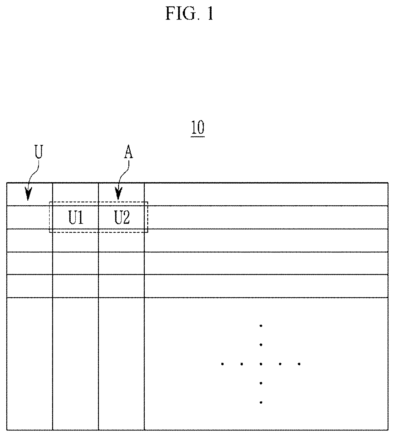
COMBINATION STRUCTURES AND OPTICAL FILTERS AND IMAGE SENSORS AND CAMERA MODULES AND ELECTRONIC DEVICES
This application claims priority to and the benefit of, under 35 U.S.C. § 119, Korean Patent Application No. 10-2019-0109005 filed in the Korean Intellectual Property Office on Sep. 3, 2019, the entire contents of which are incorporated herein by reference. Combination structures, optical filters, image sensors, camera modules, and electronic devices are disclosed. Electronic devices including image sensors that store an image as an electrical signal, such as a cell phone, a digital camera, a camcorder, or a camera, have been used. These electronic devices may include an optical filter in order to reduce or prevent an optical distortion by light in the other regions (e.g., other wavelength spectra) than a visible wavelength spectrum or improve visibility by light in the other wavelength spectra than a visible wavelength spectrum. Some example embodiments provide a combination structure capable of achieving desired optical properties for light except for visible wavelength regions (“wavelength regions” or “regions” being referred to interchangeably herein as “wavelength spectra”) with a thin thickness. Some example embodiments provide an optical filter including the combination structure. Some example embodiments provide an image sensor including the combination structure or the optical filter. Some example embodiments provide a camera module including the combination structure, the optical filter or the image sensor. Some example embodiments provide an electronic device including the combination structure, the optical filter, the image sensor, or the camera module. According to some example embodiments, a combination structure may include an in-plane pattern of unit cells, wherein each unit cell of the unit cells includes nanostructures each having a dimension that is smaller than a near-infrared wavelength, and a light-absorbing layer adjacent to the nanostructures, the light-absorbing layer including a near-infrared absorbing material configured to absorb light in at least a portion of a near-infrared wavelength spectrum. The nanostructures may define a nanostructure array in the unit cells. A wavelength width at 50% transmittance of a transmission spectrum in the near-infrared wavelength spectrum of the combination structure may be wider than a wavelength width at 50% transmittance of a transmission spectrum in the near-infrared wavelength spectrum of the nanostructure array. The transmission spectrum in the near-infrared wavelength spectrum of the nanostructure array may have a first local minimum point and a second local minimum point separated from each other and a first local maximum point between the first local minimum point and the second local minimum point, and a difference between a transmittance at either the first local minimum point or the second local minimum point and a transmittance at the first local maximum point may be greater than about 30%. The transmission spectrum in the near-infrared wavelength spectrum of the combination structure may have a third local minimum point and a fourth local minimum point separated from each other and a second local maximum point between the third local minimum point and the fourth local minimum point, and a difference between a transmittance at either the third local minimum point and the fourth local minimum point and a transmittance at the second local maximum point may be smaller than the difference between the transmittance at either the first local minimum point or the second local minimum point and the transmittance at the first local maximum point. The difference between the transmittance at either the third local minimum point and the fourth local minimum point and the transmittance at the second local maximum point may be less than about 30%. The nanostructure array may include a parallel pattern of a first nanostructure, a second nanostructure, and a third nanostructure, and a magnitude of a gap between the first nanostructure and the second nanostructure may differ from a magnitude of a gap between the second nanostructure and the third nanostructure. The gap between the first nanostructure and the second nanostructure may be about 1.05 times to about 5 times as large as the gap between the second nanostructure and the third nanostructure. The nanostructure array may include a first nanostructure and a second nanostructure which are adjacent to each other and a dimension of the first nanostructure may be different from a dimension of the second nanostructure. A width of the first nanostructure may be about 1.05 times to 5 times as large as a width of the second nanostructure. A thickness of the first nanostructure may be about 1.05 times to 5 times as large as a thickness of the second nanostructure. The unit cells may include a first unit cell and a second unit cell which are adjacent to each other, the first unit cell may include a first nanostructure and a second nanostructure, the second unit cell may include a third nanostructure and a fourth nanostructure, the first nanostructure, the second nanostructure, the third nanostructure, and the fourth nanostructure may define a linear sequence of nanostructures extending in one direction, and a magnitude of a gap between the first nanostructure and the second nanostructure may differ from a magnitude of a gap between the second nanostructure and the third nanostructure. The gap between the first nanostructure and the second nanostructure may be about 0.2 times to about 0.9 times or about 1.05 times to about 5 times as large as a gap between the second nanostructure and the third nanostructure. A wavelength width at the 50% transmittance of the transmission spectrum in the near-infrared wavelength spectrum of the combination structure may be about 1.2 times to 5 times as large as a wavelength width at the 50% transmittance of the transmission spectrum in the near-infrared wavelength spectrum of the nanostructure array. A wavelength width at the 50% transmittance of the transmission spectrum in the near-infrared wavelength spectrum of the combination structure may be about 40 nm to about 200 nm. The light-absorbing layer may be at at least one of a lower surface, an upper surface, and/or one or more side surfaces of one or more nanostructures of the nanostructures. The nanostructure and the light-absorbing layer may be in contact with each other. The near-infrared wavelength may be in a range of greater than about 700 nm and less than or equal to about 1200 nm. The near-infrared wavelength may be in a range of about 890 nm to about 990 nm. The nanostructures may each include a high refractive material having a refractive index of greater than or equal to about 2.0 at a wavelength of 940 nm. The nanostructure may each include titanium oxide, silicon, aluminum, a Group III-V semiconductor compound, or a combination thereof. A maximum absorption wavelength of the near-infrared absorbing material may be in a range of about 890 nm to about 990 nm. A thickness of the combination structure may be less than or equal to about 1 μm. According to some example embodiments, a combination structure may include an in-plane pattern of unit cells. Each unit cell of the unit cells may include two or more nanostructures each having a smaller dimension than a near-infrared wavelength, and a light-absorbing layer adjacent to at least one of a lower surface, an upper surface, and/or one or more side surfaces of one or more nanostructures of the two or more nanostructures, the light-absorbing layer including a near-infrared absorbing material configured to absorb light of at least a portion of a near-infrared wavelength spectrum. The unit cells may include a first unit cell and a second unit cell adjacent to each other. The first unit cell may include a first nanostructure and a second nanostructure. The second unit cell may include a third nanostructure and a fourth nanostructure. The first nanostructure, second nanostructure, third nanostructure, and fourth nanostructure may define a linear sequence of nanostructures extending in one direction. A dimension of the first nanostructure may be different from a dimension of the second nanostructure, or a magnitude of a gap between the first nanostructure and the second nanostructure may be different from a magnitude of a gap between the second nanostructure and the third nanostructure. The dimension of the first nanostructure may be different from the dimension of the second nanostructure, and the width of the first nanostructure may be about 1.05 times to about 5 times as large as the width of the second nanostructure. The gap between the first nanostructure and the second nanostructure may differ from the gap between the second nanostructure and the third nanostructure, and the gap between the first nanostructure and the second nanostructure may be about 0.2 times to about 0.9 times or about 1.05 times to about 5 times as large as the gap between the second nanostructure and the third nanostructure. According to some example embodiments, an optical filter including the combination structure is provided. According to some example embodiments, a camera including the optical filter is provided. According to some example embodiments, an image sensor may include a semiconductor substrate including a plurality of photodiodes and an optical filter on the semiconductor substrate and configured to block light in at least a portion of near-infrared wavelength spectra, wherein the optical filter includes the combination structure. The image sensor may further include a color filter on the optical filter. According to some example embodiments, a camera includes the image sensor. According to some example embodiments, an electronic device includes the optical filter, the image sensor or the camera. Desired optical properties for light in near-infrared wavelength spectra with a thin thickness may be effectively implemented. Hereinafter, example embodiments will be described in detail so that a person skilled in the art would understand the same. This disclosure may, however, be embodied in many different forms and is not construed as limited to the example embodiments set forth herein. In the drawings, the thickness of layers, films, panels, regions, etc., are exaggerated for clarity. Like reference numerals designate like elements throughout the specification. It will be understood that when an element such as a layer, film, region, or substrate is referred to as being “on” another element, it can be directly on the other element or intervening elements may also be present. In contrast, when an element is referred to as being “directly on” another element, there are no intervening elements present. Hereinafter, a combination structure according to some example embodiments is described with reference to drawings. A combination structure 10 according to some example embodiments includes a plurality of unit cells (U) arranged repeatedly along an in-plane direction, for example a plurality of unit cells (U) are regularly or periodically along rows and/or columns. For example, the combination structure 10 may include a plurality of unit cells arranged repeatedly or periodically (e.g., in a pattern) in a plane to establish an in-plane (e.g., two-dimensional) pattern (e.g., “array”) of unit cells (U). A plurality of unit cells (U) arranged repeatedly in one or more in-plane directions may be referred to herein interchangeably as an in-plane pattern of unit cells (U), where said in-plane pattern may include at least one row pattern and/or column pattern of unit cells (U) and/or an array of unit cells (U) arranged in at least one row and/or at least one column (e.g., a plurality of rows and a plurality of columns). Each unit cell (U) includes one or more three-dimensional nanostructures 11 In some example embodiments, each unit cell (U) may include two or more nanostructures 11 In some example embodiments, a unit cell (U) includes a plurality of nanostructures 11 The nanostructures 11 When the terms “about” or “substantially” are used in this specification in connection with a numerical value, it is intended that the associated numerical value include a tolerance of ±10% around the stated numerical value. When ranges are specified, the range includes all values therebetween such as increments of 0.1%. The one or more nanostructures 11 The plurality of nanostructures 11 The nanostructure array 11 and/or the nanostructures 11 The nanostructure array 11 may be configured to reflect or absorb light of a particular (or, alternatively, predetermined) wavelength belonging to a near-infrared wavelength spectrum (e.g., a particular near-infrared wavelength spectrum), wherein one or more dimensions of the nanostructures 11 The width (W) of the nanostructures 11 The thickness (t) of the nanostructures 11 The gap (g) of the nanostructures 11 The period (p) of the nanostructures 11 The nanostructure array 11 includes a plurality of nanostructures 11 In some example embodiments, at least one nanostructure 11 In some example embodiments, a width (W1) of the first nanostructure 11 In some example embodiments, a thickness (t1) of the first nanostructure 11 In some example embodiments, a gap (g) between two nanostructures 11 As described herein, where any dimension is described to be different from any other dimension (e.g., gap (g1) being different from gap (g2) as described above), it will be understood that the magnitude of the dimension may be different from the magnitude of the other dimension (e.g., the magnitude of gap (g1) may be different from the magnitude of gap (g2)). As shown in In some example embodiments, the gap (g1) between the first nanostructure 11 In some example embodiments, the gap (g1) between the first nanostructure 11 However, it is not limited thereto, and when at least three nanostructures 11 In some example embodiments, a period (p) between two nanostructures 11 In some example embodiments, a dimension, for example a width (W) and/or a thickness (t) of at least one nanostructure 11 In this way, a portion of the nanostructures 11 In some example embodiments, a transmission spectrum and a reflection spectrum of the nanostructure array 11 having consistent dimension and alignment of the nanostructures 11 In this way, the transmission spectrum and the reflection spectrum of the nanostructure array 11 have two or more separate peaks in the particular (or, alternatively, predetermined) near-infrared wavelength spectrum and thus may widen a wavelength width exhibiting particular (or, alternatively, predetermined) transmittance and reflectance compared with the spectra having a single peak. Referring to Herein, the transmittance at the local minimum points (M1and M2) and transmittance at the local maximum point (M3) may have a relatively large difference. In some example embodiments, the difference between the transmittance at one of the local minimum points (e.g., either M1or M2) and the transmittance of the local maximum point (M3) may be larger (‘greater”) than about 30%, greater than about 30% and less than or equal to about 80%, about 40% to about 80%, about 40% to about 70%, or about 40% to about 60%. In some example embodiments, the transmittance at the local minimum points (M1and M2) may be less than or equal to about 10%, less than or equal to about 5%, less than or equal to about 3%, less than or equal to about 2%, less than or equal to about 1%, less than or equal to about 0.5%, or about 0%, and the transmittance at the local maximum point (M3) may be greater than about 10%, greater than about 10% and less than or equal to about 80%, about 15% to about 80%, about 20% to about 80%, about 25% to about 80%, about 30% to about 70%, about 35% to about 70%, about 40% to about 70%, or about 45% to about 70%. In some example embodiments, when absorptance of the nanostructure array 11 in a near-infrared wavelength spectrum is substantially 0, a reflection spectrum R1of the nanostructure array 11 in the near-infrared wavelength spectrum may be symmetrical to a transmission spectrum (T1), and the reflection spectrum R1has two separate local maximum points (M4and M5) and a local minimum point (M6) between the two separate local maximum points (M4and M5). The nanostructure array 11 according to some example embodiments may have a modified optical spectrum and widen a wavelength showing particular (or, alternatively, predetermined) transmittance compared with a nanostructure array 11 having consistent dimension and alignment of the nanostructures 11 The light-absorbing layer 12 may be configured to absorb light of a particular (or, alternatively, predetermined) wavelength. As shown in at least The light-absorbing layer 12 includes a light-absorbing material configured to absorb light of a particular (or, alternatively, predetermined) wavelength. The light-absorbing material may be one or more of an organic material, an inorganic material, organic/inorganic material, or a combination thereof. In some example embodiments, the light-absorbing layer 12 may include a near-infrared absorbing material configured to absorb light in at least a portion of near-infrared wavelength spectra. As described herein, “wavelength spectra” may include one or more wavelength spectra and may include a single wavelength spectrum, and in some example embodiments the light-absorbing layer 12 may include a near-infrared absorbing material configured to absorb light in at least a portion of the near-infrared wavelength spectrum, which may be the same near-infrared wavelength spectrum that includes a near-infrared wavelength that is larger than one or more dimensions of the unit cells. For example, the near-infrared absorbing material may be configured to absorb light in at least a portion of a wavelength spectrum of greater than about 700 nm and less than or equal to about 1200 nm and a maximum absorption wavelength (λmax,A) of the near-infrared absorbing material may for example belong to a range of greater than about 700 nm and less than or equal to about 1100 nm, greater than about 700 nm and less than or equal to about 1000 nm, about 750 nm to about 1100 nm, about 750 nm to about 1000 nm, about 800 nm to about 1000 nm, about 850 nm to about 990 nm, about 870 nm to about 990 nm, or about 890 nm to about 990 nm. The near-infrared absorbing material may be one or more materials, and is not particularly limited as long as it is configured to selectively absorb light in a near-infrared wavelength spectrum. The near-infrared absorbing material may be an organic material, an inorganic material, an organic/inorganic material, and/or a combination thereof. The near-infrared absorbing material may include for example a quantum dot, a quinoid metal complex compound, a polymethine compound, a cyanine compound, a phthalocyanine compound, a merocyanine compound, a naphthalocyanine compound, an immonium compound, a diimmonium compound, a triarylmethane compound, a dipyrromethene compound, an anthraquinone compound, a diquinone compound, a naphthoquinone compound, a squarylium compound, a rylene compound, a perylene compound, a pyrylium compound, a squaraine compound, a thiopyrylium compound, a diketopyrrolopyrrole) compound, a boron-dipyrromethene compound, a nickel-dithiol complex compound, a croconium compound, a derivative thereof, or a combination thereof, but is not limited thereto. In some example embodiments, the light-absorbing layer 12 including the near-infrared absorbing material may have a refractive index (n) in a near-infrared wavelength spectrum in a range of less than about 2.0, less than or equal to about 1.9, or less than or equal to about 1.8, for example greater than or equal to about 1.1 and less than about 2.0, about 1.1 to about 1.9, or about 1.1 to about 1.8. In some example embodiments, an average refractive index (n) at a wavelength spectrum of about 900 nm to about 1000 nm (e.g., 940 nm) may be less than about 2.0, less than or equal to about 1.9, or less than or equal to about 1.8, for example greater than or equal to about 1.1 and less than about 2.0, about 1.1 to about 1.9, or about 1.1 to about 1.8. In some example embodiments, the light-absorbing layer 12 including the near-infrared absorbing material may have an extinction coefficient (k) in the near-infrared wavelength spectrum of about 0.001 to about 0.5, for example an extinction coefficient (k) in a wavelength spectrum of about 900 nm to about 1000 nm (e.g., 940 nm) of about 0.01 to about 0.5. The light-absorbing layer 12 may be formed from a composition including the aforementioned near-infrared absorbing material, in some example embodiments, a curing product of the composition. The composition may optionally further include a binder, in addition to the aforementioned near-infrared absorbing material. The binder may be for example an organic binder, an inorganic binder, an organic/inorganic binder, or a combination thereof, and is not particularly limited as long as it is a material capable of mixing with the near-infrared absorbing material, dispersing in the near-infrared absorbing material, or binding the near-infrared absorbing materials. The binder may be a curable binder, for example a thermally curable binder, a photo-curable binder, or a combination thereof. The binder may be for example a (meth)acrylic binder, methyl cellulose, ethyl cellulose, hydroxypropyl methyl cellulose (HPMC), hydroxylpropyl cellulose (HPC), xanthan gum, polyvinyl alcohol (PVA), polyvinyl pyrrolidone (PVP), a cyclic olefin polymer (COP), carboxy methyl cellulose, hydroxyl ethyl cellulose, silicone, an organic-inorganic hybrid material, a copolymer thereof, or a combination thereof, but is not limited thereto. The near-infrared absorbing material may be for example included in an amount of about 0.01 to about 50 parts by weight, about 0.01 to about 30 parts by weight, about 0.01 to about 20 parts by weight, about 0.01 to about 15 parts by weight, or about 0.01 to about 10 parts by weight based on 100 parts by weight of the binder. The composition may optionally further include a solvent, in addition to the aforementioned near-infrared absorbing material, and binder. The composition may be coated on the base layer 13 that will be described later, dried, and then optionally cured. The coating may be for example a spin coating, a slit coating, a bar coating, a blade coating, a slot die coating, and/or an inkjet coating. The drying may be for example performed by natural drying, hot air drying, and/or a heat treatment at a higher temperature than the boiling point of the aforementioned solvent. The curing may be thermal curing, photo curing, or a combination thereof. The light-absorbing layer 12 may have a thickness 12 The base layer 13 is disposed under the nanostructure array 11 and the light-absorbing layer 12 and may support the nanostructure array 11 and the light-absorbing layer 12. The base layer 13 may be a transparent base layer and, in some example embodiments, have transmittance of greater than or equal to about 85% or greater than or equal to about 90% in a wavelength spectrum of about 400 nm to about 1000 nm. The base layer 13 may have a lower refractive index than that of the nanostructures 11 The combination structure 10 may have a thickness 10 The combination structure 10 may exhibit high light absorption characteristics at a thin thickness by combining the nanostructure array 11 and the light-absorbing layer 12. This is based on unique optical properties of the nanostructure array 11 called to be a metamaterial or a metastructure, and the nanostructure array 11 and/or the nanostructures 11 An amount of the multi-absorbed light may be greatly higher than an amount of the absorbed light in a structure without nanostructure array 11, in which incident light from a structure having no nanostructure array 11, that is, a planar structure once passes the light-absorbing layer 12. In addition, as described above, a portion of the nanostructures 11 The combination structure 10 may stably decrease transmittance and reflectance and increase absorptance in a relatively wide wavelength width due to the complementary combination of the nanostructure array 11 and the light-absorbing layer 12. The light-absorbing layer 12 may be configured to absorb light in a wavelength spectrum between two separate peaks in the transmission spectrum of the above nanostructure array 11 and thus decrease transmittance but increase absorptance in a wide wavelength width in a near-infrared wavelength spectrum of the combination structure 10. Ultimately, the combination structure 10 may decrease transmittance but increase absorptance in a wide range of the near-infrared wavelength spectrum and thus effectively block light in the near-infrared wavelength spectrum. Referring to In some example embodiments, a wavelength width (W2) at 50% transmittance in a near-infrared wavelength spectrum (e.g., the same particular near-infrared wavelength spectrum that the near-infrared absorbing material of the light-absorbing layer 12 is configured to absorb light in at least a portion thereof) of the transmission spectrum (T2) of the combination structure 10 may be wider than a wavelength width (W1) at 50% transmittance in the near-infrared wavelength spectrum of the transmission spectrum (T1) of the nanostructure array 11, in some example embodiments, about 1.2 times to about 10 times and within the range, about 1.2 times to about 5 times or about 1.2 times to about 3 times as large as the wavelength width (W1) at 50% transmittance in the near-infrared wavelength spectrum of the transmission spectrum (T1) of the nanostructure array 11. In some example embodiments, the wavelength width (W2) at the transmittance of 50% in the near-infrared wavelength spectrum of the transmission spectrum (T2) of the combination structure 10 may be about 38 nm to about 200 nm and within the range, about 40 nm to about 200 nm, about 40 nm to about 180 nm, or about 43 nm to about 150 nm. In some example embodiments, the transmission spectrum (T2) of the combination structure 10 in the near-infrared wavelength spectrum also may have two separate peaks, in some example embodiments, two separate local minimum points (Q1and Q2) and a local maximum point (Q3) between the two separate local minimum points (Q1and Q2) like the transmission spectrum (T1) of the nanostructure array 11 in the near-infrared wavelength spectrum. Restated, the transmission spectrum (T1) of the combination structure 10 may have a first local minimum point (a) and a second local minimum point (Q2) separated from each other, and a first local maximum point (Q3) between the first local minimum point (a) and the second local minimum point (Q2) Herein, the local minimum points (Q1and Q2) may be inflection points having lower transmittance than neighboring wavelength spectra, and the local maximum point (Q3) may be an inflection point having higher transmittance than the neighboring wavelength spectra. Minimum transmittance of the combination structure 10 may be transmittance at one of the local minimum points (Q1or Q2). As described above, the light-absorbing layer 12 may be configured to absorb light in a wavelength spectrum between two separate peaks in the transmission spectrum of the above nanostructure array 11, and accordingly, a transmittance difference between at one of the local minimum points (e.g., at either Q1or Q2) of the combination structure 10 and at the local maximum point (Q3) may be smaller than a transmittance difference between at one of the local minimum points (M1or M2) of the nanostructure array 11 and at the local maximum point (M3). In some example embodiments, the transmittance difference between at one of the local minimum points (Q1or Q2) of the combination structure 10 and at the local maximum point (Q3) may be less than or equal to about 30%, about 0 to about 30%, about 0.1% to about 30%, about 3% to about 30%, about 5% to about 30%, about 5% to about 20%, or about 5% to about 10%. When the transmittance difference between at one of the local minimum points (Q1or Q2) of the combination structure 10 and at the local maximum point (Q3) is about 0.5%, less than or equal to about 0.3%, less than or equal to about 0.1% or 0, the transmission spectrum may substantially have a single peak. In some example embodiments, an optical spectrum of the combination structure 10 may have a minimum transmission wavelength (λmin,T) in a wavelength spectrum of greater than about 700 nm and less than or equal to about 1200 nm, within the range, for example minimum transmission wavelength (λmin,T) of greater than about 700 nm and less than or equal to about 1100 nm, greater than about 700 nm and less than or equal to about 1000 nm, about 750 nm to about 1100 nm, about 750 nm to about 1000 nm, about 800 nm to about 1000 nm, about 850 nm to about 990 nm, about 870 nm to about 990 nm, or about 890 nm to about 990 nm. A transmittance of the combination structure 10 at the minimum transmission wavelength (λmin,T) may be less than or equal to about 35%, within the range, in some example embodiments, less than or equal to about 32%, less than or equal to about 30%, less than or equal to about 28%, less than or equal to about 25%, less than or equal to about 22%, less than or equal to about 20%, less than or equal to about 18%, less than or equal to about 15%, less than or equal to about 10%, or less than or equal to about 5%. In some example embodiments, a reflectance in the near-infrared wavelength spectrum of the combination structure 10 may be significantly reduced compared with the reflectance in the near-infrared wavelength spectrum of the nanostructure array 11, and may be for example less than or equal to about 25%, less than or equal to about 22%, less than or equal to about 20%, less than or equal to about 15%, less than or equal to about 10%, less than or equal to about 5%, less than or equal to about 2%, or less than or equal to about 1%. In some example embodiments, an absorptance of the combination structure 10 may be 100% minus the transmittance and reflectance, which may be for example expressed as the absorptance=100−transmittance−reflectance. In some example embodiments, an absorption spectrum of the combination structure 10 may have a maximum absorption wavelength (λmax,A) in a wavelength spectrum of greater than about 700 nm and less than or equal to about 1200 nm, within the range for example greater than about 700 nm and less than or equal to about 1100 nm, greater than about 700 nm and less than or equal to about 1000 nm, about 750 nm to about 1100 nm, about 750 nm to about 1000 nm, about 800 nm to about 1000 nm, about 850 nm to about 990 nm, about 870 nm to about 990 nm, or about 890 nm to about 990 nm. An absorptance at a maximum absorption wavelength (λmax,A) of the combination structure 10 may be greater than or equal to about 40%, greater than or equal to about 43%, greater than or equal to about 45%, or greater than or equal to about 50%, within the range, for example greater than or equal to about 55%, greater than or equal to about 60%, greater than or equal to about 65%, or greater than or equal to about 70%. According to some example embodiments, a combination structure 10 includes the nanostructure array 11 including the plurality of nanostructures 11 However, in the combination structure 10 according to some example embodiments including the example embodiments shown in at least According to some example embodiments including the example embodiments shown in at least However, the combination structure 10 according to some example embodiments including the example embodiments shown in at least According to some example embodiments including the example embodiments shown in at least However, the combination structure 10 according to some example embodiments including the example embodiments shown in at least The aforementioned combination structure 10 may exhibit high light absorption characteristics with a thin thickness by increasing light absorption in at least a portion of near-infrared wavelength spectra, thereby realizing a thin thickness optical filter. In some example embodiments, the combination structure 10 configured to selectively absorb light in a near-infrared wavelength spectrum may be configured to effectively transmit light in a visible wavelength spectrum and effectively absorb light in a near-infrared wavelength spectrum and thus may be effectively applied as an optical filter configured to block light in the near-infrared wavelength spectrum in a sensor sensing light like an image sensor. In addition, the combination structure 10 may exhibit sufficient light absorption characteristics with a thin thickness and accordingly, may be integrated in the sensor like the image sensor and thus realize an internal optical filter, as described above. The combination structure 10 may be applied as an optical filter to all applications for filtering light of a particular (or, alternatively, predetermined) wavelength spectrum, and may be effectively applied as a near-infrared cut filter configured to filter light in a near-infrared wavelength spectrum. The optical filter may be usefully applied to an electronic device including for example an image sensor, a camera module, and the like. The electronic device may be a digital camera, a camcorder, a monitoring camera such as CCTV, an in-car camera, a medical camera, a cell phone having a built-in or external camera, a computer having a built-in or external camera, a laptop computer having a built-in or external camera, a robot device having a built-in or external camera and the like but is not limited thereto. Hereinafter, an example of a camera module provided with the aforementioned combination structure 10 is described. Referring to The lens barrel 21 includes at least one lens imaging a subject, and the lens may be disposed along an optical axis direction. Herein, the optical axis direction may be a vertical direction of the lens barrel 21. The lens barrel 21 is internally housed in the housing 22 and united with the housing 22. The lens barrel 21 may be moved in optical axis direction inside the housing 22 for autofocusing. The housing 22 supports and houses the lens barrel 21 and the housing 22 may be open in the optical axis direction. Accordingly, incident light from the housing 22 may reach the image sensor 23 through the lens barrel 21 and the optical filter 10A. The housing 22 may be equipped with an actuator for moving the lens barrel 21 in the optical axis direction. The actuator may include a voice coil motor (VCM) including a magnet and a coil. However, various methods such as a mechanical driving system or a piezoelectric driving system using a piezoelectric device except for the actuator may be adopted. The optical filter 10A may include the aforementioned combination structure 10 and is the same as described above. The optical filter 10A may have a thickness of less than or equal to about 10 μm, less than or equal to about 5 μm, less than or equal to about 3 μm, less than or equal to about 2 μm, less than or equal to about 1 μm, less than or equal to about 900 nm, less than or equal to about 800 nm, less than or equal to about 700 nm, less than or equal to about 600 nm, or less than or equal to about 500 nm. In some example embodiments, the optical filter 10A may have a thickness of about 100 nm to about 10 μm, about 100 nm to about 5 μm, about 100 nm to about 3 μm, about 100 nm to about 2 μm, about 100 nm to about 1 μm, about 100 nm to about 900 nm, about 100 nm to about 800 nm, about 100 nm to about 700 nm, about 100 nm to about 600 nm, or about 100 nm to about 500 nm. The image sensor 23 may concentrate an image of a subject and thus store it as data, and the stored data may be displayed as an image through a display media. The image sensor 23 may be mounted in a substrate (not shown) and electrically connected to the substrate. The substrate may be, in some example embodiments, a printed circuit board (PCB) or electrically connected to a printed circuit board, and the printed circuit may be, in some example embodiments, a flexible printed circuit (FPCB). The image sensor 23 concentrates light passing the lens barrel 21 and the optical filter 10A and generates a video signal and may be a complementary metal-oxide semiconductor (CMOS) image sensor and/or a charge coupled device (CCD) image sensor. Referring to However, in the camera module 20 according to some example embodiments including the example embodiments shown in at least Hereinafter, an example of an optical filter-integrated image sensor will be described with reference to a drawing. As an example of an image sensor, a CMOS image sensor is described. An integrated image sensor 23A according to some example embodiments includes an image sensor 23 including a semiconductor substrate 110, a lower insulation layer 60, a color filter layer 70 and an upper insulation layer 80; and an optical filter 10A. The semiconductor substrate 110 may be a silicon substrate, and is integrated with the photo-sensing devices 50 A metal wire (not shown) and a pad (not shown) are formed on the semiconductor substrate 110. In order to decrease signal delay, the metal wire and pad may be made of a metal having low resistivity, in some example embodiments, aluminum (Al), copper (Cu), silver (Ag), and alloys thereof, but is not limited thereto. However, it is not limited to the structure, and the metal wire and pad may be disposed under the photo-sensing devices 50 The lower insulation layer 60 is formed on the metal wire and the pad. The lower insulation layer 60 may be made of an inorganic insulating material such as a silicon oxide and/or a silicon nitride, or a low dielectric constant (low K) material such as SiC, SiCOH, SiCO, and SiOF. A color filter layer 70 is formed on the lower insulation layer 60. The color filter layer 70 includes a blue filter 70 The upper insulation layer 80 is formed on the color filter layer 70. The upper insulation layer 80 may provide a flat surface by reducing stepped portions formed by the color filter layer 70. The upper insulation layer 80 may be made of an inorganic insulating material such as silicon oxide and/or silicon nitride or an organic insulating material. The upper insulation layer 80 may be omitted as needed. The optical filter 10A is formed on the upper insulation layer 80. The optical filter 10A may be the aforementioned combination structure 10. As described above, the optical filter 10A may include the nanostructure array 11 including the plurality of nanostructures 11 Focusing lens 85 may be further formed on the optical filter 10A. However, the present disclosure is not limited thereto, and the optical filter 10A may be disposed on the focusing lens 85. The focusing lens 85 may control a direction of incident light and gather the light in one region. The focusing lens 85 may have a shape of, in some example embodiments, a cylinder or a hemisphere, but is not limited thereto. A dual bandpass filter 90 may be disposed on the focusing lens 85. The dual bandpass filter 90 may selectively transmit light in at least two wavelength spectra of incident light and may for example selectively transmit light in a visible wavelength spectrum and in a near-infrared wavelength spectrum. For example, the dual bandpass filter 90 may be configured to selectively transmit light of an entirety of the visible wavelength spectrum and a portion (e.g., a limited portion) of the near-infrared wavelength spectrum. As described above, the optical filter 10A may effectively transmit light in the visible wavelength spectrum and effectively absorb and block light in the other regions like the near-infrared region except for the visible wavelength spectrum and thus transfer pure light in the visible wavelength spectrum to the image sensor and accordingly, reduce or prevent a crosstalk generated when a signal by light of the visible wavelength spectrum is crossed and mingled with another signal by light of a non-visible wavelength spectrum and particularly, the near-infrared wavelength spectrum. Restated, the optical filter 10A may be configured to block light of at least a portion of a near-infrared wavelength spectrum. For example, the optical filter 10A may be configured to block said light of at least a portion of a near-infrared wavelength spectrum, of light that is incident on a surface of the optical filter 10A that is distal from the semiconductor substrate 110, from passing through the optical filter 10A to be incident on one or more portions and/or surfaces of some or all of the image sensor 23. Particularly, the optical filter 10A may have a thin thickness of less than or equal to about 10 μm, less than or equal to about 5 μm, less than or equal to about 3 μm, less than or equal to about 2 μm, or less than or equal to about 1 μm, and thus the optical filter 10A and the image sensor 23 may be realized into an integrated image sensor 23A, and accordingly, may realize thinness of an image sensor, a camera module, and an electronic device equipped therewith. According to some example embodiments including the example embodiments shown in at least However, according to some example embodiments, including the example embodiments illustrated in According to some example embodiments including the example embodiments shown in at least However, according to some example embodiments including the example embodiments shown in at least The optical filter 10A may be disposed only either on or under the blue filter 70 The dual bandpass filter may for example selectively transmit light in a visible wavelength spectrum and in a near-infrared wavelength spectrum. In some example embodiments, the photo-sensing device 50 In some example embodiments, the photo-sensing device 50 According to some example embodiments including the example embodiments shown in at least However, according to some example embodiments including the example embodiments shown in at least Hereinafter, some example embodiments are illustrated in more detail with reference to examples. However, the present scope of the inventive concepts is not limited to these examples. A near-infrared absorbing compound (Epolight™ 1178, Epolin) and a cycloolefin polymer (poly[[octahydro-5-(methoxycarbonyl)-5-methyl-4,7-methano-1H-indene-1,3-diyl]-1,2-ethanediyl], CAS No. 123322-60-1, Sigma-Aldrich Co., Ltd.) are blended in a mixed solvent of chloroform and cyclohexanone (a weight ratio of 1:1) to prepare a composition. Herein, the near-infrared absorbing compound and the cycloolefin polymer in a weight ratio of 0.5:9.5 are used to have a concentration of 6.5 wt % of the composition. Subsequently, the composition is spin-coated (3000 rpm, 20 seconds) on a SiO2substrate to form an about 800 nm-thick film. A film is formed according to the same method as Preparation Example 1 except that the weight ratio of the near-infrared absorbing compound and the cycloolefin polymer is changed into 1:9. A film is formed according to the same method as Preparation Example 1 except that the weight ratio of the near-infrared absorbing compound and the cycloolefin polymer is changed into 1.5:8.5. A film is formed according to the same method as Preparation Example 1 except that the weight ratio of the near-infrared absorbing compound and the cycloolefin polymer is changed into 2:8. A film is formed according to the same method as Preparation Example 1 except that the near-infrared absorbing compound is not included. Properties of the films according to Preparation Examples 1 to 4 and Comparative Preparation Example 1 are examined. Transmittance and absorptance are measured by using a UV-VIS-NIR spectrophotometer (Solid Spec-3700 DUV, Shimadzu Scientific Instruments), and a film thickness is measured by using Alpha-Step (D-500 Stylus Profiler, KLA Corp.). The transmittance and absorptance are used to obtain an extinction coefficient according to Relationship Equation. In Relationship Equation, T(λ) indicates transmittance depending on a wavelength, A indicates a wavelength (unit: nm), k(λ) indicates an extinction coefficient depending on a wavelength, and d indicates a film thickness (unit: nm). The refractive index and the extinction coefficient are obtained from a polarized light characteristic change (Delta, Psi) by using an Ellipsometry equipment (J.A.Woollam Co.). Herein, the extinction coefficient obtained from Ellipsometry turns out to correspond with an extinction coefficient obtained from Relationship Equation 1. The results are shown in Table 1. Based on the properties of the films, an optical simulation with respect to combination structures is performed by using a FDTD (Finite-different time domain, Lumerical Inc.). A combination structure is formed to have a structure of forming a light-absorbing layer and a TiO2nanostructure array in the same layer on a SiO2substrate ( The light-absorbing layer is designed to be 250 nm thick based on properties of the film according to Preparation Example 1. The TiO2nanostructure array is obtained by designing a periodical pattern of the following TiO2nanostructure (a refractive index: 2.5 @ 940 nm).
The same structure as that of Example 1 is formed except that the light-absorbing layer is designed based on properties of the film according to Preparation Example 2. The same structure as that of Example 1 is formed except that the light-absorbing layer is designed based on properties of the film according to Preparation Example 3. The same structure as that of Example 1 is formed except that the light-absorbing layer is designed based on properties of the film according to Preparation Example 4. The same structure as that of Example 1 is formed except that the TiO2nanostructure array is designed to have the following periodical pattern of the TiO2nanostructure.
The same structure as that of Example 1 is formed except that the TiO2nanostructure array is designed to have the following periodical pattern of the TiO2nanostructure.
A structure is formed to have a 250 nm-thick light-absorbing layer on a SiO2base layer without the TiO2nanostructure array. The light-absorbing layer is designed based on properties of the film according to Preparation Example 1. A combination structure is designed to have the cycloolefin polymer layer (no near-infrared absorbing compound) according to Comparative Preparation Example 1 and the TiO2nanostructure array in the same layer on a SiO2base layer ( The cycloolefin polymer layer is designed to be 250 nm thick. The TiO2nanostructure array is designed to have a periodical pattern of the TiO2nanostructure (a refractive index: 2.5 @940 nm) likewise Example 1. The same structure as Example 1 is formed except that the TiO2nanostructure array is designed to have the following periodic pattern of the TiO2nanostructure.
Evaluation Optical properties of the structures according to Examples and Reference Examples are evaluated. The results are shown in Tables 2 and 3 and Referring to Tables 2 and 3 and While this disclosure has been described in connection with what is presently considered to be practical example embodiments, it is to be understood that the inventive concepts are not limited to the above-described example embodiments. On the contrary, the inventive concepts are intended to cover various modifications and equivalent arrangements included within the spirit and scope of the appended claims. A combination structure includes an in-plane pattern of unit cells, wherein the each unit cell includes nanostructures each having a dimension that is smaller than a near-infrared wavelength and a light-absorbing layer adjacent to the nanostructures and including a near-infrared absorbing material configured to absorb light in at least a portion of a near-infrared wavelength spectrum. The nanostructures are define a nanostructure array in the unit cells, and a wavelength width at 50% transmittance of a transmission spectrum in the near-infrared wavelength spectrum of the combination structure is wider than a wavelength width at 50% transmittance of a transmission spectrum in the near-infrared wavelength spectrum of the nanostructure array. 1. A combination structure, comprising:
An in-plane pattern of unit cells, wherein each unit cell of the unit cells includes nanostructures each having a dimension that is smaller than a near-infrared wavelength, and a light-absorbing layer adjacent to the nanostructures, the light-absorbing layer including a near-infrared absorbing material configured to absorb light in at least a portion of a near-infrared wavelength spectrum, wherein the nanostructures define a nanostructure array in the unit cells, and wherein a wavelength width at 50% transmittance of a transmission spectrum in the near-infrared wavelength spectrum of the combination structure is wider than a wavelength width at 50% transmittance of a transmission spectrum in the near-infrared wavelength spectrum of the nanostructure array. 2. The combination structure of the transmission spectrum in the near-infrared wavelength spectrum of the nanostructure array has a first local minimum point and a second local minimum point separated from each other and a first local maximum point between the first local minimum point and the second local minimum point, and a difference between a transmittance at either the first local minimum point or the second local minimum point and a transmittance at the first local maximum point is greater than about 30%. 3. The combination structure of the transmission spectrum in the near-infrared wavelength spectrum of the combination structure has a third local minimum point and a fourth local minimum point separated from each other and a second local maximum point between the third local minimum point and the fourth local minimum point, and a difference between a transmittance at either the third local minimum point and the fourth local minimum point and a transmittance at the second local maximum point is smaller than the difference between the transmittance at either the first local minimum point or the second local minimum point and the transmittance at the first local maximum point. 4. The combination structure of the difference between the transmittance at either the third local minimum point and the fourth local minimum point and the transmittance at the second local maximum point is less than or equal to about 30%. 5. The combination structure of the nanostructure array includes a parallel pattern of a first nanostructure, a second nanostructure, and a third nanostructure, and a magnitude of a gap between the first nanostructure and the second nanostructure differs from a magnitude of a gap between the second nanostructure and the third nanostructure. 6. The combination structure of the gap between the first nanostructure and the second nanostructure is about 1.05 times to about 5 times as large as the gap between the second nanostructure and the third nanostructure. 7. The combination structure of the nanostructure array includes a first nanostructure and a second nanostructure which are adjacent to each other, and a dimension of the first nanostructure is different from a dimension of the second nanostructure. 8. The combination structure of 9. The combination structure of 10. The combination structure of the unit cells include a first unit cell and a second unit cell which are adjacent to each other, the first unit cell includes a first nanostructure and a second nanostructure, the second unit cell includes a third nanostructure and a fourth nanostructure, the first nanostructure, the second nanostructure, the third nanostructure, and the fourth nanostructure define a linear sequence of nanostructures extending in one direction, and a magnitude of a gap between the first nanostructure and the second nanostructure differs from a magnitude of a gap between the second nanostructure and the third nanostructure. 11. The combination structure of about 0.2 times to about 0.9 times as large as the gap between the second nanostructure and the third nanostructure, or about 1.05 times to about 5 times as large as the gap between the second nanostructure and the third nanostructure. 12. The combination structure of 13. The combination structure of 14. The combination structure of 15. The combination structure of 16. The combination structure of 17. The combination structure of 18. The combination structure of 19. The combination structure of 20. The combination structure of 21. The combination structure of 22. A combination structure, comprising:
an in-plane pattern of unit cells, wherein each unit cell of the unit cells includes
two or more nanostructures each having a smaller dimension than a near-infrared wavelength, and a light-absorbing layer adjacent to at least one of a lower surface, an upper surface, and/or one or more side surfaces of one or more nanostructures of the two or more nanostructures, the light-absorbing layer including a near-infrared absorbing material configured to absorb light of at least a portion of a near-infrared wavelength spectrum, the unit cells include a first unit cell and a second unit cell adjacent to each other, the first unit cell includes a first nanostructure and a second nanostructure, the second unit cell includes a third nanostructure and a fourth nanostructure, the first nanostructure, second nanostructure, third nanostructure, and fourth nanostructure define a linear sequence of nanostructures extending in one direction, and wherein
a dimension of the first nanostructure is different from a dimension of the second nanostructure, or a magnitude of a gap between the first nanostructure and the second nanostructure is different from a magnitude of a gap between the second nanostructure and the third nanostructure. 23. The combination structure of the dimension of the first nanostructure is different from the dimension of the second nanostructure, and a width of the first nanostructure is about 1.05 times to about 5 times as large as a width of the second nanostructure. 24. The combination structure of the gap between the first nanostructure and the second nanostructure differs from the gap between the second nanostructure and the third nanostructure, and the gap between the first nanostructure and the second nanostructure is
about 0.2 times to about 0.9 times as large as the gap between the second nanostructure and the third nanostructure, or about 1.05 times to about 5 times as large as the gap between the second nanostructure and the third nanostructure. 25. An optical filter comprising the combination structure of 26. A camera comprising the optical filter of 27. An image sensor, comprising:
a semiconductor substrate including a plurality of photodiodes, and an optical filter on the semiconductor substrate and configured to block light in at least a portion of a near-infrared wavelength spectrum, wherein the optical filter includes the combination structure of 28. The image sensor of 29. A camera comprising the image sensor of 30. An electronic device comprising the optical filter of 31. An electronic device comprising the camera of 32. An electronic device comprising the image sensor of CROSS-REFERENCE TO RELATED APPLICATION
BACKGROUND
1. Field
2. Description of the Related Art
SUMMARY
BRIEF DESCRIPTION OF THE DRAWINGS
DETAILED DESCRIPTION
Manufacture of Near-infrared Absorbing Film
Preparation Example 1
Preparation Example 2
Preparation Example 3
Preparation Example 4
Comparative Preparation Example 1
Evaluation of Properties of Near-Infrared Absorbing Film
Preparation Example 1 1.49 0.06 Preparation Example 2 1.49 0.11 Preparation Example 3 1.49 0.17 Preparation Example 4 1.49 0.22 Comparative Preparation 1.49 0 Example 1 Design and Evaluation I of Combination Structure
Example 1
Example 2
Example 3
Example 4
Example 5
Example 6
Reference Example 1
Reference Example 2
Reference Example 3
Example 1 64.6 14.6 20.8 Example 2 67.7 19.8 12.5 Example 3 65.4 26.3 8.3 Example 4 63.1 29.4 7.5 Example 5 56.8 30.5 12.7 Example 6 44.6 43.9 11.5 Reference 15.7 81.1 3.2 Example 1 Reference 0.3 31.2 68.5 Example 2 Reference 40.4 56.4 3.2 Example 3 Example 1 54 24.9/12.8 30.4 Example 2 67 31.7/20.1 32.1 Example 3 82 36.5/25.8 33.3 Example 4 99 27.7 (single peak) 37.0 Example 5 43 6.6 (single peak) 13.4 Example 6 65 27.3/17.9 47.1 Reference 34 0.99/2.73 43.1 Example 2 Reference 35 (single peak) — Example 3