Array Substrate and Method for Manufacturing the same, Display Device
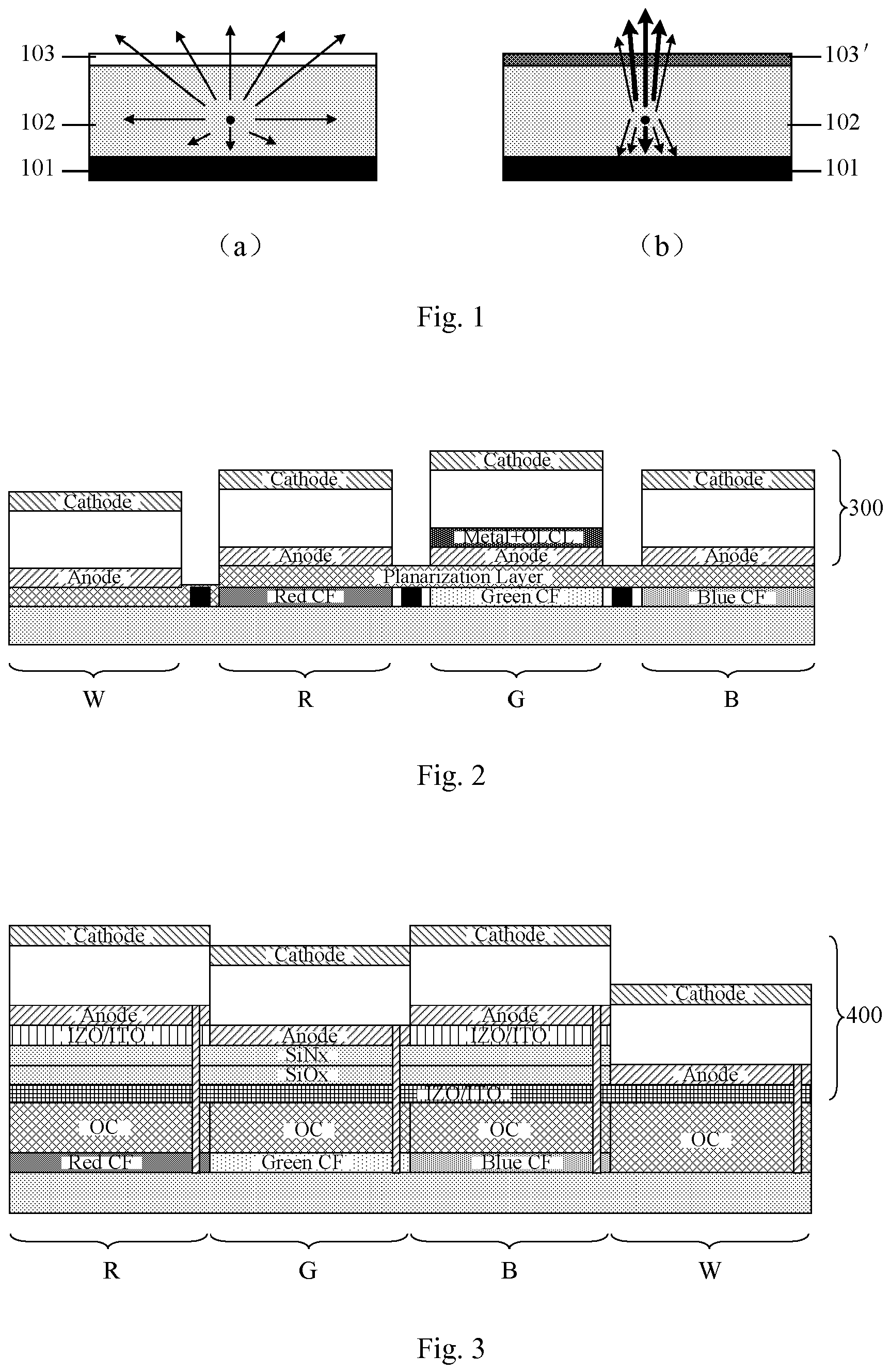
Embodiments of the present invention relate to the field of display technology, particularly to an array substrate, a method for manufacturing the same, and a display device comprising the array substrate. Organic Light-Emitting Diodes (OLED) is considered as one of the most important display technologies in the future for its advantages in simple manufacturing process, low cost, the arbitrarily adjustable color of its emitting light in region of visible light, suitable for manufacturing a large size display device and the flexible and the like. Especially the white OLED (WOLED) has a power efficiency over 60 Im/W and a lifetime more than 20,000 hours, greatly promoting development of the WOLED. As illustrated in As can be seen from Patent document Patent document Technical problem to be solved by embodiments of the present invention is how to manufacture a microcavity structure with simple manufacturing process and increase transmittance of a WOLED display device. To solve the above technical problem, the present embodiments of the present invention provide an array substrate comprising a base substrate and a plurality of pixel units disposed on the base substrate, each of the pixel units comprising:
In an embodiment of the present invention, a pixel define layer is also formed in a corresponding region of the thin film transistor structure of the pixel units and on the first electrode. In an embodiment of the present invention, the transflective layer is made of any one of silver, aluminum, molybdenum, copper, titanium, chromium and alloys thereof and has a transmittance in a range of 5%-95%. In an embodiment of the present invention, the transflective layer has a thickness between 10 Å to 200 Å. In an embodiment of the present invention, the color filters have a thickness in a range of 1000 Å to 40000 Å. In an embodiment of the present invention, the color filter is a color filter of RGB mode, RGBY mode or RGBW mode. Embodiments of the present invention also provide a method for manufacturing such an array substrate, comprising:
In an embodiment of the present invention, forming patterns of the transflective layer and the color filter in the pixel region of the pixel unit comprising:
In an embodiment of the present invention, forming the OLED in the pixel region of the pixel units comprising:
Embodiments of the present invention provide a display device comprising the array substrate mentioned above. Embodiments of the present invention increase transmittance of light by forming a microcavity structure between the transflective layer and the reflective electrode of the OLED (the cathode or the anode). And furthermore, as the color filter is formed on the transflective layer, the color filter is inside the microcavity structure for each pixel unit. As the color filters of pixel units of different colors are formed in different steps, their thickness can be easily controlled respectively. Thus, the array substrate according to embodiments of the present invention is easy to manufacture at a low cost. In order to clearly illustrate the technical solution of the embodiments of the invention, the drawings of the embodiments will be briefly described in the following; it is obvious that the described drawings are only related to some embodiments of the invention and thus are not limitative of the invention.
In order to make objects, technical details and advantages of the embodiments of the invention apparent, the technical solutions of the embodiment will be described in a clearly and fully understandable way in connection with the drawings related to the embodiments of the invention. It is obvious that the described embodiments are just a part but not all of the embodiments of the invention. Based on the described embodiments herein, those skilled in the art can obtain other embodiment(s), without any inventive work, which should be within the scope of the invention as defined in the appended claims. As illustrated in To obtain a microcavity structure, the pixel unit of the array substrate according to the present embodiment further comprises a transflective layer 8. The transflective layer 8 is located between the OLED and the passivation layer, the color filter 9 is located between the second electrode 14 of the OLED and the transflective layer 8, and color filters 9 of different colors have different thicknesses. The second electrode 14 of the OLED and the transflective layer 8 form a microcavity structure, wherein the color filter 9 is located inside the microcavity structure and between the second electrode 14 of the OLED and the transflective layer 8. Therefore, it is possible to adjust the thickness of the microcavity structure through controlling the thickness of the color filter 9; since the color filters of the pixel units of different colors are to be formed in different steps, thicknesses thereof can be easily controlled respectively, without additionally forming other layers individually for a pixel unit of a certain color in order to control its thickness. Therefore, the array substrate according to embodiments of the present invention can be easily manufactured at low cost. The thin film transistor structure, as shown in In the present embodiment, a transflective layer 8 is formed over the passivation layer 7 and a color filter 9 is formed over the transflective layer 8. The OLED is disposed over the transflective layer 8 and the color filter 9 and is formed in pixel region A through a pixel define layer (PDL). In the present embodiment, the first electrode 11 is an anode, the second electrode 14 is a cathode (or, the first electrode 11 is a cathode and the second electrode 14 is an anode) and the first electrode 11 is connected to the second drain through a via hole in the passivation layer 7. The second electrode 14 can be a reflective electrode made of a reflective material. The second electrode 14 can be coated with a reflective layer in order to form a reflective electrode. The gate (the first gate 2) of the switching thin film transistor is connected to the gate lines, the source (the first source) of the switching thin film transistor is connected to the data lines, the drain (the first drain) of the switching thin film transistor is connected to the gate (the second gate 2') of the driving thin film transistor, the source (the second source) of the driving thin film transistor is connected to a power voltage, the drain (the second drain) of the driving thin film transistor is connected to the first electrode 11 of the OLED. White light emitted by the white organic light-emitting layer 13 exits from bottom of the base substrate 1 after passing through the first electrode 11 and the underlying layers, as illustrated in To increase the spatial distance of the microcavity structure and further increase the transmittance, a resin layer 10 is formed between the color filter 9 and the anode 11, and the first electrode 11 is connected to the second drain by a via hole through the passivation 7 and the resin layer 10. In the present embodiment, the transflective layer 8 has a transmittance in a range of 5% to 95%, and is made of any one of silver, aluminium, molybdenum, copper, titanium, chromium and alloys thereof. The transflective layer 8 has a thickness in a range of 10 Å to 200 Å. The color filter 9 has a thickness in a range of 1000 Å to 40000 Å and can be a color filter of RGB mode, RGBY mode or RGBW mode. Embodiments of the present invention also provide a method of making the array substrate mentioned above, the method comprises:
Formation of the color filter 9 is completed in a plurality of processes steps (3 processes for RGB) with one process step for a color filter of one color. The pattern of the color filter 9 is formed by sequentially forming patterns of color filters of different colors. The color filters 9 is formed by: forming a color filter film of one color on the transflective layer 8 and forming a pattern of a filter for this color on the pixel region A by a patterning process. Patterns of the filters of other colors are formed sequentially in this manner, to form patterns of the color filters 9, and when patterns of the filters for each color are formed, the color filter films of each color formed have different thicknesses, so that color filters of different colors of the color filter 9 finally formed have different thicknesses. The color filters 9 finally formed have a thickness in a range of 1000 Å -40000 Å; the reason that the color filters have a wide thickness range is the color filter is provided in the microcavity structure and thus thickness of the microcavity structure can be controlled through adjusting the thickness of the color filters, so that microcavity structure in each pixel unit enhances light of the same color as that of the color filter 9. Since color filters of the pixel units of different colors are formed in different steps with their thicknesses to be controlled separately and without requiring to form additional and individual other layers for pixels of a certain color to control its thickness, therefore, the array substrate according to the present invention can be easily manufactured at a low cost. Step S3: forming an OLED in the pixel region A of the pixel unit, such that the transflective layer 8 and the color filters 9 are disposed between the OLED and the thin film transistor structure. This step comprises the following: Etching via holes in the passivation layer 7 through a patterning process, as shown in Forming a transparent conductive film, as shown in Forming an insulation film, as shown in Forming an organic light-emitting layer 13 and a second electrode 14 of the OLED, so that the OLED is formed. The array substrate finally formed is shown in Embodiments of the present invention also provide a display device comprising the above said array substrate. The display device may be any product or component having a display function, such as an electronic paper, an OLED panel, and OLED display, an OLED TV, a digital photo frame, a mobile, a laptop and the like. The foregoing are merely exemplary embodiments of the invention, but are not used to limit the protection scope of the invention. The protection scope of the invention shall be defined by the attached claims. An array substrate comprising a base substrate (1) and a plurality of pixel units disposed on the base substrate (1), each of the pixel units comprising:
a thin film transistor structure on the base substrate; and an OLED driven by the thin film transistor structure, the OLED disposed in the pixel region of the pixel units, the OLED sequentially including a first electrode (11) which is transparent, an organic light-emitting layer (13) and a second electrode (14) in a direction away from the base substrate (1), the second electrode (14) used for reflecting lights; a transflective layer (8) disposed between the OLED and the thin film transistor structure; a color filter (9) disposed between the second electrode (14) of the OLED and the transflective layer (8); wherein the second electrode (14) of the OLED and the transflective layer (8) constitute a microcavity structure; the thin film transistor structure comprises a first gate (2) and a second gate (2') on the base substrate (1), a gate insulation layer (3) over the first gate (2) and the second gate (2'), a first active layer (4) and a second active layer (4') on the gate insulation layer (3), a first source and a first drain (6) on the first active layer (4), a second source and a second drain (6') on the second active layer (4'), the first drain (6) being connected to the second gate (2'), the first gate (2), the gate insulation layer (3), the first active layer (4), the first source and the first drain (6) constituting a switching thin film transistor, the second gate (2'), the gate insulation layer (3), the second active layer (4'), the second source and the second drain (6') constituting a driving thin film transistor; the second drain (6') of the driving thin film transistor and the first electrode (11) of the OLED are electrically connected, a passivation layer (7) is disposed on the thin film transistor structure; the OLED is disposed over the passivation layer (7), the transflective layer (8) is disposed over the passivation layer (7), the color filter (9) is disposed over the transflective layer (8), the color filter (9) of different colors has different thickness, both the transflective layer (8) and the color filter (9) are disposed in the pixel region of the pixel units, and the first electrode (11) of the OLED is located above the color filter, the array substrate being characterized in that, the array substrate comprises a resin layer (10) disposed between the color filter (9) and the first electrode (11), the first electrode (11) being connected to the second drain (6') by via holes through the resin layer (10) and the passivation layer (7). The array substrate according to claim 1, further comprising a pixel define layer (12) disposed in a region corresponding to the thin film transistor structure of the pixel units and above the first electrode (11). The array substrate according to any one of claims 1 to 2, wherein the transflective layer (8) is made of any one of silver, aluminum, molybdenum, copper, titanium, chromium and alloys thereof and has a transmittance in a range of 5% to 95%. The array substrate according to any one of claims 1 to 3, wherein the transflective layer (8) has a thickness in a range of 10 Å to 200 Å. The array substrate according to any one of claims 1 to 4, wherein the color filter (9) has a thickness in a range of 1000 Å to 40000 Å. The array substrate according to any one of claims 1 to 5, wherein the color filter (9) is a color filter of RGB mode, RGBY mode or RGBW mode. A method for manufacturing the array substrate of claim 1, the method comprising following steps:
forming patterns of a thin film transistor structure and a passivation layer (7) on a base substrate (1) to define a plurality of pixel units on the base substrate (1); forming patterns of the transflective layer (8) and the color filter (9) in a pixel region of the pixel units such that the color filter (9) is disposed above the transflective layer (8); the color filter (9) of different color has different thickness; and forming an OLED in the pixel region of the pixel units so that the transflective layer (8) and the color filter (9) are disposed between the OLED and the thin film transistor structure; the method being characterized in that the method further comprises forming a resin layer (10) after patterning the transflective layer (8) and the color filter (9) and before forming the OLED The method according to claim 7, wherein forming patterns of the transflective layer (8) and the color filter (9) in the pixel region of the pixel units comprises:
forming a transflective film on the passivation layer (7) and forming patterns of the transflective layer (8) in the pixel region through a patterning process; forming a color filter film of one color on the base substrate formed with the transflective layer, forming a pattern of the color filter (9) in the pixel region through a patterning process and forming patterns of color filters (9) of other color sequentially in this manner so that patterns of the color filters (9) are formed. The method according to claim 7, wherein forming the OLED in the pixel region of the pixel units comprises:
forming via holes through the resin layer (10) and the passivation layer (7) by a patterning process; forming a transparent conductive film, and forming patterns of the first electrode (11) of the OLED through a patterning process so that the first electrode (11) is connected to the thin film transistor structure (6') through via holes; forming an insulation film, and patterning patterns of the pixel define layer (12) through a patterning process so that position of the OLED to be formed is defined in the pixel region; forming an organic light emitting layer (13); and forming a second electrode (14) of the OLED and thus forming the OLED, the second electrode (14) used for reflecting light. A display device including the array substrate according to claim 1.TECHNICAL FIELD
BACKGROUND
SUMMARY
BRIEF DESCRIPTION OF THE DRAWINGS
DETAILED DESCRIPTION
A transflective film is formed on the passivation layer 7. The transflective film is made of any one of silver, aluminum, molybdenum, copper, titanium, chromium and alloys thereof and has a thickness in a range of 10 Å-200 Å and a transmittance in a range of 5%-95%. A pattern of the transflective layer 8 is formed in the pixel region A through a patterning process after the transflective film is formed.


CPC - классификация
HH1H10H10KH10K5H10K50H10K50/H10K50/8H10K50/85H10K50/852H10K50/856H10K59H10K59/H10K59/1H10K59/12H10K59/120H10K59/1201H10K59/124H10K59/13H10K59/131H10K59/3H10K59/38H10K59/8H10K59/87H10K59/876H10K59/878H10K7H10K71H10K71/H10K71/0H10K71/00IPC - классификация
HH0H01H01LH01L2H01L27H01L27/H01L27/3H01L27/32H01L5H01L51H01L51/H01L51/5H01L51/52Цитирование НПИ
JP-A- 2010 010 020JP-A- 2010 287 543
KR-A- 20080 047 782