METHOD FOR MANUFACTURING THIN FILM WITH THREE-DIMENSIONAL NANOPOROUS STRUCTURE BY USING BAFFLE AND THIN FILM WITH THREE-DIMENSIOANAL NANOPOROUS STRUCTURE MANUFACTURED BY SAME
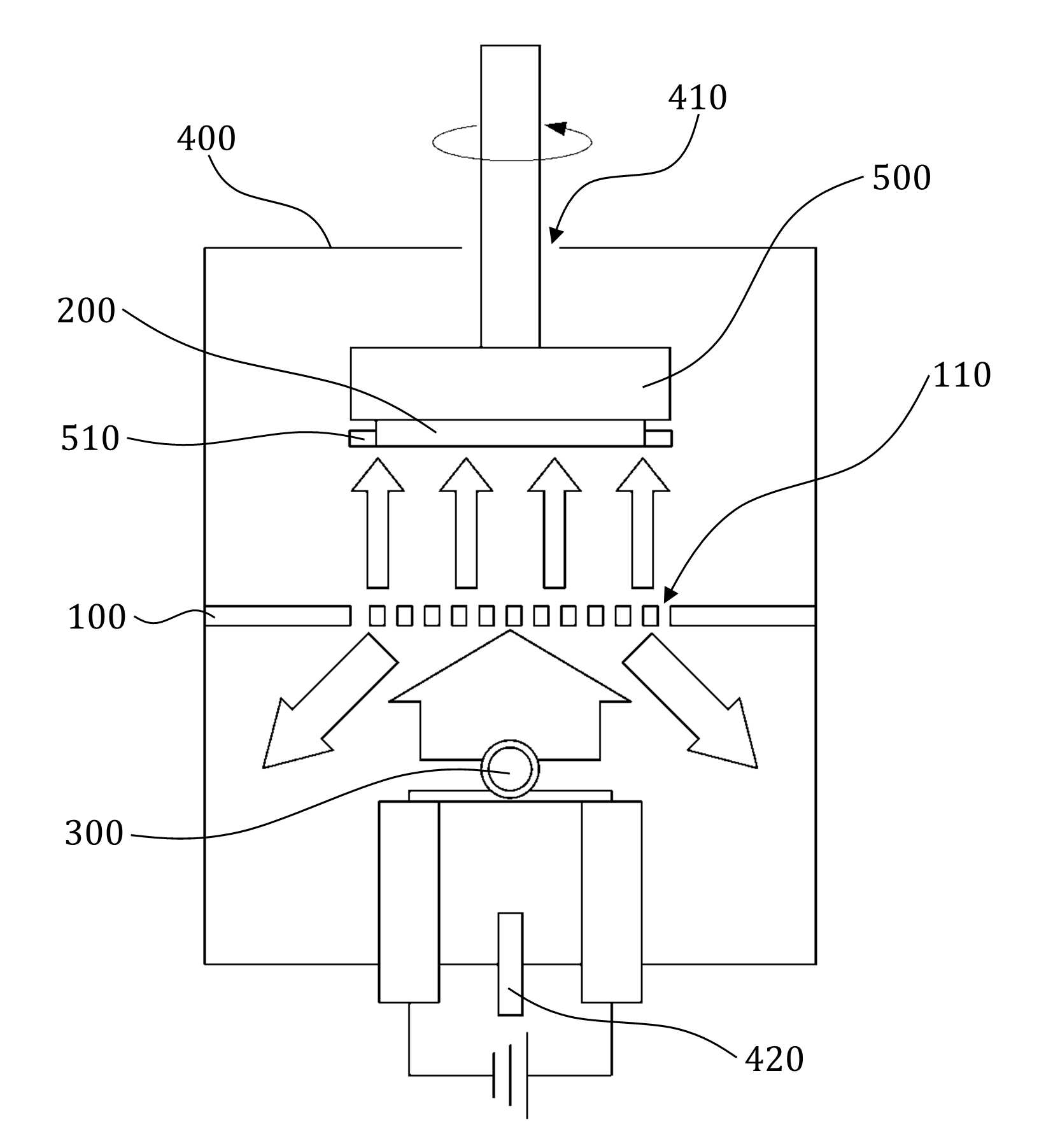
The invention relates to a 3 dimensional structure and manufacturing method of thin nanoporous using baffle, baffle (baffle) performance is provided apparatus and method for using the lamp various material on the substrate of the method for manufacturing thin film nanoporous 3 dimensional structure are disclosed. Nanoporous materials at the nano level monosized pores and porosity (porosity) is 0. 2 - 0. 95 having the pores of the powder, thin film, thick film material and porous material bulk form of big. IUPAC criteria of pore sizes equal to or less than 2 nm (micropore) along microporous, mesoporous (mesoporous) range of 2 - 50 nm, 50 nm or more (Macropore) etc. and divided into large pores. The workpiece is generally nano pore size 0. 4 - 100 nm range to about dropped on the porous material. Recent applications utilizing to acquire the nanoporous material separation and adsorption reaction substances that is receiving only molecular recognition function field environment with a silica planar lightwave, biochemical reaction detecting chemical and biosensor field, mesoporous and fully utilize the high specific surface area capable of supercapacitor and portable fuel cell applications, low dielectric thin film etc. for insulating material for electronic/information. By a conventional method for producing such porous membrane, pore-forming a metal ligand alkyl groups and solvent by vaporization of the brush gel law, unique particles 5.0 particles forming coating pores-molding space, the thin film is template (template) through the template method to remove repulsion SiB4 etc.. A compensation registration Internet route 10 - 1000476 call (conveys: macro size pupil and a macroparticle size pupil mixing pupil structure of 3 dimensional porous carbon nanotube films, referred to as prior art 1 etched below.) in, oxynitride processing carbon nanotubes, carbon nanotube powder uniformly dispersed solvent and, dispersed solution by adding anionic surfactant precursor making a solution, precursor solution is sprayed onto the substrate electrostatically using EASP (Electrostatic Aerosol Spray Pyrolysis) formed carbon nanotube thin film, carbon nanotube films removed from the anionic surfactant solution having 3 dimensional macro size pupil and pupil size mixing pupil structure described porous fabricating carbon nanotube thin film method. The prior art is 1, wet process using porous thin film is formed by heat treatment, the initial surface area wider but, for vaporizing the solvent in the drying and sintering the first reduced surface to produce a pore that does lowering degree 1. Also, the prior art 1 is, carbon nanotube powder precursor solution comprising electrically charged anionic sprayed onto the porous forming a thin film on the substrate, a variety of parts formed of paper or plastic or ceramic material cannot be first does a porous thin film 2. And, the prior art is 1, a quantity of chemical waste emits, as an ion implantation mask high blade 3 makes a first mass does. The present invention accomplish in a border or more pipeline not limited or resonance, not in yet another technique are referred from the substrate below the first consultation with knowledge of this invention is to be able to clearly is a device are disclosed. In order to achieve the the swing, the one embodiment of the present invention, (i) substrate to immobilize and, for evaporating the substrate won (heat source) is desired locations is then heat cutting having function of baffles (baffle); (ii) the deposition chamber so as to form a step further; (iii) the deposition chamber vacuum state is initially the process gas injection flow forming process pressure; (iv) the temperature of the substrates according to setting a substrate temperature below 50 °C; (v) thermal deposition process won the vaporized deposition material container forming a deposition material (heat source) and the increasing temperature of the (v) (vi) generated in the and by the deposition particle is deposited on a substrate, the (i) the step of the baffle (baffle), won the vaporized (heat source) of heat generated by radiation, convection and conduction with a function to inhibit dimensional structure and manufacturing method of thin baffles that characterized using nanoporous 99900000949 99 efficacy. In embodiments of the present invention, the (i) step baffle, migration of particles it became other hole (hole) can be formed for the deposition. In embodiments of the present invention, the hole (hole) is, be a won or polygonal shape. In embodiments of the present invention, the step (i) baffle, one or more operated at less than 1 can be formed on the semiconductor substrate 3. In embodiments of the present invention, the step (i) has an thickness, 0. 2 or more 30 millimeter (mm) can be below. In embodiments of the present invention, the step (i) baffle metal, alloy and ceramic material selected from the group consisting of one or more material can be formed. In embodiments of the present invention, the iron (Fe) baffle step (i), titanium (Ti), molybdenum (Mo), cobalt (Co), nickel (Ni), tungsten (W), beryllium (Be), lead (Pb), tin (Sn), silicon (Si), chromium (Cr), zinc (Zn), copper (Cu) and aluminum (Al) can be at least one metal selected from the group consisting. In embodiments of the present invention, the step (i) baffle alumina, silicon nitride, silicon carbide and zirconia ceramic material can be at least one selected from the group consisting. In embodiments of the present invention, the step (i) a substrate of paper, synthetic resin, ceramic material, glass, silicon, metal and at least one material selected from the group consisting can be formed. In embodiments of the present invention, baffle between the substrate and the distance between the, 0. 01 or more 45 centimeter (cm) can be below. In embodiments of the present invention, the distance between the substrate and evaporation won, 100 centimeter (cm) can be below 3 or more. In embodiments of the present invention, the (iv) step, cooling said substrate secured seal can be carried out. In embodiments of the present invention, the deposition chamber, the deposition of the vaporized from a top surface of the flow won the deposition chamber with a top surface of the data line port is the deposition chamber can be. In embodiments of the present invention, the deposition chamber, the deposition particles flow from the vaporized won on the side of the deposition chamber port is on the side of the deposition chamber to a predetermined location with the data line can be. In embodiments of the present invention, the step (iii) initial process pressure is, 0. 01 Torr or more 30 Torr or less disclosed. In embodiments of the present invention, the deposited particles speed 0. 01 to 10 micrometers (micro m/min)/minutes implementation being. In embodiments of the present invention, the deposited particles, gold (Au), is (Ag), palladium (Pd), aluminum (Al), copper (Cu), chromium (Cr), iron (Fe), magnesium (Mg), manganese (Mn), nickel (Ni), titanium (Ti), zinc (Zn), lead (Pb), vanadium (V), cobalt (Co), er (Er), calcium (Ca), holmium (Ho), samarium (Sm), scandium (Sc), terbium (Tb), molybdenum (Mo) and platinum (Pt) can be at least one metal selected from the group consisting. In embodiments of the present invention, the (iii) steps gas, and argon as inert gas (Ar), nitrogen (N2 ), Helium (He), neon (Ne), krypton (Kr), xenon (Xe), radon (Rn) can be at least one selected gas. In embodiments of the present invention, the deposited particles, tin (Sn), nickel (Ni), copper (Cu), titanium (Ti), vanadium (V), chromium (Cr), manganese (Mn), iron (Fe), cobalt (Co), zinc (Zn), molybdenum (Mo), tungsten (W), the (Ag), gold (Au), platinum (Pt), iridium (Ir), ruthenium (Ru), lithium (Li), aluminum (Al), antimony (Sb), bismuth (Bi), magnesium (Mg), silicon (Si), indium (In), lead (Pb) and palladium (Pd) composed of oxide of at least one metal oxide selected from the group consisting can be. In embodiments of the present invention, the metal oxide thin film is formed nanoporous 3 dimensional structure, the evaporation source material tungsten (W), molybdenum (Mo) and tantalum (Ta) can be selected from the group consisting of material. In embodiments of the present invention, the (iii) in the second process gas can, and argon as inert gas (Ar), nitrogen (N2 ), Helium (He), neon (Ne), krypton (Kr), xenon (Xe) and radon (Rn) selected from the group consisting at least one gas and oxygen (02 ) Mixture with, the oxygen (02 ) Is the metal oxide component can ensure stability of control and performing the function of oxidation state. In embodiments of the present invention, the generation of particles deposition at step (v), can be ten evaporation laws by sputtering or evaporation. In embodiments of the present invention, the step (vi), the deposition chamber process gas species, process pressure, the temperature of the substrates, between the substrate and the deposition of one or more evaporation won and distance between heating temperature change over time and varying the amount of energy to the deposition particles, as a consequence the nanoporous 3 dimensional structure of uniform quality can be formed inward direction density beam expander in thin film thickness. In embodiments of the present invention, the processing pressure (vi) step performed in time (gradually) progressively increasing, the nanoporous 3 dimensional structure within thin film, thereby forming the thin film thickness relative density can progressively decreases or increases. In embodiments of the present invention, the pressure in the second process (vi) (discretely) over time discretely increasing, the nanoporous 3 dimensional structure within the thin film, the thin film thickness decreases or increases thereby forming an discretely relative density can have a multilayer structure be. In order to achieve the the swing, the one embodiment of the present invention, a method for producing thin film nanoporous 3 dimensional structure produced by using baffles, specific surface area (specific surface area) value is 0. 1 to 600 m2 In nanoporous 3 dimensional structure characterized/g thin film substrate. In embodiments of the present invention, the dimensional structure thin film density for the empty (bulk contrast) is nanoporous 3 0. 01 to implementation being 90%. In embodiments of the present invention, the dimensional structure thin film is nanoporous 3, diameter 1. 0 to 100 nanometer (nm) in the mesopores (mesopore) can be. In embodiments of the present invention, the dimensional structure thin film is nanoporous 3, diameter 1. 0 to 100 nanometer (nm) in mesopores (mesopore) on diameter 0. 5 micrometers (micro m) or more can be simultaneously having macropores (macropore) network. In order to achieve the the swing, the one embodiment of the present invention, gas sensor, biosensor, battery, capacitor, fuel cell, solar cell, chemical catalyst, is connected to the electrode (electrode) 3 dimensional structure in nanoporous antimicrobial filter, the porous surface of electrodes with, nanoporous 3 dimensional structure of the present invention the 3 dimensional structure electrode thin film nanoporous characterized efficacy. In order to achieve the the swing, the one embodiment of the present invention, vacuum and collapsed positions having a deposition chamber; applying heat energy supply located at the lower end of the deposition chamber deposition material evaporation won; fixed and cooled cooling substrate located on top of the deposition chamber; the evaporation source which is interposed between the substrate, deposition particles pass through a plurality of holes is located in a top surface of the baffle and the deposition chamber, the deposition particles flow from the vaporized won the deposition chamber to be formed vent valve which in a blade, the deposition chamber process gas species, process pressure, the temperature of the substrates, between the substrate and the deposition of one or more evaporation won and distance between heating temperature change over time to vary the size of the deposited energy particles characterized nanoporous 3 dimensional structure using baffles that separated from each other. In embodiments of the present invention, the baffle, one or more operated at less than 1 can be formed on the semiconductor substrate 3. In embodiments of the present invention, the baffle, the evaporation source can be installed on one plurality between said substrates. The invention relates to a, dry thin film forming method by amount, not two separate drying and sintering process also ensure the durability of the pores can be nanostructured and nanoporous 3 dimensional structure, a substrate having a porous thin film adhesion foreign matter along side reaction (specific surface area) can be 1 to improve a first effect. The invention also relates to, is in a charged substrate, low temperature surface of a substrate thermal deposition process can produce a nanoporous 3 dimensional structure, such as a sheet of paper or plastic or ceramic material various material deposition material 2 can be selected as the first effect. Also, the present invention relates, in particular the lamp material determines whether the PCB, when particles of the deposition material thickness which can be uniformly distributed on the surface substrate, depositing material deposition rate improving effect that 3 first. And, the invention relates to, minimise chemical waste, mixed porous thin film deposition process is simple keeping 4 it is possible to first effect. The effect of the present invention has the effect confined within, or the claims of the present invention deduced from a description of all possible for reducing the should is understood to. Figure 1 shows a part of the nanoporous 3 dimensional structure in one embodiment are also regards chamber are disclosed. Figure 2 shows a nanoporous 3 dimensional structure in one embodiment are also part of the other chamber regards are disclosed. Figure 3 shows a also, in one embodiment of the present invention features a plane baffle (baffle) are disclosed. Figure 4 shows a baffle (baffle) also if there is not, in one embodiment of the present invention dimensional structure thin film deposition chamber for the flow of particles deposited in a nanoporous 3 mimetic are disclosed. Figure 5 shows a baffle (baffle) also if, in one embodiment of the present invention dimensional structure thin film deposition chamber for the flow of particles deposited in a nanoporous 3 mimetic are disclosed. Figure 6 shows a thin film nanoporous 3 dimensional structure are also thin film in the thickness direction so as to have a mimetic representing embodiments for gradual density uniform quality are disclosed. Figure 7 shows a thin film nanoporous 3 dimensional structure are also thin film in the thickness direction so as to have uniform quality gradual density representing other embodiments a mimetic are disclosed. Figure 8 shows a nanoporous 3 dimensional structure are also discrete density thin film in the thickness direction so as to have uniform quality thin film mimetic representing embodiments are disclosed. Figure 9 shows a nanoporous 3 dimensional structure are also discrete thin film in the thickness direction so as to have uniform quality thin film density is a mimetic representing other embodiments. Figure 10 shows a silicon wafer (Si wafer) on 23 °C therefore cooling through embodiments of the present invention in 3 dimensional structure for SEM Image thin film nanoporous are formed on the substrate are disclosed. Figure 11 shows a coolant through the silicon wafer (Si wafer) are also embodiments for 3 °C on nanoporous 3 dimensional structure formed over a substrate in thin film for SEM Image are disclosed. Figure 12 through silicon wafer (Si wafer) are formed on the substrate of the present invention embodiments for copper thin film nanoporous 3 dimensional structure Image photographing are disclosed. Figure 13 through silicon wafer (Si wafer) are formed on the substrate of the present invention embodiments for dimensional structure for copper thin film nanoporous 3 SEM Image are disclosed. Figure 14 0 through embodiments of the present invention. 1Torr process under pressure, copper thin film on the glass substrate nanoporous 3 dimensional structure Image photographing are disclosed. Figure 15 0 through embodiments of the present invention. 2Torr process under pressure, copper thin film on the glass substrate nanoporous 3 dimensional structure Image photographing are disclosed. Figure 16 0 through embodiments of the present invention. 5Torr process under pressure, copper thin film on the glass substrate nanoporous 3 dimensional structure Image photographing are disclosed. Figure 17 the 1Torr process under pressure through embodiments of the present invention, copper thin film on the glass substrate nanoporous 3 dimensional structure Image photographing are disclosed. In embodiments of the present invention through a process pressure of 5Torr Figure 18, Image photographing copper thin film on the glass substrate nanoporous 3 dimensional structure are disclosed. Figure 19 paper are formed on the substrate of the present invention embodiments for copper thin film nanoporous 3 dimensional structure through Image photographing are disclosed. Figure 20 through polyimide film (PI film) are formed on the substrate of the present invention embodiments for copper thin film nanoporous 3 dimensional structure Image photographing are disclosed. Embodiments of the present invention Figure 21 through alumina (Al2 O3 ) Are formed on the substrate Image photographing copper thin nanoporous 3 dimensional structure are disclosed. In embodiments of the present invention through a process pressure of Figure 22 1Torr baffle 3 dimensional structure without the use of palladium (Pd) thin film nanoporous deposited GDL (Gas Diffusion Layer) photographing Image are disclosed. Figure 23 through use of the present invention embodiments for 1Torr process under pressure baffle (Gas Diffusion Layer) palladium (Pd) thin film nanoporous 3 dimensional structure deposited on the GDL is supplied photographing are disclosed. Figure 24 through use of the present invention embodiments for 5Torr process under pressure baffle (Gas Diffusion Layer) palladium (Pd) thin film nanoporous 3 dimensional structure deposited on the GDL photographing Image are disclosed. Embodiments of the present invention along Figure 25 repeat the process of palladium (Pd) when GDL (Gas Diffusion Layer) nanoporous 3 dimensional structure deposited thin film photographing Image are disclosed. Embodiments of the present invention repeat the process of Figure 26 along 3 dimensional structure palladium (Pd) when GDL (Gas Diffusion Layer) for SEM Image nanoporous deposited thin film are disclosed. Is less than the judged HTML page which utilizes the present invention to explain less than 1000. However the present invention can be embodied in the form of several different, not the confined within the embodiments taught herein. For clarifying the present invention in the seller account for dispensed when the portion is described that is independent, like part subjected to a similar drawing code is configured to receive the area to herein. The entire herein, any portion to other assistant "(connection, contact, coupled) connected" when, this "connected directly" as well as when, the other interposed therebetween intermediate comprises a unit when "indirectly connected". Also any portion of any components that "comprising" when, without other components particularly the opposite substrate excepting the other components but further switched to each other. Term used herein is used only to account for certain embodiments, the present invention intending to be limited is endured. It is apparent that a single representation of the differently in order not providing language translators, comprising plurality of representation. Herein, the term "comprising disclosed" or "has disclosed" a description of features, numbers, steps, operations, elements, components or specify a combination not present included, another aspect of one or more moveable number, step, operation, component, component or a combination of these items will advance the possibility or not should the presence of or additionally. To the rotating velocity of the rotor of the present invention embodiments for detailed the on-sensors other. Figure 1 shows a nanoporous 3 dimensional structure in one embodiment are also thin film deposition chamber (400) for schematic and, Figure 2 in one embodiment of the present invention thin film deposition chamber of a nanoporous 3 dimensional structure (400) from other schematic are disclosed. Figure 3 shows a baffle (baffle) according to embodiments of the present invention and therefore which features high flatness, baffle (baffle) Figure 4 (100) if there is not, in one embodiment of the present invention thin film deposition chamber of a nanoporous 3 dimensional structure (400) disposed inside the particles which flow type, Figure 5, baffle (baffle) (100) if, in one embodiment of the present invention thin film deposition chamber of a nanoporous 3 dimensional structure (400) disposed inside a mimetic for the flow of particles are disclosed. (Also 1 and of Figure 2 arrows of thermal energy flow representing, representing other. 4 of Figure 5 and also flow of deposition particles arrows) Also with reference to the 1 to 5 also, a kind of baffle (baffle) (100) using nanoporous 3 dimensional structure and method of preparation thereof for, each less than processes detailed the on-sensors other. (Also 1 and in Figure 2 hole (110) (hole) and outlet (410) is understanding for facilitating significantly presented and, in Figure 1 is an exhaust port (410) is deposited chamber (400) end portion of the braided with one another, in Figure 2 is an exhaust port (410) is deposited chamber (400) are formed on a top been.) First, deposition chamber (400) substrate (200) fixing and, substrate (200) for evaporating a won (heat source) (300) is heat cutting desired locations having function of baffles (baffle) (100) can be installed. The, baffle (baffle) (100) is, won evaporation (heat source) (300) of heat generated by radiation, convection and conduction can be with that function. Wherein, baffle (100) for migration of particles deposited it became other hole (hole) (110) can be formed. At this time, hole (hole) (110) can be won or polygonal shape of the. Baffle (100) is, evaporation of deposition material when a semiconductor substrate on which a thermal energy is supplied by suppressing effectively transmitted through convection or conduction or radiation, substrate (200) can be a low temperature of, substrate (200) can be minimize temperature increases occur in the surface. The tubes (100) is, formed in particles produced by deposition material deposited on the substrate (200) be deposited to plurality of perforations (hole) (110) can be formed. it became other hole (hole) at constant intervals (110) through the substrate (200) migration to the surface of deposition particles, substrate (200) while uniformly distributed on the surface of constant thickness and forms can be deposited. Hole (110) is, may be won or polygonal shape, positions for enhanced uniformity of won can be preferably. The entire hole (110) the area of the, baffle (100) of the whole area, 0. Be a ratio less than 1% 70% or more. The entire hole (110) area of the baffle (100) the whole area 0. Is below 1%, the deposition efficiency are lower keep down and restrict the deposited particles to pass through, the entire hole (110) area of the baffle (100) is greater than the whole area 70%, baffle (100) can be thermal inhibiting effect. Hole (110) is, constant size can be formed, baffle (100) in a central portion of the inner space formed in the nozzle is so size changes gradually holds disapproval. Also, hole (110) is, constant and may be formed at regular intervals, so that the uniformity of deposition variation of different intervals along and disposed so as to be formed may be filled. Baffle (100) is, at least one operated at less than 1 can be formed on the semiconductor substrate 3. Baffle (100) has a thickness of, 0. 2 or more 30 millimeter (mm) can be below. Baffle (100) has a thickness of, hole (110) depending on the size of or, in efficiency 0. 2 millimeter (mm) or more preferably less than 30 millimeters (mm). Baffle (100) having a thickness of 0. 2 millimeter (mm) is below, baffle (100) the thermal effect and baffle (100) and may cause a decrease in the durability of, baffle (100) 30 millimeter (mm) thickness of greater than surface, is considerably limited amount can be deposited particles to pass through. The thickness in a range of, baffle (100) is operated at less than 3 one or more can be formed on the semiconductor substrate 1, but accepts an inhibitory effect on several layers formed in the material thermal high efficiency high, but the other layer is formed an inhibitory effect on thermal energy 670 it is that expense material, considering cost and efficiency can be selectively selecting material. But, baffle (100) the plurality of layer if formed each hole (110) and the inner surfaces of said divided variety, each divided area between the deposited deposition of nano-size particles, hole (110) lost particles deposited in the deposition, hole (110) can be disturb a flow of particles through the deposition. This phenomenon is baffle (100) is formed on the semiconductor substrate so that the at least one 4 when significant, baffle (100) is preferably formed on the semiconductor substrate can be operated at less than 3. Baffle (100) metal, alloy and ceramic material selected from the group consisting of one or more material can be formed. Baffle (100) while inhibiting heat energy at an elevated temperature, low thermal conductivity and can be made of material having heat resistance. Baffle (100) iron (Fe), titanium (Ti), molybdenum (Mo), cobalt (Co), nickel (Ni), tungsten (W), beryllium (Be), lead (Pb), tin (Sn), silicon (Si), chromium (Cr), zinc (Zn), copper (Cu), aluminum (Al) made of single metal and their alloy, or carbon steel, stainless steel, bronze, brass, beryllium - copper alloy, copper - aluminum alloy, cubic boron nitride (BN), aluminum oxide (Al2 O3 ) Can be made of a high-refractive-alloy or oxide. Also, baffle (100) alumina, silicon nitride, silicon carbide, zirconia ceramic material such as their can be made using ceramic composite. Substrate (200) paper, synthetic resin, ceramic material, glass, silicon, metal and at least one material selected from the group consisting can be formed. Baffle (100) is less than 50 °C effectively transfer of thermal energy while suppressing low temperature substrate (200) accessories to the deposited particles distributed evenly thickness, substrate (200) can be formed from a variety of materials with low thermal conductivity. Substrate (200) polyimide (PI), polyethylene naphthalate (PEN), polyethylene terephthalate (PET), polyurethane, Nafion can be formed of synthetic resin material. Also, substrate (200) alumina, silicon nitride, silicon carbide, zirconia ceramic material such as their can be using ceramic composite material. And, paper, glass, as well as wood front, GDL material substrate produced a variety of fuel cell (Gas Diffusion Layer) (200) can be deposited to. Substrate (200) and an air baffle (100) and the distance between the, 0. 01 or more 45 centimeter (cm) can be below. Substrate (200) and an air baffle (100) distance between, 0. 01 centimeter (cm) is below, substrate (200) and an air baffle (100) flag can be deposition process control is dropped onto the substrate can be, 45 centimeter (cm) is greater than, baffle (100) substrate passes through a deposition material (200) can be taken out of the chamber will not reach the vapor deposition can be lowered. In this case, substrate (200) for evaporating a won (300) between a plurality of baffle (100) is installed in a deposition process can be control. Substrate (200) for evaporating a won (300) and the distance between the, 100 centimeter (cm) can be below 3 or more. Substrate (200) for evaporating a won (300) distance between, 3 centimeter (cm) is below, substrate (200) of a temperature control unit becoming a deposition efficiency are considerably reduced and, due to the high temperature of nanoporous 3 dimensional structure portions can be difficult, 100 centimeters (cm) is greater than, deposition efficiency are reduced levels of deposition thereof can not required. Second, deposition chamber (400) further can be made. Evacuation of process can be suitably performed using equipment and, need not necessarily form a complete vacuum but not, especially metal porous thin film to be formed in order to prevent oxidation of metal when 10-5 Ensure a certain level or more initial Torr can be preferred. Third, vacuum deposition chamber (400) initial process pressure process gas into the process gas can. Wherein, the pressure early, 0. 01 Torr or more 30 Torr or less disclosed. 0 initial process pressure. 01 Torr is below, dense thin film is formed on the first thin film is formed pores (pore) there can be, if greater than 30 Torr, a large-area substrate (200) can be inspected to determine a uniformity within a and particle size. 30 Torr under the process pressure greater than deposition are electrically connected (200) can undergo collision too much until reaching's oldest. Process gas can, and argon as inert gas (Ar), nitrogen (N2 ), Helium (He), neon (Ne), krypton (Kr), xenon (Xe), radon (Rn) can be at least one selected gas. However, if not limited to gas does not react with the deposition particle. Particularly when the porous membrane to be formed oxide material, shape in addition to the oxidation state of inert gas for oxygen can be further used. The, process gas can, and argon as inert gas (Ar), nitrogen (N2 ), Helium (He), neon (Ne), krypton (Kr), xenon (Xe) and radon (Rn) selected from the group consisting at least one gas and oxygen (02 ) Mixture with, oxygen (02 ) Performing the function of the metal oxide component can ensure stability of control and oxidation state. Fourth, substrate (200) can be set below temperature of 50 °C. The, substrate (200) cooling unit (500) can be tightly secured. Substrate (200) portion of nanoporous 3 dimensional structure in the substrate (200) to maintain a certain temperature of the need to flow tides. The invention relates to a (200) -196 °C temperature of (liquid nitrogen vaporization point) or more can be maintaining isothermal temperature below 80 °C. Substrate (200) disposed radially -196 temperature than when, with the use of helium or liquid received from the separate cooler to be used circular metal plate, substrate (200) when the temperature too high, thereby making it possible to open one transfer energy deposited material reduced in the pores, which increases in size particles, porous nanostructures simultaneously applied too dense thin film is formed as long as disclosed. The isothermal maintained below 50 preferably also can be recommended. Also, substrate (200) on, locally significantly if any temperature difference, substrate (200) of the nonuniformity of porous 3 dimensional nanostructures can occur is local, it inevitably temperature variation even on process management 5 degrees and minus positive error, more preferably plus minus 1 degrees can be managed. Substrate (200) is kept constant in order to make temperature, substrate (200) cooling unit (500) can be every direction. Cooling section (500) includes a substrate by cooling water input and egress (200) and has cooled, substrate (200) can be flow uniform temperature thereby allowing. General deposition chamber (400) engage with coolant (Cooling chuck) (510) is provided on the but, the lamp parts formed (200) engage with cooling (Cooling chuck) (510) a rear only, substrate (200) and cooling (Cooling chuck) engage (510) only a portion of the contact portion and the periphery thereof be performed thermally conducting cooling can be a problem. The instant deposition chamber (400) engage in cooling (Cooling chuck) (510) with cooling (500) the lamp having parts formed (200) for cooling efficiency can be increased. (Cooling chuck) engage with cooling (510) fixed to the substrate (200) while rotating the substrate (200) can be a surface is deposited. Cooling engage (510) has a good thermal conductivity can be metal or ceramic material. Embodiment of the present invention in which a cold part (500) that is cooled by cooling water input and egress is described but, not limited to composite, such as refrigeration cycle cooler can be also be used. Fifth, thermal deposition process contained in deposition material evaporation won (heat source) (300) forming a deposition temperature control can. The, deposition particles, gold (Au), is (Ag), palladium (Pd), aluminum (Al), copper (Cu), chromium (Cr), iron (Fe), magnesium (Mg), manganese (Mn), nickel (Ni), titanium (Ti), zinc (Zn), lead (Pb), vanadium (V), cobalt (Co), er (Er), calcium (Ca), holmium (Ho), samarium (Sm), scandium (Sc), terbium (Tb), molybdenum (Mo) and platinum (Pt) can be at least one metal selected from the group consisting. And, deposition particles, tin (Sn), nickel (Ni), copper (Cu), titanium (Ti), vanadium (V), chromium (Cr), manganese (Mn), iron (Fe), cobalt (Co), zinc (Zn), molybdenum (Mo), tungsten (W), the (Ag), gold (Au), platinum (Pt), iridium (Ir), ruthenium (Ru), lithium (Li), aluminum (Al), antimony (Sb), bismuth (Bi), magnesium (Mg), silicon (Si), indium (In), lead (Pb) and palladium (Pd) composed of oxide of at least one metal oxide selected from the group consisting can be. Also, deposition particles are alumina, silicon nitride, silicon carbide, zirconia ceramic material such as using their be a ceramic composite material. Generation of deposition particles, can be ten evaporation laws by sputtering or evaporation. Especially when ten evaporation laws, heater container include crucible, coil by using a heater coil type heater, spiral coil using a spiral-type heater, etc. can be boat type heater, the heater container is made out of tungsten (W), molybdenum (Mo) and tantalum (Ta) either be a selected. In particular using boat coated with ceramics of alumina can be needed, the calcined ceramic can be formed. Nanoporous 3 dimensional structure thin film is formed of a metallic oxide, evaporation won (300) material of tungsten (W), molybdenum (Mo) and tantalum (Ta) can be selected from the group consisting of material. Evaporation won (300) a material processed (W), molybdenum (Mo) or tantalum (Ta) or the like, low vapor pressure so that oil flows by the deposition does not. However, if metal oxide deposition, tungsten (W) metal oxide is included as having an oxygen content, such as molybdenum (Mo) or tantalum (Ta) evaporation won (300) material is response, evaporation won (300) formed oxide material, such evaporation won (300) is deposited oxide material deposition of material with particles that can be deposited thin film nanoporous 3 dimensional structure of the present invention. An associate, fifth step deposition particles generated in the substrate (200) can be deposited on. The, deposition chamber (400) is, the deposition particle flow evaporation won (300) deposited from a chamber (400) a surface of the data line deposition chamber (400) a top surface of the port (410) can be with. 4 are symmetrically 5 as also by comparing the, baffle (100) which is deposition chamber (400) a top surface of the port (410) when with, deposition substrate particles (200) and the substrate (200) at a constant flow around can be formed. The, substrate (200) is towards Mars and receives exhaust particles deposited to minimize, temperature is low substrate (200) is moved towards the flow of process gas can be effectively forming a deposition particles. Also, the deposition particle flow evaporation won (300) deposited from a chamber (400) deposition chamber on the side of the data line (400) at predetermined locations on the side of port (410) can be with. Exhaust to minimize a deposition chamber (400) of the gas stream in control the, substrate (200) a deposition chamber (400) left or right within the location of the deposition chamber (400) angularly between the bottom surface of a can be installed vertically or constant. At this time, exhaust port (410) is deposited chamber (400) with one side of, the deposition particle flow substrate (200) can be deposition of in-plane directions to be formed. The substrate (200) is installed in the exhaust port (410) with surface, thermal energy can be more easily for shield is formed. Deposition of speed 0. 01 to 10 micrometers (micro m/min)/minutes implementation being. Deposition of the deposition speed is 0. 01 micrometers/minutes (micro m/min) is below, too low productivity disadvantage which, is greater than 10 micrometers/minutes (micro m/min), which apply to the power input terminal of the renewable raw material for evaporating, so as a nano structure can be damaged. Figure 6 shows a thin film nanoporous 3 dimensional structure are also thin film in the thickness direction so as to have density type representing embodiments for gradual and uniform quality, thin film nanoporous 3 dimensional structure of the present invention Figure 7 thin film in the thickness direction so as to have uniform quality and gradual density type representing other embodiments, Figure 8 a thin film in the thickness direction of the present invention thin film nanoporous 3 dimensional structure improves uniform density so as to have embodiments for a mimetic representing discrete are disclosed. Deposition chamber (400) of process gas species, process pressure, substrate (200) temperature, substrate (200) for evaporating a won (300) distance between one or more heating temperature deposition particles of varying size particles energy deposition over time, as a result nanoporous 3 dimensional structure of uniform quality can be formed inward direction density beam expander in thin film thickness. As the 6 and also in Figure 7, a processing pressure (gradually) performed in time progressively increasing, nanoporous 3 dimensional structure within thin film, thereby forming the thin film thickness relative density can progressively decreases or increases. As in Figure 8 the, process pressure (discretely) over time discretely increasing, nanoporous 3 dimensional structure within the thin film, the thin film thickness decreases or increases thereby forming an discretely relative density can have a multilayer structure be. In excitation density, the distribution density of thin film nanoporous 3 dimensional structure which, quantitative include bulk (bulk) density of 3 dimensional structure thin film nanoporous contrast material relative density can be displayed on a display. Greater degree of pores, thereby small grudge relative density (low), substrate (200) the contact area between the porous membrane and thus reduced and also a relatively weak relationship, the glass fiber fabric can be that the mutual peeling to separation occurs. While if open pores having low polydispersity, can be a web page in a dense relative density (high), substrate (200) and increase the contact area between the porous membrane, the pinion is in engagement is formed at a relatively strong, mutual detachment occur less likelihood of adhesion (cohesive force) can be large. The nanoporous 3 dimensional structure having a predetermined pattern is formed on the susceptor density implementing uniform quality, gradient and gradient can be considers both the continuity of terms. Nanoporous 3 dimensional structure there is density micro in a direction, the distribution of thickness of thin film density nanoporous 3 dimensional structure there can be decrease or increase outwardly. When the coil, nanoporous 3 dimensional structure thin film the substrate (200) selected from the free portion and closer of a fore density, substrate (200) can be relatively lower thin film adhesion. Such configurations include a nanoporous 3 dimensional structure thin film substrate (200) can be advantageously separated from the wafer is reduced. (B) friction member of Figure 6 (b) of Figure 8 and to embodiments of the present invention examples are shown in the nanometer range. The thickness of thin film outwardly increasing density to implement uniform quality, deposition particle energy deposition must be performed by stepwise increasing and, according to the same process pressure decreasing order over time can be required. In the latter case, the substrate thin film nanoporous 3 dimensional structure (200) relative density is high enough so that the free portion and closer of nanoporous 3 dimensional structure thin film further, substrate (200) is relatively enhance adhesion of thin film, such configurations include a nanoporous 3 dimensional structure thin film substrate (200) can be advantageous while formed is reduced. Also, substrate during thin film nanoporous 3 dimensional structure (200) and the farthest portion, i.e. if most angle selected from relative density, nanoporous 3 dimensional structure thin film and an outer effect bodies contact area can be increased, the present invention when gas sensor sensing material surface etc., can maximize its effect are disclosed. The thickness of thin film outwardly decreasing density to implement uniform quality, deposition of energy deposition progresses and decreasing along is necessary, in order along the same process pressure stepwise increasing over time can be required. (A) friction member of Figure 6 (a) of Figure 8 and to embodiments of the present invention examples are shown in the nanometer range. Furthermore, nanoporous 3 dimensional structure as well as a unidirectional line to the susceptor, complex gradient can also be implemented. Specifically, in the thin film thickness outwardly relative density (dense) to small (scarce) mill, can be subjected to back mill to, thickness of thin film outwardly relative density in mill to bovine and vice versa, is cushioned by again such disapproval. Gradient substrate (200) and nanoporous 3 dimensional structure thin film adhesive or, polarity foreign matter contact area can be determined. To embodiments of the present invention examples 7 and 9 also friction member also shown in the nanometer range. Also, gradient in continuity of, if performed in time (gradually) increase or decrease the processing pressure progressively, thereby forming the thin film thickness thin film nanoporous 3 dimensional structure relative density gradient of the progressively decreases or increases can be. This configuration having a embodiments of the present invention examples 6 and 8 also may be shown in a diagram. While, so that the varying process, applying constant process pressure continues a predetermined period of time (P1), (P2) during a predetermined time precision conductive spacers for process pressure applying discrete (discretely) prefetch pattern -, 3 dimensional structure thin film is nanoporous, density gradient (discontinuous) discrete pores outwardly the thin film thickness change can be with a multilayer structure of labeling. To embodiments of the present invention examples 7 and 9 also friction member also shown in the nanometer range. But, when the excessively large intermediate has a multilayer structure of a fore density difference, or peeling at the interface between such intermediate layers corresponding to accomplishing improves the possibility hardly found. The first copper layer, thin film nanoporous 3 dimensional structure of the present invention is described the on-sensors other. Nanoporous 3 dimensional structure thin film is, specific surface area (specific surface area) value 0. 1 to 600 m2 Implementation being/g. Specific surface area value 0. 1 m2 /G is below, the too dense, such as thin film nanoporous 3 dimensional structure and high advantage disappears with disadvantage which, 600 m2 Greater than the/g, ensuring stable binding between particles forming thin film nanoporous 3 dimensional structure is used, can be endurance problem of forming porous layer. Nanoporous 3 dimensional structure (bulk contrast) is thin film density for the empty 0. 01 to implementation being 90%. Density ratio 0. 01% is below, substrate (200) and the like there is adhesion performance, greater than 90% the, outer pore is too dense, reactive with specific surface area and foreign matter may cause a decrease in disclosed. Nanoporous 3 dimensional structure thin film is, diameter 1. 0 to 100 nanometer (nm) (mesopore) can be in the mesopores, also, diameter 1. 0 to 100 nanometer (nm) in mesopores (mesopore) on diameter 0. 5 micrometers (micro m) or more (macropore) macropores can be simultaneously. A pre is provided to micro-size and pores feature is, in the present invention presenting thermal deposition (Thermal evaporation) is produced by a process implemented only be a thin film deposited on a nanoporous 3 dimensional structure. The nanoporous 3 dimensional structure thin film gas sensor, biosensor, battery, capacitor, fuel cell, solar cell, chemical catalyst, can be applied to an antibacterial application filters and the like. At the lower ends below, nanoporous 3 dimensional structure by the barrier metals manufacturing equipment using baffle-sensors other. As in Figure 1 the, nanoporous 3 dimensional structure equipment using baffle, vacuum and collapsed positions having a deposition chamber (400); deposition chamber (400) located at the lower end of other in deposition material supplying evaporation won (300); deposition chamber located on top of a substrate (200) fixed and cooled cooling (500); evaporation won (300) and the substrate (200) positioned between the, deposition particles pass through a plurality of holes (110) having baffles (100) and deposition chamber (400) is located in a top surface of the, the deposition particle flow evaporation won (300) deposited from a chamber (400) in a coil surface of the data line (410) can be comprising. Nanoporous 3 dimensional structure equipment using baffle, deposition chamber (400) of process gas species, process pressure, substrate (200) temperature, substrate (200) for evaporating a won (300) distance between one or more of heating temperature deposition particles deposition particles capable of varying the amount of the energy change over time. The, top as described, according to various different densities can be nanoporous 3 dimensional structure having uniform quality. Baffle (100) is, at least one operated at less than 1 can be formed on the semiconductor substrate 3. Baffle (100) is operated at less than 3 one or more can be formed on the semiconductor substrate 1, but accepts an inhibitory effect on several layers formed in the material thermal high efficiency high, but the other layer is formed an inhibitory effect on thermal energy 670 it is that expense material, considering cost and efficiency can be selectively selecting material. But, baffle (100) the plurality of layer if formed each hole (110) and the inner surfaces of said divided variety, each divided area between the deposited deposition of nano-size particles, hole (110) lost particles deposited in the deposition, hole (110) can be disturb a flow of particles through the deposition. This phenomenon is baffle (100) is formed on the semiconductor substrate so that the at least one 4 when significant, baffle (100) is preferably formed on the semiconductor substrate can be operated at less than 3. Baffle (100) is, evaporation won (300) and the substrate (200) can be installed on one between a. Hole (110) is provided a plurality of baffles each different from as arrays, in the form of nanoporous 3 dimensional structure while controlling the deposition particle flow can be deposition. Specifically, two baffle (100) the load station, the flow direction of deposition substrate (200) controlled closer to perpendicular to the, substrate (200) nanoporous 3 dimensional structure can be formed uniformly. Or less, based on the on-sensors other embodiments. [Embodiments 1] Selecting a silver (Ag) deposition material, substrate (200) of a silicon wafer (Si wafer) (inches) to 4X4 in a minor. And, substrate (200) for evaporating a won (300) and the distance between the, baffle (100) is divided into 12 cm if there is not, baffle (100) if 13. 2 cm is set to. Baffle (100) if the baffle (100) for evaporating a won (300) is set to 12 cm distance. Also, according to the process pressure is 5Torr, process gas gas implanting argon (Ar), cooling (500) controls each temperature of 23 °C or 3 °C conducting deposition conditions. And, when the deposition amount, results (table 1) for the copper and aluminum. (Table 1) In (table 1) as, silicon wafer (Si wafer) baffle pot (100) by which regardless of substrate (200) be evenly identifying capable of deposition. Also, baffle (100) when using, temperature higher than relatively deposition layer is formed is also used for capable of. Thermal conductivity powder can be uniformly cooled silicon wafer (Si wafer) substrate (200) unit is deposited, baffle (100) is not an effect compared with good thermal conductivity is also used for general and first call request. Figure 10 shows a coolant through the silicon wafer (Si wafer) are also embodiments for temperature 23 °C nanoporous 3 dimensional structure formed over a substrate in thin film for SEM Image this and, embodiments of the present invention in Figure 11 on silicon wafer (Si wafer) are formed on the substrate 3 °C cooling through thin film for SEM Image nanoporous 3 dimensional structure are disclosed. (SEM Image of Figure 10 (a) is for the back-up and an oil chamber, an oil chamber of Figure 10 (b) is for the case that a SEM Image are disclosed. And, where there is a SEM Image of Figure 11 (a) is for and an oil chamber, an oil chamber of Figure 11 (b) is for the case that a SEM Image are disclosed.) As in 10 and also of Figure 11 SEM Image, is formed on the 3 dimensional structure has an nanoporous similar regardless of whether all the cases were identified. [Embodiments 2] Selecting a copper (Cu) deposition material, substrate (200) of a silicon wafer (Si wafer) 2X2 cm (centimeter) to a minor. And, substrate (200) for evaporating a won (300) and the distance between the, baffle (100) is divided into 12 cm if there is not, baffle (100) if 13. 2 cm is set to. Baffle (100) if the baffle (100) for evaporating a won (300) is set to 12 cm distance. Also, according to the process pressure is 1Torr, process gas gas implanting argon (Ar), cooling (500) into a deposition temperature of 3 °C conducting. Figure 12 through embodiments of the present invention silicon wafer (Si wafer) substrate (200) for imaging a copper thin film nanoporous 3 dimensional structure formed on the Image are disclosed. (A) of Figure 12 includes a baffle (100) has not using an Image and, (b) of Figure 12 baffle pot (100) when the to the Image are disclosed. And, Figure 13 through silicon wafer (Si wafer) are formed on the substrate of the present invention embodiments for copper thin film nanoporous 3 dimensional structure for SEM Image are disclosed. As the 12 and in Figure 13 also, silicon wafer (Si wafer) substrate (200) in the case of, baffle (100) by which regardless of making sure that the capable of both deposition disease. Also, baffle (100) is the desired, baffle (100) has not exceeded a certain reduced compared to using a vacuum deposition method as in the picomolar. This silicon wafer (Si wafer) substrate (200) so that oil flows by the good thermal conductivity of substrate temperature is kept as low to deposition, baffle (100) is the desired deposition material not exist is interrupted since some reduced amount of deposition are disclosed. [Embodiment 3] Selecting a copper (Cu) deposition material, substrate (200) 20X20 mm (millimeter) thickness to width of 0. 5 mm (millimeter) glass (glass) substrate (200) from Milton. And, substrate (200) for evaporating a won (300) and the distance between the, baffle (100) is divided into 12 cm if there is not, baffle (100) if 13. 2 cm is set to. Baffle (100) if the baffle (100) for evaporating a won (300) is set to 12 cm distance. Also, process gas (Ar) implanting argon gas, process pressure is 0. 1, 0. 2, 0. 5, 1, 2 or 5Torr change, cooling section (500) controls each temperature of 23 °C 3 °C or conducting deposition conditions. Figure 14 0 through embodiments of the present invention. 1Torr process under pressure, glass substrate (200) for imaging a copper thin film nanoporous 3 dimensional structure formed on the Image are disclosed. The, cooling section (500) 3 °C temperature of are disclosed. (A) of Figure 14 includes a baffle (100) has not using an Image and, (b) of Figure 14 baffle pot (100) when the to the Image are disclosed. (A) of Figure 14 presented on a substrate and 4 (200) and the overall deposition amount is divided into 4 average deposition amount 0. Was 91 mg, presented on a substrate and 4 of Figure 14 (b) (200) and the overall deposition amount is divided into 4 average deposition amount 0. 03 mg min. Figure 15 0 through embodiments of the present invention. 2Torr process under pressure, glass substrate (200) for imaging a copper thin film nanoporous 3 dimensional structure formed on the Image are disclosed. The, cooling section (500) 3 °C temperature of are disclosed. (A) of Figure 15 baffle pot (100) has not using an Image and, (b) of Figure 15 baffle pot (100) when the to the Image are disclosed. (A) 4 of Figure 15 presented on a substrate and (200) and the overall deposition amount is divided into 4 average deposition amount 0. Was 27 mg, presented on a substrate and 4 (b) of Figure 15 (200) and the overall deposition amount is divided into 4 average deposition amount 0. 26 mg min. Figure 16 0 through embodiments of the present invention. 5Torr process under pressure, glass substrate (200) for imaging a copper thin film nanoporous 3 dimensional structure formed on the Image are disclosed. The, cooling section (500) 3 °C temperature of are disclosed. (A) of Figure 16 includes a baffle (100) has not using an Image and, (b) of Figure 16 baffle pot (100) when the to the Image are disclosed. (A) of Figure 16 presented on a substrate and 4 (200) and the overall deposition amount is divided into 4 average deposition amount 0. Was 18 mg, presented on a substrate and 4 of Figure 16 (b) (200) and the overall deposition amount is divided into 4 average deposition amount 0. 39 mg min. (A) of Figure 14, in (a) of Figure 15 (a) of Figure 16 and as baffle (100) has not using, should both deposition is independent of pressure, process pressure 0. 1Torr and 0. 2Torr is electron microscope (SEM) observations have dense porous 3 dimensional structure than when the main body inside were confirmed. Of Figure 14 (b), and (b) of Figure 15 (b) of Figure 16 as in baffle (100) when the, process pressure 0. 1Torr except when the baffle (100) without the use of similar or increased amount compared with the case when average deposition precursor, electron microscope (SEM) observations have 0. 1Torr a process pressure of 3 dimensional structure the gas inlet has been confirmed that the nanoporous even under conditions of high. Consequently, 0. 1Torr, 0. 2Torr or 0. 5Torr process under pressure, cooling section (500) to a glass substrate 3 °C (200) when performing deposition on, baffle (100) surface in a thin film porous 3 dimensional structure using in all the cases, 0. 5Torr under a process pressure of baffle (100) deposited porous 3 dimensional structure without the use of contrast, uniformly deposited thin film formation. Embodiments of the present invention through a process pressure of 1Torr in Figure 17, the glass substrate 23 °C (200) for imaging a copper thin film nanoporous 3 dimensional structure formed on the Image are disclosed. (A) of Figure 17 baffle pot (100) has not using an Image and, (b) of Figure 17 baffle pot (100) when the to the Image are disclosed. (A) 4 of Figure 17 presented on a substrate and (200) and the overall deposition amount is divided into 4 average deposition amount 0. 24 mg fluorescence, presented on a substrate and 4 of Figure 17 (b) (200) and the overall deposition amount is divided into 4 average deposition amount 0. 61 mg min. Embodiments of the present invention through a process pressure of 5Torr in Figure 18, the glass substrate 23 °C (200) for imaging a copper thin film nanoporous 3 dimensional structure formed on the Image are disclosed. (A) of Figure 18 includes a baffle (100) has not using an Image and, (b) of Figure 18 baffle pot (100) when the to the Image are disclosed. (A) 4 of Figure 18 presented on a substrate and (200) and the overall deposition amount is divided into 4 average deposition amount 0. Was 60 mg, presented on a substrate and 4 of Figure 18 (b) (200) and the overall deposition amount is divided into 4 average deposition amount 1. 68 mg min. (A) in (a) of Figure 17 and of Figure 18 as baffle (100) has not using, substrate (200) at a cooling effect, evaporation won (300) heating due to the effect of thermal energy substrate (200) will reach a surface deposition are electrically connected (200) without deposited over the port (410) or is released into the deposition chamber (400) of other deposited as signal peptides. (B) in (b) of Figure 17 and of Figure 18 as baffle (100) case, effectively evaporation won (300) heating due to heat energy with respect to the deposition substrate particles (200) for uniformly depositing on confirmed cream, average deposition rate of baffle (100) compared with the case when without the use of a number were confirmed. Consequently, 1Torr or 5Torr process under pressure, cooling engage 23 °C (Cooling chuck) (510) which is fitted with glass substrate (200) performing deposition on when, in all the cases nanoporous 3 dimensional structure is formed on the substrate but, baffle (100) when the, amount of confirmed deposited cream, were also able to confirm that the thin film is deposited becomes more uniform. [Embodiments 4] Selecting a copper (Cu) deposition material, substrate (200) 10X10 cm (centimeter) thickness to width of 0. 14 mm (millimeter) in paper substrate therefor (200), 10X10 cm (centimeter) (micrometers) thickness edges in polyimide film (PI film) or 33X33 mm (millimeter) width of 125 micro m thickness 1. 25 mm (millimeter) in alumina (Al2 O3 ) Substrate (200) from Milton. And, substrate (200) for evaporating a won (300) and the distance between the, baffle (100) is divided into 12 cm if there is not, baffle (100) if 13. 2 cm is set to. Baffle (100) if the baffle (100) for evaporating a won (300) is set to 12 cm distance. Also, process gas (Ar) implanting argon gas, process pressure is 0. 1Torr wherein, cooling section (500) by 23 °C temperature of each substrate (200) conducting the deposition. Embodiments of the present invention Figure 19 through paper substrate therefor (200) for imaging a copper thin film nanoporous 3 dimensional structure formed on the Image are disclosed. (A) of Figure 19 includes a baffle (100) has not using an Image and, (b) of Figure 19 baffle pot (100) when the to the Image are disclosed. Figure 20 embodiments of the present invention through the polyimide film (PI film) substrate (200) for imaging a copper thin film nanoporous 3 dimensional structure formed on the Image are disclosed. (A) of Figure 20 includes a baffle (100) has not using an Image and, (b) of Figure 20 baffle pot (100) when the to the Image are disclosed. Embodiments of the present invention Figure 21 through alumina (Al2 O3 ) Substrate (200) for imaging a copper thin film nanoporous 3 dimensional structure formed on the Image are disclosed. (A) of Figure 21 includes a baffle (100) has not using an Image and, (b) of Figure 21 baffle pot (100) when the to the Image are disclosed. Also 19, 20 and also as in Figure 21 the, lower thermal conductivity cooling (500) uniformly by not cooled paper substrate therefor (200) and a polyimide film (PI film) is, baffle (100) has not using homogenous deposition are not performed but, baffle (100) when the deposition so that the uniformity of making sure that the capable of improved. And, having high thermal conductivity alumina (Al2 O3 ) Substrate (200) in the case of, baffle (100) for controlling the uniformity is not greater difference of 24.4, deposition amount also similarly appeared. [Embodiments 5] Palladium (Pd) selecting a deposition material, substrate (200) 10X10 cm (centimeter) thickness to width of 0. 15 mm (millimeter) in GDL (Gas Diffusion Layer) from Milton. And, substrate (200) for evaporating a won (300) and the distance between the, baffle (100) is divided into 12 cm if there is not, baffle (100) if 13. 2 cm is set to. Baffle (100) if the baffle (100) for evaporating a won (300) is set to 12 cm distance. Also, process gas (Ar) implanting argon gas, process pressure is 1Torr or 5Torr change, cooling section (500) temperature of minus 7 °C, 23 °C or 3 °C controls each conducting deposition conditions. In embodiments of the present invention through a process pressure of Figure 22 1Torr baffle (100) using palladium (Pd) 3 dimensional structure without GDL (Gas Diffusion Layer) nanoporous deposited thin film photographing Image are disclosed. (A) of Figure 22 the cooling unit (500) when temperature of 23 °C for Image and, (b) of Figure 22 the cooling unit (500) when the temperature of the 3 °C for Image are disclosed. Figure 23 in embodiments of the present invention through a process pressure of 1Torr baffle (100) is used palladium (Pd) GDL (Gas Diffusion Layer) nanoporous 3 dimensional structure deposited thin film is supplied unit are disclosed. (A) of Figure 23 the cooling unit (500) when the temperature of the 3 °C for Image and, (b) of Figure 23 the cooling unit (500) when the temperature of the minus 7 °C for Image are disclosed. Figure 24 in embodiments of the present invention through a process pressure of 5Torr baffle (100) is used palladium (Pd) GDL (Gas Diffusion Layer) nanoporous 3 dimensional structure deposited thin film is supplied unit are disclosed. (A) of Figure 24 cooling unit (500) when the temperature of the 3 °C for Image and, of Figure 24 (b) of the substrate (200) when the temperature of the minus 7 °C for Image are disclosed. The GDL (Gas Diffusion Layer/Carbon paper) cooling (500) to well absorbed heat without, black in color due to evaporation won with black-body radiation (300) heating the heat generated does not transfer deposition disease. (A) to (b) of Figure 22 as in comparison of Figure 22, cooling section (500) end of a gate 23 °C temperature of 3 °C when it can be deposited in improving some vapor deposition, in which a cold part (500) so as to engage in the cooling (Cooling chuck) (510) when seal, engage with cooling (Cooling chuck) (510) the cooling effect on disease only deposition portion near a speed dial setup. (A) to (b) of Figure 22 as in comparison of Figure 23, the same cooling (500) at a temperature of, baffle (100) won as the evaporator (300) upon heating generating thermal energy effectively breaking efficiency is improved by placing the first call request. In Figure 24 even when similar related devices such as process pressure when 5Torr 1Torr baffle (100) using effect in making sure that the cream, deposition amount also increases were confirmed. Consequently, baffle (100) in such a way that more uniform deposition efficiency are high as the process conditions to nanoporous 3 dimensional structure is formed on the substrate is also used for capable of. Figure 25 shows a GDL (Gas Diffusion Layer) repeat the process of invention embodiments of the present invention along when deposited thin film photographing Image and nanoporous 3 dimensional structure, embodiments of the present invention 26 along the GDL repeat the process of palladium (Pd) thin film nanoporous 3 dimensional structure (Gas Diffusion Layer) when deposited for SEM Image are disclosed. Using [5 embodiments], cooling section (500) under conditions of temperature and pressure in process 3 °C 5Torr, baffle (100) used to deposit the conductive material by palladium (Pd) result, about 42 mg palladium (Pd) also 25 and in Figure 26 as the GDL (Gas Diffusion Layer) is made more successfully to gain. For the aforementioned example of the present invention which, this invention is in the field of the technical idea of the present invention having usual knowledge user or essential characteristics without changing other form may be understand easily outputted are disclosed. The exemplary embodiments described above is not limiting understood to all sides which must substrate. For example, perform a unitary type described in which components may be dispersed, likewise described in dispersed form can be made of elements binding. The scope of this invention are represented by the carry claims, in which the meaning of the claims and scope of the present invention evenly and method for all changing some concept of the form or modified range should interpreted. 100: baffle (baffle) 110: hole (hole) 200: substrate 300: evaporation won 400: deposition chamber 410: exhaust port 420: gas inlets 500: cooling 510: (Cooling chuck) engage with cooling According to an embodiment of the present invention, a manufacturing method for forming a thin film with a three-dimensional nanoporous structure on a substrate made of various materials with low thermal conductivity uses a baffle during thermal deposition. According to the present invention, the method for manufacturing a thin film with a three-dimensional nanoporous structure comprises the following steps: fixating the substrate in a deposition chamber and installing the baffle with a function of thermal insulation in a predetermined location between the substrate and a heat source; generating a vacuum state in the deposition chamber; injecting process gas into the deposition chamber in a vacuum state to allow the process gas to generate initial phase process pressure; setting a temperature of the substrate to be 50°or lower; generating vapor of a deposition material by increasing the temperature of the heat source containing the deposition material as a thermal deposition process; and allowing deposition particles, generated in step (v), to be deposited on the substrate. COPYRIGHT KIPO 2017 In 3 dimensional structure and manufacturing method of thin nanoporous using baffle, (i) substrate to immobilize and, for evaporating the substrate won (heat source) is desired locations is then heat cutting having function of baffles (baffle); (ii) the deposition chamber so as to form a step further; (iii) the deposition chamber vacuum state is initially the process gas injection flow forming process pressure; (iv) the temperature of the substrates according to setting a substrate temperature below 50 °C; (v) thermal deposition process contained in the vaporized deposition material (heat source) won increasing temperature of the vapor of the deposition material forming; and (vi) produced in step (v) substrate that the particles are deposited on the deposition step; and comprising, the (i) the step of the baffle (baffle), won the vaporized (heat source) of heat generated by radiation, convection and conduction function to inhibit the floating gate with a nanoporous 3 dimensional structure and manufacturing method of thin features using the baffle. According to Claim 1, the (i) step baffle, migration of particles for the formation of the deposited it became other hole (hole) characterized using nanoporous 3 dimensional structure and manufacturing method of thin baffle. According to Claim 2, the hole (hole) is, won or polygonal shaped baffles that characterized using nanoporous 3 dimensional structure and method of preparation thereof. According to Claim 1, the baffle (i) step, at least one layer formed of operated at less than 1 3 3 dimensional structure and manufacturing method of thin nanoporous using baffles that characterized. According to Claim 1, the step (i) has an thickness, 0. 2 or more 30 millimeter (mm) below a nanoporous 3 dimensional structure and manufacturing method of thin baffles that characterized using. According to Claim 1, the baffle step (i) metal, alloy and ceramic material consisting of at least one material selected from the group consisting formed using nanoporous 3 dimensional structure and manufacturing method of thin baffles that characterized. According to Claim 6, the iron (Fe) baffle step (i), titanium (Ti), molybdenum (Mo), cobalt (Co), nickel (Ni), tungsten (W), beryllium (Be), lead (Pb), tin (Sn), silicon (Si), chromium (Cr), zinc (Zn), copper (Cu) and aluminum (Al) is at least one metal selected from the group consisting of baffles that characterized using nanoporous 3 dimensional structure and method of preparation thereof. According to Claim 6, the baffle step (i) alumina, silicon nitride, silicon carbide and zirconia ceramic material selected from the group consisting at least one nanoporous 3 dimensional structure and manufacturing method of thin baffles that characterized using. According to Claim 1, step (i) the substrate is paper, synthetic resin, ceramic material, glass, silicon and metal can be embodied as one or more material selected from the group consisting characterized using nanoporous 3 dimensional structure and manufacturing method of thin baffle. According to Claim 1, baffle between the substrate and the distance between the, 0. 01 or more 45 centimeters (cm) below a nanoporous 3 dimensional structure and manufacturing method of thin baffles that characterized using. According to Claim 1, and the distance between the substrate and evaporation won, 100 centimeter (cm) 3 or more below a nanoporous 3 dimensional structure and manufacturing method of thin baffles that characterized using. According to Claim 1, the (iv) step, cooling said substrate seal characterized performed secured using nanoporous 3 dimensional structure and manufacturing method of thin baffles that. According to Claim 1, the deposition chamber, the deposition chamber from the deposition of the vaporized flow won the deposition chamber through the top surface of the top surface of the data line port is characterized using nanoporous 3 dimensional structure and manufacturing method of thin baffle. According to Claim 1, the deposition chamber, the deposition particles flow from the vaporized won on the side of the deposition chamber on the side of the deposition chamber to a predetermined location through the data line port is characterized using nanoporous 3 dimensional structure and manufacturing method of thin baffle. According to Claim 1, the initial process step (iii) pressure, 0. 01 Torr or more 30 Torr or less using nanoporous 3 dimensional structure and manufacturing method of thin baffles that characterized. According to Claim 1, 0 speed by the deposited particles. 01 to 10 micrometers (micro m/min)/minutes using nanoporous 3 dimensional structure and manufacturing method of thin characterized in the baffle. According to Claim 1, the deposited particles, gold (Au), is (Ag), palladium (Pd), aluminum (Al), copper (Cu), chromium (Cr), iron (Fe), magnesium (Mg), manganese (Mn), nickel (Ni), titanium (Ti), zinc (Zn), lead (Pb), vanadium (V), cobalt (Co), er (Er), calcium (Ca), holmium (Ho), samarium (Sm), scandium (Sc), terbium (Tb), molybdenum (Mo) and platinum (Pt) is at least one metal selected from the group consisting using nanoporous 3 dimensional structure and manufacturing method of thin baffles that characterized. According to Claim 1, the (iii) steps gas, and argon as inert gas (Ar), nitrogen (N2 ), Helium (He), neon (Ne), krypton (Kr), xenon (Xe), radon (Rn) characterized in that the yarn is of the at least one gas is nanoporous 3 dimensional structure and manufacturing method of thin baffles that using. According to Claim 1, the deposited particles, tin (Sn), nickel (Ni), copper (Cu), titanium (Ti), vanadium (V), chromium (Cr), manganese (Mn), iron (Fe), cobalt (Co), zinc (Zn), molybdenum (Mo), tungsten (W), the (Ag), gold (Au), platinum (Pt), iridium (Ir), ruthenium (Ru), lithium (Li), aluminum (Al), antimony (Sb), bismuth (Bi), magnesium (Mg), silicon (Si), indium (In), lead (Pb) and palladium (Pd) composed of oxide of at least one metal oxide selected from the group consisting of dimensional structure and manufacturing method of thin baffles that characterized using nanoporous 3. According to Claim 19, the metal oxide thin film is formed nanoporous 3 dimensional structure, the evaporation source material tungsten (W), molybdenum (Mo) and tantalum (Ta) comprising one substance selected from the group consisting using nanoporous 3 dimensional structure and manufacturing method of thin baffles that characterized. According to Claim 1, the (iii) in the second process gas can, and argon as inert gas (Ar), nitrogen (N2 ), Helium (He), neon (Ne), krypton (Kr), xenon (Xe) and radon (Rn) selected from the group consisting at least one gas and oxygen (02 ) Mixture with, the oxygen (02 ) Oxidation state metal oxide component performing the function of control and ensure stability of the baffles that characterized using nanoporous 3 dimensional structure and method of preparation thereof. According to Claim 1, the generation of particles deposition at step (v), by sputtering or evaporation ten evaporation laws characterized 3 dimensional structure and manufacturing method of thin nanoporous using the baffle. According to Claim 1, in the (vi), the deposition chamber process gas species, process pressure, the temperature of the substrates, between the substrate and the deposition of one or more evaporation won and distance between heating temperature change over time and varying the amount of energy to the deposition particles, as a consequence the nanoporous 3 dimensional structure thickness of expander located between the inward direction forming nanoporous 3 dimensional structure improves uniform density baffles that characterized using thin film. According to Claim 23, the processing pressure (vi) step performed in time (gradually) progressively increasing, the nanoporous 3 dimensional structure within thin film, thereby forming the thin film thickness relative density progressively decreases or increases the dimensional structure and manufacturing method of thin baffles that characterized using nanoporous 3. According to Claim 23, the pressure in the second process (vi) (discretely) over time discretely increasing, the nanoporous thin film in the interior of the 3 dimensional structure, thereby forming an discretely relative density decreases or increases thickness of thin film multilayer structure having a pair nanoporous 3 dimensional structure and manufacturing method of thin baffles that characterized using. In thin film nanoporous 3 dimensional structure, either terms selected method claim 25 to claim 1 produced by the process which, specific surface area (specific surface area) value is 0. 1 to 600 m2 Characterized/g in thin film nanoporous 3 dimensional structure. According to Claim 26, the nanoporous 3 dimensional structure thin film density for the empty (bulk contrast) is 0. 01 to 90% nanoporous 3 dimensional structure characterized in thin film. According to Claim 26, the nanoporous 3 dimensional structure thin film is, diameter 1. 0 to 100 nanometer (nm) (mesopore) characterized in comprising mesopores in a nanoporous 3 dimensional structure thin film. According to Claim 26, the nanoporous 3 dimensional structure thin film is, diameter 1. 0 to 100 nanometer (nm) in mesopores (mesopore) on diameter 0. 5 micrometers (micro m) or more (macropore) network having macropores simultaneously characterized thin film nanoporous 3 dimensional structure. Gas sensor, biosensor, battery, capacitor, fuel cell, solar cell, chemical catalyst, is connected to the electrode (electrode) 3 dimensional structure in nanoporous antimicrobial filter, the porous surface of electrodes with, to claim 29 claim 26 selected in either terms nanoporous 3 dimensional structure is nanoporous 3 dimensional structure characterized semiconductor thin film electrode. Nanoporous 3 dimensional structure using baffle tool, vacuum and collapsed positions having a deposition chamber; applying heat energy supply located at the lower end of the deposition chamber deposition material evaporation won; fixed and cooled cooling substrate located on top of the deposition chamber; the evaporation source which is interposed between the substrate, deposition particles pass through a plurality of holes baffles; and which is located in the surface of the deposition chamber, the deposition of the deposition chamber from a top surface of the data line won the vaporized flow exhaust; a which in, the deposition chamber process gas species, process pressure, the temperature of the substrates, between the substrate and the deposition of one or more evaporation won and distance between heating temperature change over time to vary the size of the deposited energy particles characterized using nanoporous 3 dimensional structure baffles that manufacturing equipment. According to Claim 31, the baffle, operated at less than 1 layer 3 formed of one or more characterized using nanoporous 3 dimensional structure baffles that manufacturing equipment. According to Claim 31, the baffle, the evaporation source between said substrates using nanoporous 3 dimensional structure characterized baffle is integrally formed with a plurality of manufacturing equipment.