VOLTAGE GENERATION CIRCUIT, SEMICONDUCTOR MEMORY DEVICE USING SAME, AND METHOD FOR OPERATING SAME
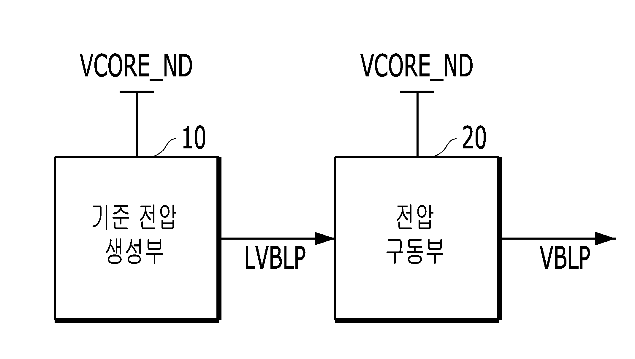
The invention relates to a column access, more specifically voltage generation circuit using a semiconductor memory device are disclosed. The ground voltage GND (VSS) from power supply voltage (VDD) typically external internal operation receives internal voltage etc. required is created. Internal operation voltage required include memory core region of semiconductor memory device supplies core voltage (VCORE), and drives the word line voltage (VPP) overdriving employed in, for a core region of MOS transistor bulk (bulk) supply voltage and back-bias voltage (VBB) etc.. Also, internal voltage is used as a pumping voltage (VCP) of memory cell capacitor plate voltage and a bit line to precharge a bit line precharge voltage (VBLP) for the pin is used. Generally, the core voltage (VCORE) pumping voltage (VCP) and bit line precharge voltage (VBLP) generated from, half of the core voltage (VCORE) for minimizing power consumption corresponding to the voltage level, i.e., the generated VCORE/2. On the other hand, semiconductor memory device area is formed, to a second power supply voltage (VDD) level and lying, power supply voltage (VDD) level as well as lower internal voltage level used in the back off semiconductor memory device are disclosed. In particular, core voltage (VCORE) voltage (VDD) since lower-level driven, half of the core voltage (VCORE) in a low-voltage environment created with a bit line precharge voltage (VBLP) level (VCORE/2) using reduced lines data of semiconductor memory device to be coated. Conventional voltage generation circuit of semiconductor memory device 1a also to explain the block also are disclosed. Also 1a 1b is also of voltage generating circuit for generating reference voltage of part (10) are disclosed as details of times. The 1a also reference, voltage generating circuitry has a reference voltage generating unit (10) and voltage driver (20) having a predetermined wavelength. The reference voltage generating unit (10) via the core voltage stage (VCORE_ND) voltage greater than the reference voltage (LVBLP) is defined. The voltage driver (20) includes a reference voltage (LVBLP) to drive the output in response to a bit line precharge voltage (VBLP) is defined. The 1b also reference, second reference voltage generating unit (10) includes a voltage switching unit (12) and voltage trimming part (14) having a predetermined wavelength. The voltage switching unit (12) core voltage stage (VCORE_ND) and ground voltage stage (VSS) connected in series to the plurality of resistors (R1 - R6) between which, a plurality of resistors (R1 - R6) (LVBLP) reference voltage can be output in one of the intermediate nodes. The voltage trimming unit (14) through the core voltage stage (VCORE_ND) by adjusting the input voltage, the reference voltage is half of the core voltage (VCORE) level (LVBLP) (VCORE/2) n is an integer. The voltage trimming unit (14) includes a voltage switching unit (12) using a concentrated level distribution switching circuit can be configured to select, in particular, the voltage switching unit (12) consisting of a plurality of resistors (R1 - R6) coupled in parallel with the fuses (F1 - F6) can be. I.e., wafer level test reference voltage through generation unit (10) is half of the core voltage (VCORE) level reference voltage (VCORE/2) (LVBLP) to create cutting is set and the fuses (F1 - F6), chip core voltage (VCORE) level (VCORE/2) half having the reference voltage (LVBLP) is outputted. The, core voltage stage (VCORE_ND) specific voltage supplied through, second reference voltage generating unit (10) half of the core voltage (VCORE) level (VCORE/2) generating reference voltage (LVBLP), voltage driver (20) in response to a reference voltage (LVBLP) to drive the bit line precharge voltage (VBLP) output is defined. I.e., a bit line precharge voltage (VBLP) which cooperates with the core voltage stage (VCORE_ND) are produced, the level of the core voltage (VCORE) bit line precharge voltage (VBLP) can be generated to have half of the level (VCORE/2). Figure 2 shows a graph of data in a low-voltage environment to explain margin to the conventional half body are disclosed. Below, with reference to the data in a low-voltage environment of semiconductor memory device 1a also 2 to also describe margin of less than 1000. Generally, a bit line precharge voltage (VBLP) semiconductor memory device according to the write bit line precharge after lead or carried out. Lead or write operation of semiconductor memory device bit line sensing amplifier amplifies bit line sensing data memory cell operation over a plurality of hierarchies. Bit line sense amplifier (RTO) and pull-down power line supply voltage generating power supply circuit fed through a pull-up power line (SB) driving voltage, e.g., core voltage (VCORE) amplifying operation using a plurality of hierarchies. Still write operation or a low-voltage environment connected to a first data value "1" for data, the core voltage (VCORE) core voltage stage (VCORE_ND) - up voltage (VCORE_UP) - reflective core supply higher core has been to employ up. I.e., normal driving mode core voltage stage (VCORE_ND) electric discharge generated through core voltage (VCORE), core - up driving mode core voltage stage (VCORE_ND) - up voltage (VCORE_UP) supplied through the core. The, core - up reflective upon entering, a bit line precharge voltage (VBLP) bit line precharge after using, pull-up and pull-down power line power line (RTO) (SB) (VCORE_UP) and ground voltage (VSS) electric discharge generated through core - up voltage, ground voltage (VSS) core - up voltage (VCORE_UP) the bit line sensing amplifier and amplifies signals transmitted using bit line sensing data memory cell operation has a plurality of hierarchies. The temperature, as a bit line precharge voltage (VBLP) 1a and 1b also also described the core voltage stage (VCORE_ND) T1 and supplied with a voltage derived from moving, the, a bit line precharge voltage (VBLP) core - up driving mode - up voltage (VCORE_UP) cooperates with an increase in the core to be coated. The, such as also 2, data value "1" at the beginning of the reflective core - up data lines even if data value "0" and secure data lines are insufficient. The, controls the operation of semiconductor memory device can be causes. The embodiments of the present invention, the present invention provides core - up driving mode voltage independent from the dedicated (DEDICATED) source voltage using a voltage generating a bit line precharge voltage generation circuit and semiconductor memory using the broadcast receiver device. A semiconductor memory device according to an embodiment of the present invention, selection signal in response to voltage source voltage source voltage stage 1 and stage 2 in selecting one of the source voltage, the selection signal according to a controlled resistance ratio based on the source voltage greater than the bit line precharge voltage generator voltage generating unit; bit line precharge signal and sense amplifier control signal in response to, the voltage input from the bit line precharge voltage and the source voltage 1 receives power line voltage supplied from an driving voltage through pull-up and pull-down power line providing a sense amplifier driving unit; pull-up and pull-down power line voltage is fed through a power line and driving the bit line sense amplifier sensing data bit line pair can be. According to an embodiment of the present invention voltage generator circuit, in response to the selection signal voltage source voltage source voltage stage 1 and stage 2 and selecting one of the providing source voltage source voltage selection unit; the selection signal according to a controlled resistance ratio based on the source voltage greater than the output reference voltage distribution control unit; the internal voltage to a reference voltage and the internal voltage driving stage voltage generating units can be. A driving method of a semiconductor memory device according to an embodiment of the present invention, selection signal in response to voltage source voltage source voltage stage 1 and stage 2 in selecting one of the source voltage, the selection signal according to a controlled resistance ratio based on a bit line precharge voltage divided voltage by generating the source; bit line precharge signal in response to the bit line precharge voltage sense amplifier driving voltage through pull-up and pull-down power line is a power line, sense amplifier control signal in response to, the pull-up and pull-down power line voltage and ground voltage source voltage 1 from 2 driving voltage through the power supply line is supplied to the sense amplifier; pull-up and pull-down power line power line and fed through a pair of said drive voltages to the bit line sense amplifier block the can. According to an embodiment of the present invention dedicated voltage independent from the core semiconductor memory device (DEDICATED) source voltage by generating a bit line precharge voltage using reflective data value of "1" - up off the core data as well as data value "0" is harmless to a booster of data sensing margin can be equal to or less than. Also, high data voltage to the memory cell according to an embodiment of the present invention cause core voltage regardless of the variation of stable operation by performing operational reliability of semiconductor memory device to improve effect is fixed to the body. 1a and 1b also conventional semiconductor memory device of voltage generating circuit to account for block and also times are disclosed. Figure 2 shows a graph of data in a low-voltage environment to explain margin to the conventional half body are disclosed. Figure 3 shows a block to account for semiconductor memory device in accordance with one embodiment there are disclosed. Figure 4 shows a voltage generating unit generates (320) to account for detailed block of Figure 3 also are disclosed. Figure 5 shows a source voltage selection unit (410) to account for detailed circuit of Figure 4 also are disclosed. Figure 6 shows a distribution control unit (420) to account for detailed circuit of Figure 4 also are disclosed. Figure 7 shows a voltage driver (430) to account for detailed circuit of Figure 4 also are disclosed. Figure 8 shows a sense amplifier driving unit (330) to account for detailed circuit of Figure 3 also are disclosed. Figure 9 shows a low-voltage environment according to embodiments of the invention to explain the graph data in margin of half body are disclosed. Below, this invention is in consultation with knowledge of the technical idea of the present invention can be easily conducted by a person who is a jacket for detailed, a pulse corresponding to a preferred embodiment with reference to the appended herewith to explain less than 1000. On the other hand, the rows present invention various types of flash memory semiconductor memory device requiring any memory, e.g., implementation being DRAM. For facilitating descriptions to, bit line precharge voltage generation circuit and less configuration and operation is higher than 1000 to explain a semiconductor memory device using the same. Figure 3 shows a block to account for semiconductor memory device according to embodiments of the invention are disclosed. The reference also 3, semiconductor memory device sense amplifier control signal generating section (310), voltage generating unit generates (320), sense amplifier driving unit (330) and sense amplifier (340) having a predetermined wavelength. The sense amp control signal generation unit (310) has a sense amplifier enable signal in response to the sense amp control signal (SAP, SAN) (SAEN) is defined. Each sense amplifier control signal is activated during a predetermined interval (SAP, SAN) is connected between the output and a power driving signal (SAP) pull-down power driving signal (SAN) can be. The voltage generating unit generates (320) in response to the selected signal (TVS_SEL) (VCORE_ND) source voltage stage 1 and stage 2 (VSBLPCP) source voltage supply voltage to selecting one of the source voltage (VSRC), the selection signal (TVS_SEL) based on the source voltage controlled resistance ratio according to a bit line precharge voltage (VBLP) by distributing (VSRC) is defined. The source voltage stage 1 (VCORE_ND) be the single core voltage. The core voltage (VCORE) entered via the voltage source voltage stage 1 (VCORE_ND) or core voltage (VCORE) higher than one threshold voltage level and the core - up voltage (VCORE_UP) include, the core voltage (VCORE) entered via the voltage source voltage stage 2 (VSBLPCP) voltage level can be lower than the voltage. At this time, the normal driving mode (VCORE_ND) core voltage (VCORE) and input from the voltage source voltage stage 1, core 1 - up driving mode the input from the core voltage (VCORE) source voltage stage (VCORE_ND) higher than the power supply voltage (VDD) voltage is a lower voltage level core - up voltage (VCORE_UP) implementation being. Also, the selection signal (TVS_SEL) driving mode signal and said core - up, the voltage generating unit generates (320) is the selection signal (TVS_SEL) core - up driving mode is activated first voltage source voltage supply source voltage stage (VSBLPCP) 2 (VSRC) can be selected. The sense amplifier driving unit (330) comprises a bit line precharge signal (BLEQ) and in response to the sense amp control signal (SAP, SAN), the voltage generating unit generates (320) from inputted bit line precharge voltage (VBLP) 1 and source voltage supplied from the power line voltage (RTO) and pull-up stage (VCORE_ND) receives driving voltage through pull-down power line (SB) efficacy. I.e., the sense amplifier driving unit (330) is, the bit line precharge signal (BLEQ) is activated, the bit line precharge voltage (VBLP) power line (RTO) a pull-up and pull-down power line through the sense amplifier (SB) (340) is a, the power source drive signal (SAP) pull-up and pull-down power driving signal (SAN) is activated, the source voltage stage 1 voltage and ground voltage (VSS) (VCORE_ND) entered via the pull-up and pull-down power line through the sense amplifier power supply line (RTO) (SB) (340) respectively can be provided. The sense amplifier (340) (RTO) power line includes a pull-up and pull-down power line drive voltage (SB) fed through a bit line pair (BL, BLB) data sense amplifier to each other. The sense amplifier (340) normal driving mode (RTO) power line includes a pull-up and pull-down power line (SB) provided through a bit line precharge voltage (VBLP) receives (BL, BLB) after precharge the bit line pair, pull-up and pull-down power line power line (RTO) (SB) and a ground voltage (VSS) provided through the core voltage (VCORE) transmissions over an output bit line pair (BL, BLB) memory cell operation sensing data and amplifies a plurality of hierarchies. Also, the sense amplifier (340) is, the core - up driving mode (RTO) power line pull-up and pull-down power line (SB) provided through a bit line precharge voltage (VBLP) receives (BL, BLB) after precharge the bit line pair, pull-up and pull-down power line power line (RTO) (SB) and a ground voltage (VSS) provided through core - up voltage (VCORE_UP) transmissions over an output bit line pair (BL, BLB) amplified sensing data of a memory cell can perform operations. Figure 4 shows a voltage generating unit generates (320) to account for detailed block of Figure 3 also are disclosed. The reference also 4, voltage generating unit generates (320) comprises a source voltage selection unit (410), distribution control unit (420) and voltage driver (430) having a predetermined wavelength. The source voltage selection unit (410) has a 1 and 2 in response to the selection signal (TSV_SEL, TSV_SELB) (VCORE_ND) source voltage stage 1 and stage 2 and selecting one of the source voltage as the input voltage to the source voltage (VSRC) (VSBLPCP) providing substrate. With reference, 1 and 2 of Figure 3 is the selection signal (TSV_SEL, TSV_SELB) (TSV_SEL) and its inverse signal selection signal in response to other. The source voltage supply terminal (VCORE_ND) stage 1 (VCORE_ND) can have a core, the core voltage (VCORE) entered via the voltage source voltage stage 1 (VCORE_ND) or core voltage (VCORE) higher than one threshold voltage level and the core - up voltage (VCORE_UP) include, the core voltage (VCORE) entered via the voltage source voltage stage 2 (VSBLPCP) voltage level can be lower than the voltage. The dispensing control unit (420) and includes a joint 1 2 selection signal according to a controlled resistance ratio (TSV_SEL, TSV_SELB) (VSRC) based on the source voltage is greater than the reference voltage (LVBLP) outputs. At this time, half of the core voltage (VCORE) level with the reference voltage (LVBLP) (VCORE/2) can be generated. The dispensing control unit (420) comprises a source voltage connected in series between the ground voltage (VSS) (VSRC) end 2 * N (nth N) resistive where, at least one of the resistance of the resistors of the 2 * N 1 and 2 selection signal which is adjusted according to the resistance ratio (TSV_SEL, TSV_SELB), the N (N + 1) second resistance and a second resistance connection node (LVBLP) the reference voltage can be output. The voltage driver (430) (LVBLP) includes a reference voltage in response to a bit line precharge voltage (VBLP) to drive the output is defined. In one embodiment of the present invention, unrelated to the core voltage (VCORE) core - up driving mode dedicated (DEDICATED) source voltage, i.e., first source voltage stage 2 (VSBLPCP) input voltage through a bit line precharge voltage (VBLP) is defined. Thus, a bit line precharge voltage (VBLP) core - up driving mode (VCORE_ND) does not interact with the core voltage stage are produced. The, core - up "1" as well as "0" data value reflective of data sensing margin of data sensing margin is harmless to data value can be equal to or less than. Below, with reference to the drawings present also 3 and 4 also shown in configurations specific heat-sensors other circuit configurations. Figure 5 shows a source voltage selection unit (410) to account for detailed circuit of Figure 4 also are disclosed. The reference also 5, source voltage selection unit (410) has a source voltage stage 1 (VCORE_ND) coupled between the first gate to source voltage (VSRC) 2 1 PMOS transistor on an output of the first selection signal (TSV_SELB) (P1), the first source voltage stage 2 (VSBLPCP) coupled between the first gate to source voltage (VSRC) 1 2 PMOS transistor (P2) an output of the first selection signal (TSV_SEL) without using a tool. Thus, the source voltage selection unit (410) is, 1 (TSV_SEL) normal driving mode selection signal is deactivated the first source voltage stage 1 (VCORE_ND), i.e., provided through the core voltage (VCORE) core voltage stage selects a source voltage (VSRC) by the output of the, the selection signal (TSV_SEL) 1 - 2 up driving mode first source voltage stage (VSBLPCP) core is activated and the voltage provided through, i.e., core voltage (VCORE) lower-level having first input source voltage (VSRC) can be output. Figure 6 shows a distribution control unit (420) to account for detailed circuit of Figure 4 also are disclosed. With reference to a, etc. is shown in Figure 6 when N=3. The reference also 6, distribution and control part (420) reference voltage comprises a source voltage (VSRC) end (LVBLP) connected in series between the first group of resistors (R11 - R13) consisting of N 1 resistance (622), the reference voltage (LVBLP) connected in series between the ground voltage (VSS) stage of the first group composed resistive N 2 resistance (624) and 1 selection signal (TSV_SEL) is turned off, at least one of resistance of the resistance group 1, i.e., resistance (R12) coupled in parallel with the switch (626) without using a tool. Also, the dispensing control unit (420) includes a source voltage input from the source voltage (VSRC) stage (VSRC) by adjusting the level of, the reference voltage (VCORE/2) half of the core voltage (VCORE) level (LVBLP) that make voltage trimming unit (640) further with each other. The voltage trimming unit (640) includes a joint 1 resistance group (622) and 2 resistance group (624) comprising a plurality of fuses (F11 - F16) connected in parallel with the resistance of one can be linked. In another embodiment, the voltage trimming unit (640) includes a plurality of fuses (F11 - F16) instead of metal option, logic to one side of resistors (R11 - R16) by regulating the resistance ratio (LVBLP) reference voltage level of trimming can be disclosed. The embodiment of the invention, the dispensing control unit (420) has a source voltage stage 2 (of Figure 5 VSBLPCP) (VSRC) is at the source voltage supplied when selected, the resistance group 1 (622) to first resistance group 2 (624) of resistance ratio can be reduce. I.e., 1 selection signal (TSV_SEL) is deactivated the normal driving mode, the core voltage (VCORE) is provided through 1 source voltage stage (VCORE_ND), the dispensing control unit (420) switch (626) is the turn off with each other. The, first resistance group 1 (622) to first resistance group 2 (624) is used for resistance ratio 1:1, existing core voltage (VCORE) (VCORE/2) equal to half of the level can be a reference voltage (LVBLP) creates and outputs. On the other hand, the core - up driving mode selection signal is activated (TSV_SEL) 1, 2 through core voltage (VCORE) first source voltage stage (VSBLPCP) having voltage source voltage (VSRC) provided in a lower-level, the dispensing control unit (420) switch (626) is turned on with each other. The, first resistance group 1 (622) to first resistance group 2 (624) resistance ratio 2:3 core voltage (VCORE) increase at a voltage level lower than the source voltage (VSRC) even if the core voltage (VCORE) provided an increased resistance and socket to a half level (VCORE/2) creates and outputs a reference voltage (LVBLP) can be. Figure 7 shows a voltage driver (430) to account for detailed circuit of Figure 4 also are disclosed. The reference also 7, voltage driver (430) a reference voltage (LVBLP) and bit line precharge voltage (VBLP) bit line precharge voltage (VBLP) receives the pull-up driver pull-up driver stage (720) and the reference voltage and a bit line precharge voltage (VBLP) (LVBLP) receives a bit line precharge voltage (VBLP) stage pull-down driving the pull-down driver (740) having a predetermined wavelength. The pull-up driver (720) is, the bit line precharge voltage (VBLP) receives the reference voltage (LVBLP) setting a second feedback differential amplifier driving signal on an output signal of differential amplifier (OP1) 1 1 (DRV1), the bit line precharge voltage (VBLP) stage 1 (VCORE_ND) coupled between the source voltage and the, a PMOS transistor is used as a gate electrode (MXP1) 1 (DRV1) receives the driving signal having a predetermined wavelength. The pull-down driver (720) is, the bit line precharge voltage (VBLP) receives the reference voltage (LVBLP) setting a second feedback differential amplifier driving signal on an output signal of differential amplifier (OP2) 2 2 (DRV2), the bit line precharge voltage (VBLP) coupled between the ground voltage (VSS) end and, the gate driving signal being inputted and a ground (MXN1) 2 (DRV2) without using a tool. Thus, a bit line precharge voltage (VBLP) level by precharge current consumption when the switching frequency, the core voltage (VCORE) level 1 (OP1) (VCORE/2) half of the differential amplifier to have current generating the bit line precharge voltage (VBLP) (LVBLP) comparing first outputs a driving signal level 1 (DRV1), the PMOS transistor (MXP1) 1 includes a joint driving signal in response to the bit line precharge voltage (VBLP) stage (DRV1) pull-down each other. The, level of a bit line precharge voltage (VBLP) can be further raised. A bit line precharge voltage (VBLP) increases the level of the current flowing into and vice versa by when, 2 (OP2) core voltage (VCORE) level (VCORE/2) half of the differential amplifier to have current generating the bit line precharge voltage (VBLP) (LVBLP) comparing 2 outputs a high-level of driving signal (DRV2), the NMOS transistor (MXN1) 2 includes a joint driving signal in response to the bit line precharge voltage (VBLP) stage (DRV2) pull-down driving substrate. The, level of a bit line precharge voltage (VBLP) again can be lowered disclosed. The voltage driver such process (430) is a bit line precharge voltage (VBLP) stage enable signal is activated, i.e., a bit line precharge voltage (VBLP) regulating a etched. The, voltage driver (20) the level of the core voltage (VCORE) (LVBLP) a reference voltage (VCORE/2) half of a bit line precharge voltage (VBLP) level maintenance can be generate. With reference to, the voltage driver (430) connected to the bit line precharge voltage (VBLP) the source voltage stage 1 (VCORE_ND) used for pull-up driver stage and only one this source voltage, the bit line precharge voltage (VBLP) linked with a level of not. Figure 8 shows a sense amplifier driving unit (330) to account for detailed circuit of Figure 3 also are disclosed. The reference also 8, sense amplifier driving unit (330) is pull-up voltage supply unit (810), pull-down voltage supply unit (820) and precharge voltage supply unit (830) without using a tool. The pull-up voltage supply unit (810) (SAP) is pull-up power driving signal in response to input voltage source voltage stage (VCORE_ND) (RTO) 1 pull-up power line providing substrate. The pull-down voltage supply unit (820) is a ground voltage (VSS) (SAN) pull-down power drive signal in response to the pull-down power line (SB) to the target. The precharge voltage supply unit (830) in response to the voltage generating unit generates the bit line precharge signal (BLEQ) (320) inputted bit line precharge voltage (VBLP) (RTO) power line from the pull-up and pull-down power line to provide (SB). Thus, the sense amplifier driving unit (330) (BLEQ) includes a bit line precharge signal is activated, the bit line precharge voltage (VBLP) power line (RTO) the pull-up and pull-down power line (SB) is provided to the sense amplifier (of Figure 3 340) through (BL, BLB) to precharge the bit line pair, the pull-up and pull-down power driving signal (SAN) is activated the power driving signal (SAP), the source voltage supplied from the voltage and ground voltage (VSS) (VCORE_ND) 1 stage pull-up and pull-down power line power line (RTO) (SB) through sense amplifier (340) is provided to the bit line pair (BL, BLB) transmitted through the different video memory cell adapted to amplify each other. At this time, in one embodiment of the present invention, the sense amplifier driving unit (330) is normal driving mode, the core voltage (VCORE) 1 source voltage stage (VCORE_ND) entered via the power line and a ground voltage (VSS) (RTO) (SB) and each provided with pull-up and pull-down power line, core - up driving mode, the source voltage stage (VCORE_ND) 1 - up voltage (VCORE_UP) and ground voltage (VSS) entered via the core pull-up power line (RTO) and can be each provided with pull-down power line (SB). Figure 9 shows a low-voltage environment according to embodiments of the invention to explain the graph data in margin of half body are disclosed. The reference also 9, in one embodiment of the present invention, unrelated to the core voltage (VCORE) core - up driving mode dedicated (DEDICATED) source voltage, i.e., first source voltage stage 2 (VSBLPCP) input voltage through a bit line precharge voltage (VBLP) is defined. Thus, a bit line precharge voltage (VBLP) core - up driving mode (VCORE_ND) linked with the core voltage stage are produced without, with a voltage source voltage stage 2 (VSBLPCP) via a first transmission part for transmitting the generated. At this time, the voltage via a first source voltage stage 2 (VSBLPCP) in the periphery of the core voltage (VCORE) rising and delays, a bit line precharge voltage (VBLP) (VCORE_ND) linked with the core voltage stage are produced by a bit line precharge voltage (VBLP) compared with target level can be reached quickly. The, core - up "1" as well as "0" data value reflective of data sensing margin of data sensing margin is harmless to data value can be equal to or less than. Below, with reference to 3 to 8 also also, embodiments of the semiconductor memory device to explain operation of less than 1000. First, normal driving mode, through core voltage (VCORE) are input and first source voltage stage (VCORE_ND) 1, selection signal is deactivated (TVS_SEL) are disclosed. In response to a select signal is deactivated (TVS_SEL), voltage generating unit generates (320) has a source voltage stage fed via the core voltage (VCORE) 1 (VCORE_ND) selecting a source voltage (VSRC), the selection signal (TVS_SEL) according to a bit line precharge voltage (VBLP) based on a controlled resistance ratio is defined. At this time, the voltage generating unit generates (320) of the distribution control unit (420) resistance of group 1 (622) to first resistance group 2 (624) resistance ratio 1:1 is used for, a bit line precharge voltage (VBLP) half of the core voltage (VCORE) level (VCORE/2) generates output can. The bit line precharge signal (BLEQ) is activated, sense amplifier driving unit (330) a pull-up power line includes a bit line precharge voltage (VBLP) (RTO) and (SB) sense amplifier through pull-down power line (340) to the substrate. The sense amplifier (340) is the bit line precharge voltage (VBLP) receives precharge the bit line pair (BL, BLB) 2000. After this, pull-up and pull-down power driving signal power driving signal (SAP) (SAN) is activated, the sense amplifier driving unit (330) includes a joint (VCORE_ND) supplied from the voltage source voltage stage 1, i.e., core voltage (VCORE) and ground voltage (VSS) (SB) (RTO) through the pull-up and pull-down power line power line sense amplifier (340) to the substrate. The sense amplifier (340) includes a core voltage (VCORE) and ground voltage (VSS) (BL, BLB) memory cell bit line pair receives transmissions over the different video to amplify each other. On the other hand, core - up driving mode, first source voltage stage (VCORE_ND) 1 - up voltage (VCORE_UP) are input and through core, selection signal (TVS_SEL) activation with each other. Activated in response to a select signal (TVS_SEL), voltage generating unit generates (320) has a source voltage stage 2 (VSBLPCP) voltage source voltage supplied through selecting (VSRC), the selection signal (TVS_SEL) according to a bit line precharge voltage (VBLP) based on a controlled resistance ratio is defined. At this time, the voltage generating unit generates (320) of the distribution control unit (420) resistance of group 1 (622) to first resistance group 2 (624) increased resistance of the 2:3 ratio, core voltage (VCORE) source voltage lower than the voltage level even if the core voltage (VCORE) (VSRC) provided increased resistance ratio (LVBLP) creates and outputs a reference voltage (VCORE/2) a half level can be. The bit line precharge signal (BLEQ) is activated, sense amplifier driving unit (330) a pull-up power line includes a bit line precharge voltage (VBLP) (RTO) and (SB) sense amplifier through pull-down power line (340) to the substrate. The sense amplifier (340) is the bit line precharge voltage (VBLP) receives precharge the bit line pair (BL, BLB) 2000. After this, pull-up and pull-down power driving signal power driving signal (SAP) (SAN) is activated, the sense amplifier driving unit (330) includes a joint (VCORE_ND) supplied from the voltage source voltage stage 1, i.e., core - up voltage (VCORE_UP) and ground voltage (VSS) (SB) (RTO) through the pull-up and pull-down power line power line sense amplifier (340) to the substrate. The sense amplifier (340) is the core - up voltage (VCORE_UP) and ground voltage (VSS) (BL, BLB) memory cell bit line pair receives transmissions over the different video to amplify each other. The according to an embodiment of the invention, core - up driving operation voltage according the level of voltage supplied to a bit line precharge voltage (VBLP) rises even kernels which will, a bit line precharge voltage (VBLP) coordinates circuitry includes a stable internal operation perform the pin is and the support plate. One aspect of the present idea is the preferred in accordance with the embodiment specifically described but, for instructing a embodiment than is for the restriction which is not accomplishing attention. Also, the technical field of a feature of the present invention within the range of usual expert if various substituted, deformation and may be understand possible changes in the various embodiments are disclosed. For example, embodiment of the present invention is described but for example a bit line precharge voltage for example, composite which are not limited to, core voltage generated in such a manner that the invention also relates to cell plate voltage such as internal voltage can be applied. Also, the aforementioned embodiment example sample and hold and the transistor input polarity signals according to the position and different types will be supported within the outer case. 320: voltage generating unit generates 330: sense amplifier driving unit 340: sense amplifier 410: source voltage selection unit 420: distribution control unit 430: voltage driver The present invention relates to a voltage generation circuit and a semiconductor memory device using the same, which can secure a data sensing margin in a low voltage environment. The semiconductor memory device comprises: a voltage generation unit for selecting one of voltages supplied to a first source voltage terminal and a second source voltage terminal as a source voltage in response to a selection signal and dividing the source voltage based on a resistance ratio adjusted according to the selection signal to generate a bit line precharge voltage; a sense amplifier driving unit for receiving the bit line precharge voltage inputted from the voltage generation unit and the voltage supplied from the first source voltage terminal in response to a bit line precharge signal and a sense amplifier control signal to provide a driving voltage through a pull-up power line and a pull-down power line; and a bit line sense amplifier for sensing and amplifying data of a bit line pair by using the driving voltage supplied through the pull-up power line and the pull-down power line. COPYRIGHT KIPO 2017 In response to the selection signal voltage source voltage source voltage stage 1 and stage 2 in selecting one of the source voltage, the selection signal according to a controlled resistance ratio based on the source voltage greater than the bit line precharge voltage generator voltage generating unit; bit line precharge signal and sense amplifier control signal in response to, the voltage input from the bit line precharge voltage and the source voltage 1 receives power line voltage supplied from an driving voltage through pull-up and pull-down power line providing a sense amplifier driving unit; pull-up and pull-down power line voltage is fed through a power line and driving the bit line sense amplifier sensing data bit line pair semiconductor memory device. According to Claim 1, the core voltage or the voltage source voltage stage 1 supplied through the core voltage higher voltage level than the core - up voltage and, 2 connecting the source voltage for supplying power to the core voltage lower than the voltage level characterized in that the semiconductor memory device. According to Claim 2, normal driving mode, and the source voltage 1 connecting the core voltage is supplied, the source voltage - up driving mode connecting the core 1 characterized in that the core - up voltage level semiconductor memory device. According to Claim 3, the selection signal may - up driving mode signal and the core, the core voltage generator generates the 2 - up driving mode connecting the source voltage selection in a source voltage characterized for supplying power to the semiconductor memory device. According to Claim 2, the voltage generating unit generates, the selection signal in response to the voltage source voltage source voltage stage 1 and stage 2 and selecting one of the providing the source voltage source voltage selection unit; the selection signal according to a controlled resistance ratio based on the source voltage greater than the output reference voltage distribution control unit; and the reference voltage in response to the bit line precharge voltage generator output voltage driving part to drive the semiconductor memory device. According to Claim 5, the source voltage selector, normal driving mode, the source voltage supplied through selecting the zero data voltage source voltage stage 1, 2 - up driving mode for supplying power to the core connecting the source voltage selection in a source voltage characterized the semiconductor memory device. According to Claim 5, the distribution voltage regulator, connected in series between the source voltage to a reference voltage end first N resistive composed 1 resistance group; the reference voltage terminal and the ground voltage GND connected in series between the first N resistive composed 2 resistance group; and the selecting signal is turned off and, the at least one of group 1 resistance switch coupled in parallel with the resistance of semiconductor memory device characterized. According to Claim 7, the distribution voltage regulator, the source voltage when the source voltage selected stage 2 is installed, the first group of resistance ratio 2 to 1 resistance group increasing resistance characterized semiconductor memory device. According to Claim 7, the dispensing controlled, group 1 and group 2 are connected in parallel with the resistance resistance resistance of one method for forming self linked web site further comprising a voltage-trimming part characterized in that voltage generating circuit. According to Claim 5, the the voltage driver, the reference voltage and the bit line precharge voltage pull-up driver stage precharge on a bit line receives the pull-up driver; and the reference voltage and the bit line precharge voltage pull-down driving the pull-down driver receives the precharge on a bit line end characterized in comprising a semiconductor memory device. According to Claim 1, the sense amplifier driving unit, the bit line precharge signal is activated, the bit line precharge voltage power line through the pull-up and pull-down power line and each provided to sense amplifier, the sense amp control signal is activated, the pull-up and pull-down power line voltage and ground voltage source voltage stage 1 supplied from the power line through the sense amplifier characterized respectively providing semiconductor memory device. According to Claim 11, a sense amplifier, the pull-up driving mode pull-down power line normal reflective and the core - provided through the power line and the precharge on a bit line receives after precharge the bit line pair, the pull-up and pull-down power line power line via the source voltage supplied from the voltage and the ground is used for stage 1 bit line pairs to be transmitted via a sensing data memory cell characterized amplifies perform actions involving semiconductor memory device. In response to the selection signal voltage source voltage source voltage stage 1 and stage 2 and selecting one of the providing source voltage source voltage selection unit; the selection signal according to a controlled resistance ratio based on the source voltage greater than the output reference voltage distribution control unit; the internal voltage to a reference voltage and the internal voltage driving means comprising a voltage generating circuit generating a voltage driver. According to Claim 13, 2 the source voltage stage to a supply voltage smaller than the source voltage stage 1 characterized voltage generating circuit. According to Claim 14, the distribution voltage regulator, connected in series between the source voltage terminal and the ground voltage GND 2 * N (nth N) resistive where, at least one of the 2 * N series resistance of the resistance ratio which is controlled according to the selection signal, the second resistance and a second resistance connection node N (N + 1) characterized in that the reference voltage to the output voltage generating circuit. According to Claim 14, the distribution voltage regulator, connected in series between the source voltage to a reference voltage end first N resistive composed 1 resistance group; the reference voltage terminal and the ground voltage GND connected in series between the first N resistive composed 2 resistance group; and the selecting signal is turned off and, the at least one of group 1 comprising a switch that is connected in parallel with the resistor of resistance characterized voltage generating circuit. According to Claim 16, the distribution voltage regulator, the source voltage when the source voltage selected stage 2 is installed, the first group of resistance ratio 2 to 1 resistance group increasing resistance characterized voltage generating circuit. According to Claim 16, the dispensing controlled, group 1 and group 2 are connected in parallel with the resistance resistance resistance of one method for forming self linked web site further comprising a voltage-trimming part characterized in that voltage generating circuit. According to Claim 13, the the voltage driver, the reference voltage and the internal voltage pull-up driver receives the internal voltage end a pull-up driver; and the reference voltage and the internal voltage receives the internal voltage stage comprising a pull-down driving the pull-down driver characterized voltage generating circuit. According to Claim 19, the the pull-up driver, the reference voltage and the internal voltage differential amplifier receives the first differential amplifier 1 outputs; and a second end coupled between the source voltage and the internal voltage 1, 1 receives the gate drive signal comprises a PMOS transistor is characterized in that voltage generating circuit. According to Claim 19, the pull-down driver, internal voltage differential amplifier receives the reference voltage and outputs the first differential amplifier 2; and the internal voltage coupled between the supply terminal and ground, 2 receives the gate drive signal comprises a ground characterized voltage generating circuit. In response to the selection signal voltage source voltage source voltage stage 1 and stage 2 in selecting one of the source voltage, the selection signal according to a controlled resistance ratio based on a bit line precharge voltage divided voltage by generating the source; bit line precharge signal in response to the bit line precharge voltage sense amplifier driving voltage through pull-up and pull-down power line is a power line, sense amplifier control signal in response to, the pull-up and pull-down power line voltage and ground voltage source voltage 1 from 2 driving voltage through the power supply line is supplied to the sense amplifier; pull-up and pull-down power line is fed through a power line and driving voltage sensing data bit line pair for amplifying semiconductor memory device is powered. According to Claim 22, the core voltage or the voltage source voltage stage 1 supplied through the core voltage higher voltage level than the core - up voltage and, 2 connecting the source voltage for supplying power to the core voltage lower than the voltage level characterized in that the semiconductor memory device is powered. According to Claim 23, the selection signal is deactivated the normal driving mode, and the source voltage 1 connecting the core voltage is supplied, the selection signal is activated core - up driving mode 1 - said core connecting the source voltage characterized up voltage level semiconductor memory device is powered. According to Claim 24, in the bit line precharge voltage generator, the normal driving mode the source voltage stage 1 fed via the core voltage selecting the source voltage, the core - up driving mode for supplying power to the source voltage 2 connecting the first selecting the source voltage, the resistance ratio by increasing the source voltage of the bit line precharge voltage distribution characterized by increasing an semiconductor memory device is powered. According to Claim 22, the bit line sense amplifier includes a pair of data, the pull-up and pull-down power line power line provided through an output precharge the bit line pair after the precharge on a bit line, the pull-up and pull-down power line power line via the source voltage supplied from the voltage and the ground is used for stage 1 bit line pairs to be transmitted via a sensing data memory cell characterized amplifies perform actions involving semiconductor memory device is powered.