METHOD FOR MANUFACTURING SEMICONDUCTOR PACKAGE
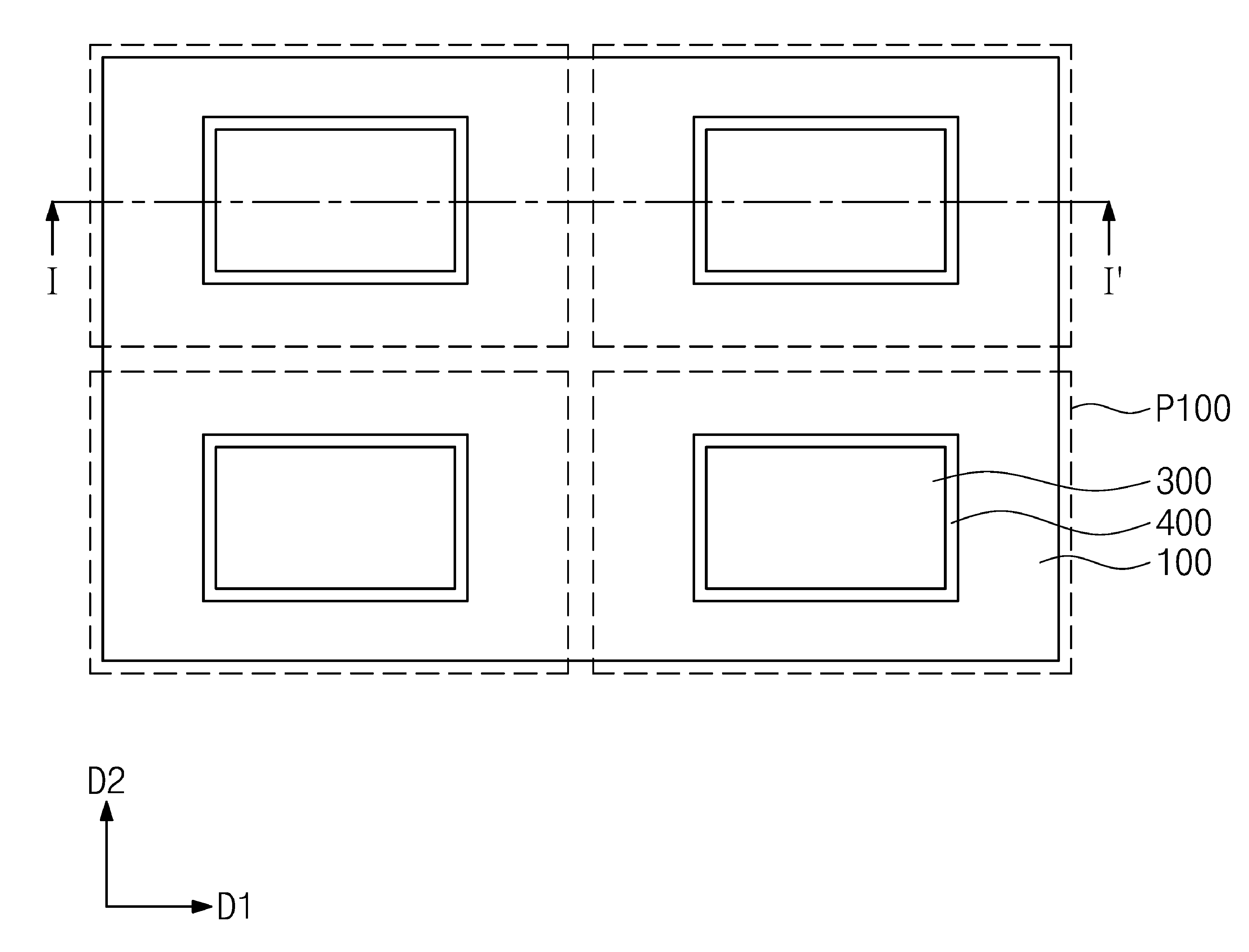
The present invention refers to semiconductor package and number bath method relates to, a substrate including semiconductor package and number is provided to a bath method are disclosed. Semiconductor package includes an integrated circuit chip embodied in the form suitable for use in electronic number article are disclosed. Recently by the electronics industry's development, a small-sized semiconductor package, weight, number of obtaining various directions to the question and tms320c6701. [...] economize in the component. The size of the semiconductor chip by the reduction etc. highly integrated semiconductor chip. However semiconductor chip by an small, plastic prepared in a desired solder ball, solder ball also difficult handling and test vehicle from the outside. In accordance with the size of the semiconductor chip mounting board with multi-door number actually measured disclosed. In order to solve number is same fanout panel level package (Fan a-out panel level package) was not. By semiconductor package is miniaturized, bending of the semiconductor package (warpage) this door number is coming in now. The present invention is a process for preparing and number if the number is formed between the second plate carrier can be generated between a number of semiconductor package [...] bath method number 30 to 60 seconds. The present invention is the number to one or more pipeline and number and number if not, another and number are not mentioned below may be clearly understand one skilled from the substrate are disclosed. According to the above-mentioned number of semiconductor package of the present invention in the embodiment for solving technological and number bath method is joined in a hole passing through its internal substrate formed, forming a connecting substrate below said carrier substrate number 1, number [...] said hole during manufacture of a semiconductor chip, said semiconductor chip and said printed layer pattern formed thereon by applying a molding member on molding, molding said adhesion layer on number 2 fitted on the carrier substrate, the carrier substrate surface and said lower surface of said stand-alone said number 1 number of semiconductor chip to expose the connecting substrate, a substrate formed below said semiconductor chip and said printed-circuit cards, said number 2 separating the carrier substrate from said adhesive layer, said adhesive layer and a number can be a stand-alone. According to the above-mentioned number of semiconductor package of the present invention in the embodiment for solving technological and number are fixed semiconductor chips on a substrate film a number [...] molding tank connection method, a flat surface formed on said carrier substrate molding, said printed-circuit and said semiconductor chips formed on a substrate, said projection protruding into said adhesive layer to form a adhesive layer on the upper side, said carrier substrate separate from said adhesive layer, said adhesive layer and a number can be a stand-alone. According to the method of the present invention in the embodiment of semiconductor package are tank number, number 2 from carrier substrate using a second adhesive layer formed over front side adhesive layer can be separated and, thereby externally applied physical adhesion adhesive layer number 1308. without wetting ability. The, number 1 and number 2 separated from the molding layer to carrier substrate for hereinafter, number 2 (warpage) bending of semiconductor package carrier substrate filtering process during thereof can will not occur. In addition, since the number 2 without disabling the carrier substrate, the carrier substrate number 2 can be recycled. In the embodiment shown in plane view according to number of semiconductor package are also 1a is bath process are disclosed. In the embodiment shown is also 1b are plane view according to number 1 package are disclosed. In the embodiment according to the number of semiconductor package are also 2j 2a to also to explain the cross-sectional drawing bath process are disclosed. 3A to 3c is also 2g A region of drawing for the enlargement also are disclosed. Hereinafter, with reference to the method of the present invention general outline according to number of semiconductor package are drawing bath are described substrate. In the embodiment shown in plane view according to number of semiconductor package are also 1a is bath process are disclosed. In the embodiment shown is also 1b are plane view according to number 1 package are disclosed. In the embodiment according to the number of semiconductor package are also 2j 2a to also to explain the cross-sectional drawing bath process are disclosed. Also 2a to 2i is also 1a I a-I also of 'along a line corresponding to the sections and 16, II a-II also is also 2j 1b of' cross section along line corresponding with each other. The reference also 1a and 2a also, printed-circuit (100) is 1308. ball number. Printed-circuit (100) includes a base layers (110) and base layers (110) in conductive portion (120) can be a. In one example, printed circuit board (PCB) substrate connected (100) can be used. Conductive portion (120) at the bottom pads (121), wiring pattern (122), vias (123) and an upper pads (124) can be comprising. Lower pads (121) comprises a connecting substrate (100) surface of (100b) can be disposed on. Vias (123) base layers (110) through at least one can be. Wiring pattern (122) base layers (110) interposed between, vias (123) can be connected. Upper pads (124) comprises a connecting substrate (100) upper surface of (100a) on ball number is, vias (123) can be connected to at least one of. Upper pads (124) a wiring pattern (122) and vias (123) downward through pads (121) can be electrically connected. Upper pads (124) the lower pads (121) and number 3 (D3) are not aligned with the direction along be. Here, number 3 direction (D3) is joined in a substrate (100) surface of (100b) in a direction perpendicular, number 1 direction (D1) and (D2) number 2 direction connection substrate (100) surface of (100b) direction parallel can be defined. (D1) (D2) can be the direction intersecting the direction number 1 number 2. The reference also 1a and also 2b, printed-circuit (100) a hole in (101) can be formed. Hole (101) comprises a connecting substrate (100) direction through a number 3 (D3) and, printed-circuit (100) can be formed by a partial section of a stand-alone number. For example, hole (101) is a step for forming a drilling (drilling) process, such as laser ablation (laser ablation) process or laser cutting (laser cutting) can be accomplished through the etching process. Said number to a connector substrate wetting ability (100) which carry number 1 in a partial area of the semiconductor chip (300, also 2d reference) the number can be co space. Hole (101) comprises a connecting substrate (100) surface of (100b) and a rear end (100a) connecting the open hole (open hole) form may have. The reference also 1a and 2c also, printed-circuit (100) is number 1 carrier substrate (200) on ball number can be disclosed. Printed-circuit (100) is number 1 carrier substrate (200) can be attached. For example, number 1 carrier substrate (200) can be an adhesive tape. Or, unlike shown, carrier substrate number 1 (200) connected to the substrate (100) is further number (not shown) between the ball member can also be disclosed. The reference also 1a and also 2d, number 1 semiconductor chip (300) is number 1 carrier substrate (200) on ball number can be disclosed. Number 1 semiconductor chip (300) includes a connection substrate (100) of holes (101) in 1308. ball number. The, number 1 semiconductor chip (300) is number 1 carrier substrate (200) can be attached. Number 1 semiconductor chip (300) is arranged in a lower section of a chip number 1 (310) may have a. A chip number 1 (310) is number 1 carrier substrate (200) can be toward. Number 1 semiconductor chip (300) comprising silicon (Si) can be. According to of the present invention in the embodiment, 2d also number 1 of semiconductor chip (300) also 2c the placement of printed-circuit (100) performed prior to placement of disapproval. In this case, number 1 semiconductor chip (300) is number 1 carrier substrate (200) is arranged on, hole (101) is number 1 semiconductor chip (300) for alignment with a, printed-circuit (100) is number 1 carrier substrate (200) can be disposed on. The reference also 1a and also 2e, number 1 molding layer (400) is number 1 carrier substrate (200) can be formed on. Specifically, printed-circuit (100) and number 1 semiconductor chip (300) molding member on a stage (not shown), said curing molding member (not shown) number 1 molding layer (400) can be formed. Number 1 molding layer (400) includes a connection substrate (100) upper surface of (100a) and number 1 semiconductor chip (300) the upper surface of (300a) covering disclosed. The, connection substrate molding member (100) and number 1 semiconductor chip (300) to be drawn between, number 1 molding layer (400) includes a connection substrate (100) and number 1 semiconductor chip (300) can be between fill. A molding member (not shown) is ABF (Ajinomoto Build provided up Film) can be. Or, (not shown) is a molding member for insulating polymer or thermosetting resin such as epoxy polymer (epoxy polymer) such as (thermosetting resin) at a disapproval. The reference also 1a and also 2f, number 1 molding layer (400) number 2 on carrier substrate (510) is 1308. ball number. Specifically, carrier substrate number 2 (510) adhesion (520) using number 1 molding layer (400) can be attached. Adhesive layer (520) comprising expandable adhesive number (foamable adhesive) can be. For example, ultraviolet (UV) or by heat expandable foam can be a number (blowing agent). Carrier substrate number 2 (510) can be the substrate of the rigid material. For example, carrier substrate number 2 (510) can be transparent substrate such as a glass substrate. Or, adhesive layer (520) including a foam when heat number, carrier substrate number 2 (510) solid polymer of the substrate may be filled. Carrier substrate number 2 (510) which carry connecting substrate in the (100) surface of (100b) and number 1 semiconductor chip (300) surface of (300b) number 1 on substrate (600) during the formation, printed-circuit (100) and number 1 semiconductor chip (300) for supporting, printed-circuit (100) can be prevent bending of occurrence (warpage). Then, as shown in dashed lines also 2f, carrier substrate number 1 (200) to the number of special paper, semiconductor chip number 1 (300) surface of (300b) and printed-circuit (100) surface of (100b) can be exposed. Number 1 carrier substrate (200) (not shown) bonded onto member if there is, in addition number 1 (not shown) adhesive member carrier substrate (200) with special number can be disclosed. The reference also 1a and also 2g, number 1 semiconductor chip (300) and printed-circuit (100) substrate number 1 below (600) can be formed. For example, insulating patterns (610) a polysilicon pattern (620) the semiconductor chip number 1 (300) surface of (300b) and printed-circuit (100) surface of (100b) is formed on, number 1 substrate (600) the number bath 1308. Number 1 substrate (600) is a substrate (redistribution substrate) implementation being. Conductive pattern (620) insulating patterns (610) between the first conductive layer and the insulating patterns (610) can be via in the through. Conductive pattern (620) is number 1 semiconductor chip (300) of a chip number 1 (310) and printed-circuit (100) of pads (121) can be connected. Protective layer (611) is number 1 substrate (600) can be formed on the lower surface of. In one example, protective layer (611) is number 1 molding layer (400) can be the same material. However, protective layer (611) of the material is the number one is not. The rewiring substrate number 1 substrate (600) the extension units, number 1 substrate (600) is thinner than the printed circuit board (PCB) may have. The, semiconductor package can be miniaturized. External terminals (650) is number 1 substrate (600) on the lower surface of formed, conductive pattern (620) can be connected. External terminals (650) upper pads (124) and number 3 (D3) and an edge direction thereof can. External terminals (650) the number of upper pads (124) be different from the number of. External terminals (650) conductive pattern (620), lower pads (121), wiring pattern (122) and vias (123) the upper pads (124) can be electrically connected. Wiring pattern (122) connected substrate (100) is in ball number, upper pads (124) the lower pads (121) and number 3 (D3) are not aligned with the direction along be. The, number 1 substrate (600) in conductive pattern (620) to the number and placement of about number can be reduced. The reference also 1a and also 2h, number 1 molding layer (400) from adhesive layer (520) and number 2 carrier substrate (510) can be separated. Specifically, adhesive layer (520) number 2 from carrier substrate (510) after separating, number 1 molding layer (400) from adhesive layer (520) the number 1308. wetting ability. 3A to 3c also hereinafter with reference to the carrier substrate number 2 (510) separation of detailed as follows. 3A to 3c is also 2g A region of drawing for the enlargement also are disclosed. The reference 3a also, adhesive layer (520) the upper surface of (520a) projections on (521) can be formed. Specifically, carrier substrate number 2 (510) ultraviolet (UV) irradiation on can be. Ultraviolet (UV) number 2 the carrier substrate (510) matched by the adhesive layer (520) can be reached. Adhesive layer (520) ultraviolet (UV) polymer is and, adhesive layer (520) are being located adjacent (525) can be formed. In terms flat, bubbles are (525) adhesion (520) can be formed irregularly over front side. Adhesive layer (520) are formed inside the cells (525) by adhesive layer (520) the upper surface of (520a) number 3 (D3) and a portion of the projecting direction, through projections (521) can be formed. Protrusions (521) number 2 the carrier substrate (510) for pushing out the direction a number 3 (D3) can be. I.e., protrusions (521) number 2 by carrier substrate (510) and adhering layer (520) a gap between (G) can be formed. The reference also 3b, carrier substrate number 2 (510) can be separated. Specifically, protrusions (521) number 2 the carrier substrate (510) the adhesive layer (520) can be separated from the disclosed. I.e., carrier substrate number 2 (510) and adhering layer (520) to number adhesion between wetting ability, carrier substrate number 2 (510) can be separated without damage. The reference also 3c, adhesive layer (520) the number 1308. wetting ability. For example, adhesive layer (520) ultraviolet (UV) curing, heat slide (thermal slide), laser etching, stripping or melting method through to number 1308. wetting ability. Also with reference to the adhesive layer including a number also 3a to 3c ultraviolet foam (520) number 2 by carrier substrate (510) separated in size of for example described but, not limited are not correct. For example, according to of the present invention in the embodiment, adhesive layer (520) heat by the irradiation of the bubble (525) can be forming a heat cure number, also prior to 3a 3c also taught a durability, carrier substrate number 2 (510) can be separated. According to the method of the present invention in the embodiment of semiconductor package are number tank, adhesive layer (520) is formed over the front projection (521) through the adhesive layer (520) number 2 from carrier substrate (510) can be separated and a, thereby without externally applied physical adhesive layer (520) number 1308. the wetting ability of adhesion. The, carrier substrate number 2 (510) a number 1 molding layer (400) for to and separated from the hereinafter, carrier substrate number 2 (510) filtering process during bending of semiconductor package (warpage) thereof can will not occur. In addition, carrier substrate number 2 (510) is free from any deterioration, carrier substrate number 2 (510) can be environmental pollution. Again, the reference also 1a and also 2h, carrier substrate number 2 (510) and adhesive layer (520) after the number for reparing over, opening (401) is number 1 molding layer (400) are formed in the, upper pads (124) can be exposed. According to of the present invention in the embodiment, opening (401) is no disapproval. Also 1a, 1b and also the 2i also reference, number 1 substrate (600) and printed-circuit (100) to the sawing (sawing), number 1 packages (P100) can be formed. Sawing process, number 1 substrate (600) and printed-circuit (100) shown in sawing line (SL) is cut along the 2h also can be. (P100) number 1 packages such as each may have a cross section that is also 1b. The reference also 1b and also 2j, 2i (P100) number 1 to number 2 is also mounted on the package (P200) of package, semiconductor package (1) bath is number can be disclosed. (P200) number 2 number 2 package includes a substrate (700), semiconductor chip number 2 (800) and number 2 molding layer (900) can be comprising. Semiconductor chip number 2 (800) is number 2 substrate (700) on flip chip (flip chip) manner may be mounted disclosed. Alternatively shown, semiconductor chip number 2 (800) number 2 by the bonding wire (not shown) substrate (700) can be electrically connected. Number 2 molding layer (900) is number 2 substrate (700) number 2 on semiconductor chip (800) covering disclosed. Number 2 substrate (700) on the lower surface of connection terminals (130) is 1308. ball number. Connection terminals (130) upper pads (124) can be connected with, number 2 package (P200) (P100) can be electrically connected is number 1 package. Or more, but reference attached drawing of the present invention in the embodiment described, the present invention is provided to its technical idea or person with skill in the art in the present invention is essential features without changing other specific embodiment can form can be understand are disclosed. In the embodiment described above the exemplary non-limiting all sides are understood to which must substrate. 1: Semiconductor package P100: number 1 package 100: Printed-circuit cards 110: Base layer 120: Conductive portion 200: Number 1 carrier substrate 300: Number 1 semiconductor chip 400: Number 1 molding layer 510: Carrier substrate number 2 520: Adhesive layer 521: Projection 525: Bubble 600: Number 1 substrate 610: Insulation pattern 620: Conductive pattern 650: External terminal P200: number 2 package 700: Number 2 substrate 800: Number 2 semiconductor chip 900: Number 2 molding layer Provided is a method for manufacturing a semiconductor package which comprises: forming a hole passing through a connection substrate inside the connection substrate; forming a first carrier substrate below the connection substrate; providing a semiconductor chip in the hole; applying a molding member on the semiconductor chip and the connection substrate to form a molding film; attaching a second carrier substrate on the molding film by using an adhesive layer; removing the first carrier substrate to expose a lower surface of the semiconductor chip and a lower surface of the connection substrate; forming a rewiring substrate below the semiconductor chip and the connection substrate; separating the second carrier substrate from the adhesive layer; and removing the adhesive layer. COPYRIGHT KIPO 2018 Printed-circuit cards in its internal hole passing through formed; forming a connecting substrate below said carrier substrate number 1; said hole during manufacture of the semiconductor chip number [...]; applying a molding member on said semiconductor chip and said printed-circuit cards and molding layer pattern formed thereon; said adhesive layer on number 2 fitted on the carrier substrate using molding; surface and said lower surface of said carrier substrate to a stand-alone said number 1 number of semiconductor chip to expose the connecting substrate; said semiconductor chip and said printed-circuit formed below a substrate; said number 2 separating the carrier substrate from said adhesive layer; and said adhesive layer number the number of semiconductor package including a stand-alone bath method. According to Claim 1, the carrier substrate for isolating said number 2: projections on said carrier substrate upper surface adhesive layer formed spaced from said adhesive layer including said number 2 number bath method of semiconductor package. According to Claim 2, said adhesive layer comprising a foam number, said protrusion is coupled: number said adhesive layer to said foam forming foaming bubbles; said adhesive layer and said upper surface including a number of semiconductor package projecting said bubble bath method. According to Claim 3, ultraviolet (UV) number of semiconductor package including said number is a number or heat foam foam foam bath method number. According to Claim 1, the glass substrate or the solid polymer substrate of semiconductor package including said number 2 carrier number bath method. According to Claim 1, said adhesive layer is a stand-alone number: ultraviolet (UV) curing, heat slide d sample compared to, laser etching, stripping or to a number of semiconductor package including dissolution bath method. According to Claim 1, base layers and said conductive base layers in said printed-circuit active, the semiconductor chip and electrically connected to said conductive bump number bath method. According to Claim 7, said conductive portion: said connection substrate underlying the pads; said base layers interposed between the wiring pattern; said base layers through vias; and said upper pads which number on the upper side of printed-circuit cards comprising a ball, said upper pads are connected to said vias and said first insulation by the interconnection pattern said semiconductor package. According to Claim 1, said redistribution substrate, insulation pattern and said insulating patterns further comprising a gate interlayer dielectric, conductive patterns are electrically connected to said semiconductor chip and said semiconductor package. According to Claim 1, a stand-alone number after said adhesive layer, said printed-circuit and said upper semiconductor package [...] the number on the semiconductor chip; and said upper semiconductor package mounted on said printed-circuit cards comprise the, said upper package includes a substrate with a conductive portion electrically connected with said through said bump number bath method.