INTEGRATED CIRCUITS FOR PROVIDING CLOCK PERIODS AND OPERATING METHODS THEREOF
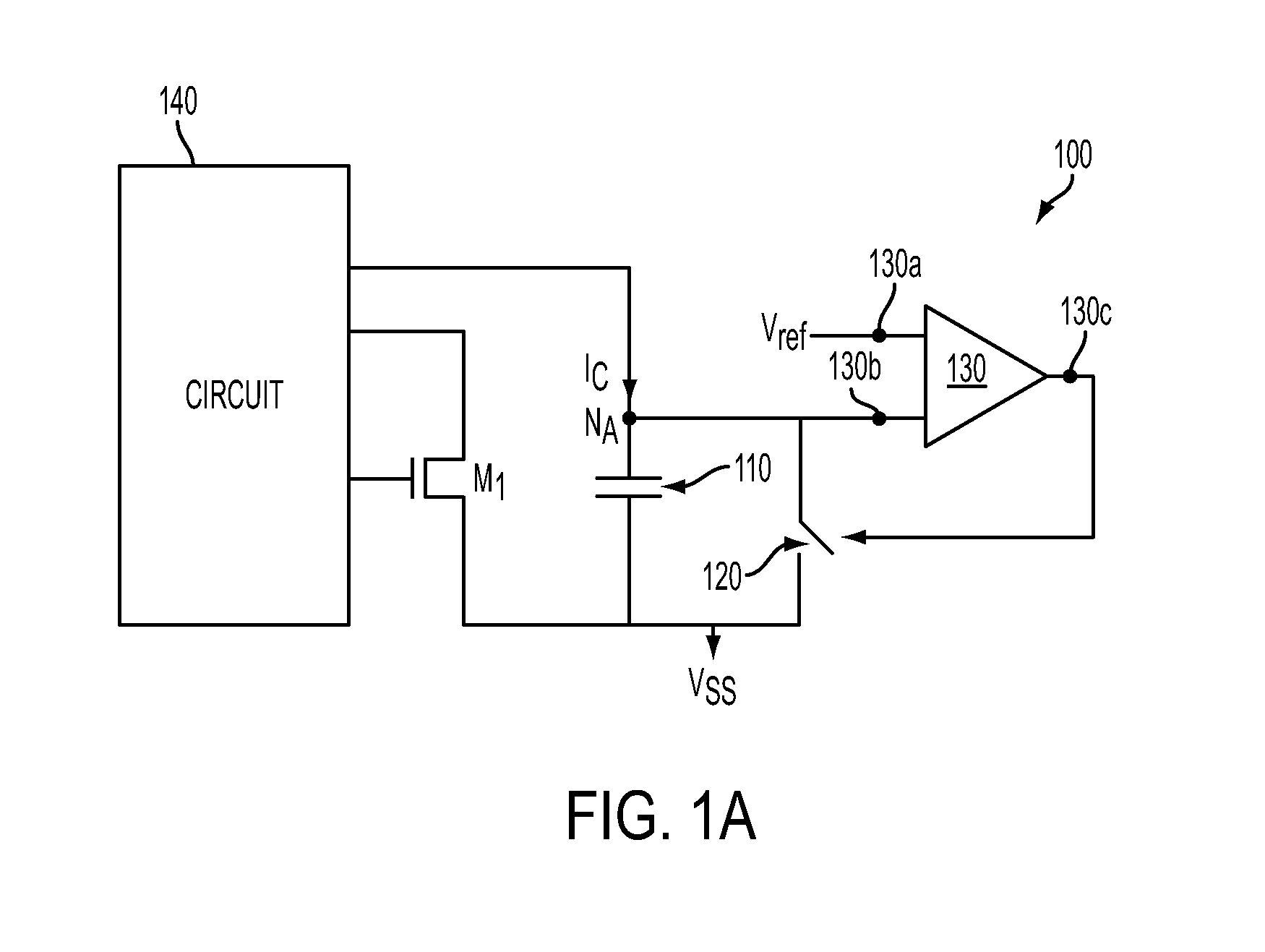
The present disclosure relates generally to the field of semiconductor circuits, and more particularly, to integrated circuits for providing clock periods and operating methods thereof. Memory circuits have been used in various applications. Conventionally, a dynamic random access memory (DRAM) circuit includes a plurality of memory cells. For a conventional DRAM circuit in which arrays of capacitive storage memory cells are provided, each memory cell has an access transistor. Data stored in such memory cells is actually a charge stored on a small capacitor. When the data are to be output, the access transistor is activated by a word line (WL) that is electrically coupled to the gate or control terminal of the transistor. The access transistor can couple the capacitor to a bit line (BL) coupled to a sense amplifier for sensing the voltage of the capacitor. The present disclosure is best understood from the following detailed description when read with the accompanying figures. It is emphasized that, in accordance with the standard practice in the industry, various features are not drawn to scale and are used for illustration purposes only. In fact, the numbers and dimensions of the various features may be arbitrarily increased or reduced for clarity of discussion. Data stored in memory cells of the DRAM circuit are vulnerable because of charge leakages of the memory cells. To retain the data stored in the DRAM circuit, a refresh operation is periodically applied to the DRAM circuit to recharge capacitors of the memory cells. Generally, a temperature-controlled oscillator (TCO) has been used to provide a refresh period or refresh frequency for the refresh operation. The TCO has a capacitor electrically coupled with a switch. A fixed current is provided to charge the capacitor. A comparator compares a voltage level on a top plate of the capacitor and a reference voltage that is inversely proportional to absolute temperature. If the voltage level is higher than the reference voltage, the switch is closed such that charges stored in the capacitor can be discharged and the voltage level on the top plate of the capacitor declines. If the voltage level is lower than the reference voltage, the switch is opened such that the capacitor can be charged by the fixed current and the voltage level on the top plate of the capacitor increases. By detecting the open-close state of the switch, the refresh period or the refresh frequency is provided. It is found that the environmental temperature around the DRAM circuit affects the charge leakages. If the environmental temperature increases, the charge leakages of the memory cell capacitors also increase. The refresh period should be shortened and the refresh frequency should be increased to refresh the memory cells. If the environmental temperature decreases, the charge leakages of the memory cell capacitors are decreased. The refresh frequency can be slowed down. It is proposed that the refresh frequency at 125° C. should be about six times the refresh frequency at 25° C. It is understood that the following disclosure provides many different embodiments, or examples, for implementing different features of the disclosure. Specific examples of components and arrangements are described below to simplify the present disclosure. These are, of course, merely examples and are not intended to be limiting. In addition, the present disclosure may repeat reference numerals and/or letters in the various examples. This repetition is for the purpose of simplicity and clarity and does not in itself dictate a relationship between the various embodiments and/or configurations discussed. Moreover, the formation of a feature on, connected to, and/or coupled with or to another feature in the present disclosure that follows may include embodiments in which the features are formed in direct contact, and may also include embodiments in which additional features may be formed interposing the features, such that the features may not be in direct contact. In addition, spatially relative terms, for example, “lower,” “upper,” “horizontal,” “vertical,” “above,” “below,” “up,” “down,” “top,” “bottom,” etc. as well as derivatives thereof (e.g., “horizontally,” “downwardly,” “upwardly,” etc.) are used for ease of the present disclosure of one features relationship to another feature. The spatially relative terms are intended to cover different orientations of the device including the features. Referring to Referring to As noted, the reference voltage Vrefcan be temperature independent. The term “temperature independent” here means that the reference voltage Vrefis substantially free from being affected by the environmental temperature. The circuit 140 can be configured to provide a bias voltage Vbiasto the gate of the transistor M1so as to control the current IC. In some embodiments, the bias voltage Vbiasis programmable and temperature dependent. The term “programmable” here means that the bias voltage Vbiascan be adjusted by adjusting at least one parameter, such as one or more impedances and/or resistances of at least one component within the circuit 140, and/or a proportional factor. By adjusting the bias voltage Vbias, the current ICcan be adjusted in correspondence to a change of environmental temperature around the circuit 100. In some embodiments, if the environmental temperature goes up, the bias voltage Vbiasis raised to increase the current ICfor charging the capacitor 110. Because a large current is provided to charge the capacitor 110, the clock period for refreshing memory cells can be thus reduced. In other embodiments, if the environmental temperature goes down, the bias voltage Vbiasis lowered to decrease the current ICfor charging the capacitor 110. Because a small current is provided to charge the capacitor 110, the clock period for refreshing memory cells can be increased. In still other embodiments, the circuit 100 can provide a refresh frequency at 125° C. that can be about six times the refresh frequency at 25° C. In some embodiments, the transconductance amplifier 141 can include a current mirror 201 and a pair of transistors 203 and 205 as shown in Referring again to In some embodiments, the input node 145 As noted, the bias voltage Vbiascan be programmable. In some embodiments, the bias voltage Vbiascan be adjusted by adjusting the resistances RAand RB. The resistances RAand/or RBcan be adjustable to achieve a desired bias voltage Vbias. In some embodiments, the bias voltage Vbiascan be represented below in Equation (1) wherein the reference voltage Vrefis temperature independent, VEBis temperature dependent, and the resistances RAand RBcan each be fixed or adjustable. From Equation (1), the bias voltage Vbiascan be adjusted by adjusting the ratio RB/RA. In some embodiments, the environmental temperature around the integrated circuit 100 rises. If the environmental temperature increases, charge leakages of memory cells are increased. To retain data stored in the memory cells, the clock period should be shortened or the clock frequency should be increased. In this embodiment, the Step 310 can include increasing the bias voltage Vbiasto turn up the transistor M1so as to induce increasing the current IC. For example, the increased bias voltage Vbiascan turn up the transistor M1as shown in The method 300 can include comparing the temperature-independent reference voltage Vrefand the voltage level on the node NAof the capacitor 110 for controlling an open/close state of the switch 120 so as to generate the clock period (Step 320). If the voltage level on the node NAis higher than the reference voltage Vref, the comparator 130 can output a signal, closing the switch 120, such that charges stored in the capacitor 110 can be discharged. If the voltage level on the node NAis lower than the reference voltage Vref, the comparator 130 can output a signal, opening the switch 120, such that the current ICcan be supplied to charge the capacitor 110. By detecting the close/open state of the switch 120, a clock period that is provided for refreshing memory cells can be generated. In some embodiments, a clock period (T) for refreshing memory cells can be represented below in Equation (2) wherein, Cxrepresents the capacitance of the capacitor 110. As noted, the clock period T is inversely proportional to the current IC. The reference voltage Vrefis temperature independent. In some embodiments, the reference voltage Vrefand the capacitance Cxcan be fixed factors. If the environmental temperature rises such that the current ICis increased, the clock period T can be reduced and the clock frequency can be increased. In some embodiments, the environmental temperature around the integrated circuit 100 goes down. If the environmental temperature falls, charge leakages of memory cells may become small. To retain data stored in the memory cells, the clock period can be extended or the clock frequency can be slowed down. In this embodiment, the Step 310 can include decreasing the bias voltage Vbiasto turn down the transistor M1so as to decrease the current IC. For example, the decreased bias voltage Vbiascan turn down the transistor M1as shown in Referring to Referring to In some embodiments, the temperature-dependent reference voltage Vref′ is programmable. The term “programmable” here means that the reference voltage Vref′ can be adjusted by adjusting one or more proportional factors and/or one or more impedances and/or resistances of at least one component of the circuit 440. In other embodiments, the temperature-dependent current IC′ is programmable. The term “programmable” here means that the temperature-dependent current IC′ can be adjusted by adjusting one or more proportional factors and/or one or more impedances and/or resistances of at least one component of the circuit 450. By adjusting the temperature-dependent reference voltage Vref′ and/or the temperature-dependent current IC′, the clock period T′ can be modified. As noted, the temperature-dependent reference voltage Vref′ and/or the temperature-dependent current IC′ can be adjusted in correspondence to a change of environmental temperature around the circuit 400. In some embodiments, if the environmental temperature rises, the temperature-dependent reference voltage Vref′ can be reduced and/or the temperature-dependent current IC′ can be increased. By adjusting the temperature-dependent reference voltage Vref′ and/or the temperature-dependent current IC′, the clock frequency for refreshing memory cells can be increased. In other embodiments, if the environmental temperature falls, the temperature-dependent reference voltage Vref′ can be increased and/or the temperature-dependent current IC′ can be reduced. By adjusting the temperature-dependent reference voltage Vref′ and/or the temperature-dependent current IC′, the clock frequency for refreshing memory cells can be reduced. Referring to Referring to Referring again to Referring again to In some embodiments, the current mirror 451 can be electrically coupled with the input node 430 Referring to Referring again to In some embodiments for providing the temperature-dependent reference voltage Vref′, the current minor 445 (shown in In some embodiments, a circuit 700 of the bandgap reference circuit 460 that is configured to provide the temperature-independent current Ibgcan include a current minor 710, a resistor 720, and a bipolar transistor 730 as shown in In some embodiments, the current mirror 710 can provide temperature-dependent currents Iaand Ibtoward the nodes X and Y, respectively. The temperature-dependent currents Iacan be substantially equal to or proportional to the temperature-dependent current Ib. In other embodiments, the temperature-dependent currents Iaand Ibboth are proportional to absolute temperature (PTAT) currents. In still other embodiments, the temperature-independent current Ibgcan be represented as below in Equation (3) wherein, RXrepresents a resistance of the resistor 720, and VEB′ represents a voltage across the emitter and base of the bipolar transistor 730. The temperature-dependent voltage VEB′ can be inversely proportional to absolute temperature. Since the temperature-dependent current Iais proportional to absolute temperature, the temperature effects of the temperature-dependent voltage VEB′ and the temperature-dependent current Iacan be substantially canceled by each other. The current Ibgis thus temperature independent. Referring again to Referring to wherein RB′ is the resistance of the resistor R2′ and KVEB′ is inversely proportional to absolute temperature. The current is temperature dependent. Since the current and the temperature-independent current IC1′ are provided to the current minor 443, the current mirror 441 can provide the resistor R1′ a current Iref′ that is temperature dependent and can be represented below as in Equation (4). Since the current Iref′ flows through the resistor R1′, the temperature-dependent voltage Vref′ on the input node 430 As noted, the temperature-dependent voltage Vref′ can be programmable. In some embodiments, the temperature-dependent voltage Vref′ can be programmed by adjusting at least one of the resistances RA′, RB′, the proportional factor K, and the temperature-independent current IC1′. In some embodiments for providing the temperature-dependent current IC′, the current mirror 455 (shown in wherein RC′ represents the resistance of the resistor R3′. The current mirror 455 can minor the temperature-dependent current to the current mirror 453. In some embodiments, the current minor 453 can receive a temperature-independent current IC2′. In other embodiments, the temperature-independent current IC2′ can be provided from the circuit 440 or the current minor 445. Since the temperature-dependent current and the temperature-independent current IC2′ are provided to the current minor 453, the current mirror 451 can provide the temperature-dependent current IC′ that can be represented below in Equation (6). As noted, the temperature-dependent current IC′ can be programmable. In some embodiments, the temperature-dependent current IC′ can be programmed by adjusting the resistance RC′ and/or the temperature-independent current IC2′. In some embodiments, the environmental temperature around the integrated circuit 400 rises. If the environmental temperature increases, charge leakages of memory cells are increased. To retain data stored in the memory cells, the clock period should be shortened or the clock frequency should be increased. In this embodiment, the method 600 can include increasing the temperature-dependent current IC′ and/or decreasing the temperature-dependent reference voltage Vref′. The method 600 can include comparing the temperature-dependent reference voltage Vref′ and the voltage level on the node NA′ of the capacitor 410 ( In some embodiments, a clock period (T′) for refreshing memory cells can be represented below in Equation (7) wherein, Cx′ represents the capacitance of the capacitor 410 and can be fixed. As noted, the clock period T′ is inversely proportional to the current IC′. If the environment temperature rises, the temperature-dependent current IC′ can be increased and/or the temperature-dependent reference voltage Vref′ can be decreased. Based on Equation (7), the clock period T′ can be reduced and the refresh frequency can be increased. In some embodiments, the environmental temperature around the integrated circuit 400 goes down. If the environmental temperature falls, charge leakages of memory cells become small. To retain data stored in the memory cells, the clock period can be longer or the clock frequency can be slowed down. In this embodiment, the method 600 can include decreasing the temperature-dependent current IC′ and/or increasing the temperature-dependent reference voltage Vref′. Based on Equation (7), the clock period T′ can be proportionally increased and the clock frequency is decreased. In some embodiments, the processor 810 and the memory circuit 801 can be formed within a system that can be physically and electrically coupled with a printed wiring board or printed circuit board (PCB) to form an electronic assembly. The electronic assembly can be part of an electronic system such as computers, wireless communication devices, computer-related peripherals, entertainment devices, or the like. In some embodiments, the system 800 including the memory circuit 801 can provide an entire system in one IC, so-called system on a chip (SOC) or system on integrated circuit (SOIC) devices. These SOC devices may provide, for example, all of the circuitry needed to implement a cell phone, personal data assistant (PDA), digital VCR, digital camcorder, digital camera, MP3 player, or the like in a single integrated circuit. The foregoing outlines features of several embodiments so that those skilled in the art may better understand the aspects of the present disclosure. Those skilled in the art should appreciate that they may readily use the present disclosure as a basis for designing or modifying other processes and structures for carrying out the same purposes and/or achieving the same advantages of the embodiments introduced herein. Those skilled in the art should also realize that such equivalent constructions do not depart from the spirit and scope of the present disclosure, and that they may make various changes, substitutions, and alterations herein without departing from the spirit and scope of the present disclosure. An integrated circuit includes a capacitor. A switch is electrically coupled with the capacitor in a parallel fashion. A comparator includes a first input node, a second input node, and an output node. The second input node is electrically coupled with a first plate of the capacitor. The output node is electrically coupled with the switch. A transistor is electrically coupled with a second plate of the capacitor. A circuit is electrically coupled with a gate of the transistor. The circuit is configured to provide a bias voltage to the gate of the transistor so as to control a current that is supplied to charge the capacitor. 1. An integrated circuit for providing a clock period, the integrated circuit comprising:
a capacitor; a switch electrically coupled with the capacitor in a parallel fashion; a comparator including a first input node, a second input node, and a first output node, the second input node being electrically coupled with a first plate of the capacitor, the output node being electrically coupled with the switch; a transistor electrically coupled with a second plate of the capacitor; and a circuit electrically coupled with a gate of the transistor, the circuit being configured to provide a bias voltage to the gate of the transistor so as to control a current that is supplied to charge the capacitor. 2. The integrated circuit of a transconductance amplifier electrically coupled with the transistor and the capacitor; an amplifier including a third input node, a fourth input node, and a second output node, wherein the third input node is electrically coupled with the transconductance amplifier; a first resistor electrically coupled with the fourth input node; and a second resistor electrically coupled between the fourth input node and the second output node. 3. The integrated circuit of 4. The integrated circuit of 5. The integrated circuit of 6. The integrated circuit of the circuit is configured to increase the bias voltage to increase the current flowing through the transistor and a clock period that is inversely proportional to the current is decreased, if an environmental temperature around the integrated circuit is increased, and if the environmental temperature around the integrated circuit is decreased, the circuit is configured to increase the bias voltage to turn down the transistor such that the current is decreased and the clock period that is inversely proportional to the current is increased. 7. The integrated circuit of 8. An integrated circuit for providing a clock period, the integrated circuit comprising:
a capacitor; a switch coupled with the capacitor in a parallel fashion; a comparator including a first input node, a second input node, and a first output node, the second input node being electrically coupled with the capacitor, the first output node being electrically coupled with the switch; a first circuit electrically coupled with the first input node of the comparator, the first circuit being configured to provide a temperature-dependent reference voltage; and a second circuit electrically coupled with the capacitor, the second circuit being configured to provide a first temperature-dependent current that is supplied to charge the capacitor, wherein the temperature-dependent reference voltage and the first temperature-dependent current are programmable, and at least one of the temperature-dependent reference voltage and the first temperature-dependent current is adjusted so as to adjust a clock period for refreshing memory cells that are electrically coupled with the integrated circuit. 9. The integrated circuit of a first resistor electrically coupled with the first input node of the comparator; a first current mirror electrically coupled with the first input node of the comparator; a second current mirror electrically coupled with the first current mirror; a third current mirror electrically coupled with the second current mirror; a fourth current minor electrically coupled with the second current minor; a second resistor electrically coupled between the fourth current mirror and a power line that is configured to provide a power voltage; and a first amplifier including a third input node, a fourth input node, and a second output node, wherein the third input node of the first amplifier is configured to receive a first temperature-dependent voltage, the fourth input node of the first amplifier is electrically coupled with a node between the second resistor and the fourth current minor, and the second output node of the first amplifier is electrically coupled with the fourth current mirror. 10. The integrated circuit of and wherein the temperature-dependent reference voltage (Vref′) is represented by following equation: 11. The integrated circuit of 12. The integrated circuit of a fifth current minor electrically coupled with the second input node of the comparator; a sixth current mirror electrically coupled with the fifth current mirror; a seventh current mirror electrically coupled with the sixth current minor; a third resistor electrically coupled between the seventh current mirror and a power line that is configured to provide a power voltage; and a second amplifier including a fifth input node, a sixth input node, and a third output node, wherein the fifth input node of the second amplifier is configured to receive a second temperature-dependent voltage, the sixth input node of the second amplifier is electrically coupled with a node between the third resistor and the seventh current minor, and the second output node of the first amplifier is electrically coupled with the seventh current mirror. 13. The integrated circuit of the sixth current mirror is configured to receive a second temperature-independent current (IC2′) from the first circuit, and the first temperature-dependent current (IC′) is represented by following equation: 14. The integrated circuit of 15. The integrated circuit of if an environmental temperature around the integrated circuit is increased, the first circuit is configured to decrease the temperature-dependent reference voltage and/or the second circuit is configured to increase the first temperature-dependent current; and if the environmental temperature around the integrated circuit is decreased, the first circuit is configured to increase the temperature-dependent reference voltage and/or the second circuit is configured to decrease the first temperature-dependent current. 16. A method of operating an integrated circuit for generating a clock period for refreshing memory cells of a memory circuit, the integrated circuit including a capacitor, a switch, a comparator, and a transistor, the switch being electrically coupled with the capacitor in a parallel fashion, the comparator being electrically coupled with the switch and the capacitor, the transistor being electrically coupled with the capacitor, the method comprising:
providing a bias voltage to a gate of the transistor so as to control a current that is supplied to charge the capacitor; and comparing a temperature-independent reference voltage received by the comparator and a voltage level on a node of the capacitor for controlling an open/close state of the switch so as to generate the clock period. 17. The method of a transconductance amplifier electrically coupled with the transistor and the capacitor; an amplifier electrically coupled with the transconductance amplifier; a first resistor electrically coupled with an input node of the amplifier; and a second resistor electrically coupled between the input node and an output node of the amplifier. 18. The method of 19. The method of 20. The method of the bias voltage is increased to turn up the transistor such that the current is increased and a clock period that is inversely proportional to the current is decreased, if an environmental temperature around the integrated circuit is increased; and the bias voltage is decreased to turn down the transistor such that the current is decreased and the clock period that is inversely proportional to the current is increased, if the environmental temperature around the integrated circuit is decreased. TECHNICAL FIELD
BACKGROUND
BRIEF DESCRIPTION OF THE DRAWINGS
DETAILED DESCRIPTION OF THE DISCLOSURE