III-NITRIDE SEMICONDUCTOR LASER DEVICE, AND METHOD OF FABRICATING THE III- NITRIDE SEMICONDUCTOR LASER DEVICE
1. Field of the Invention The present invention relates to a group-III nitride semiconductor laser device, and a method of fabricating the group-III nitride semiconductor laser device. 2. Related Background Art Non Patent Literature 1 discloses a laser diode made on an m-plane GaN substrate. The laser diode has two cleaved end faces for an optical cavity. One of the cleaved end faces is a +c plane and the other cleaved end faces is a −c plane. In this laser diode, the reflectance of a dielectric multilayer film on the front end face (emitting face) is 70% and the reflectance of a dielectric multilayer film on the rear end face is 99%. Non Patent Literature 2 discloses a laser diode made on a GaN substrate inclined at the angle of 1 degree with respect to the m-plane to the −c axis direction. The laser diode has two cleaved end faces for an optical cavity. One cleaved end face is a +c plane and the other cleaved end face is a −c plane. In this laser diode, the reflectance of the dielectric multilayer film on the front end face (exit face) is 90% and the reflectance of the dielectric multilayer film on the rear end face is 95%.
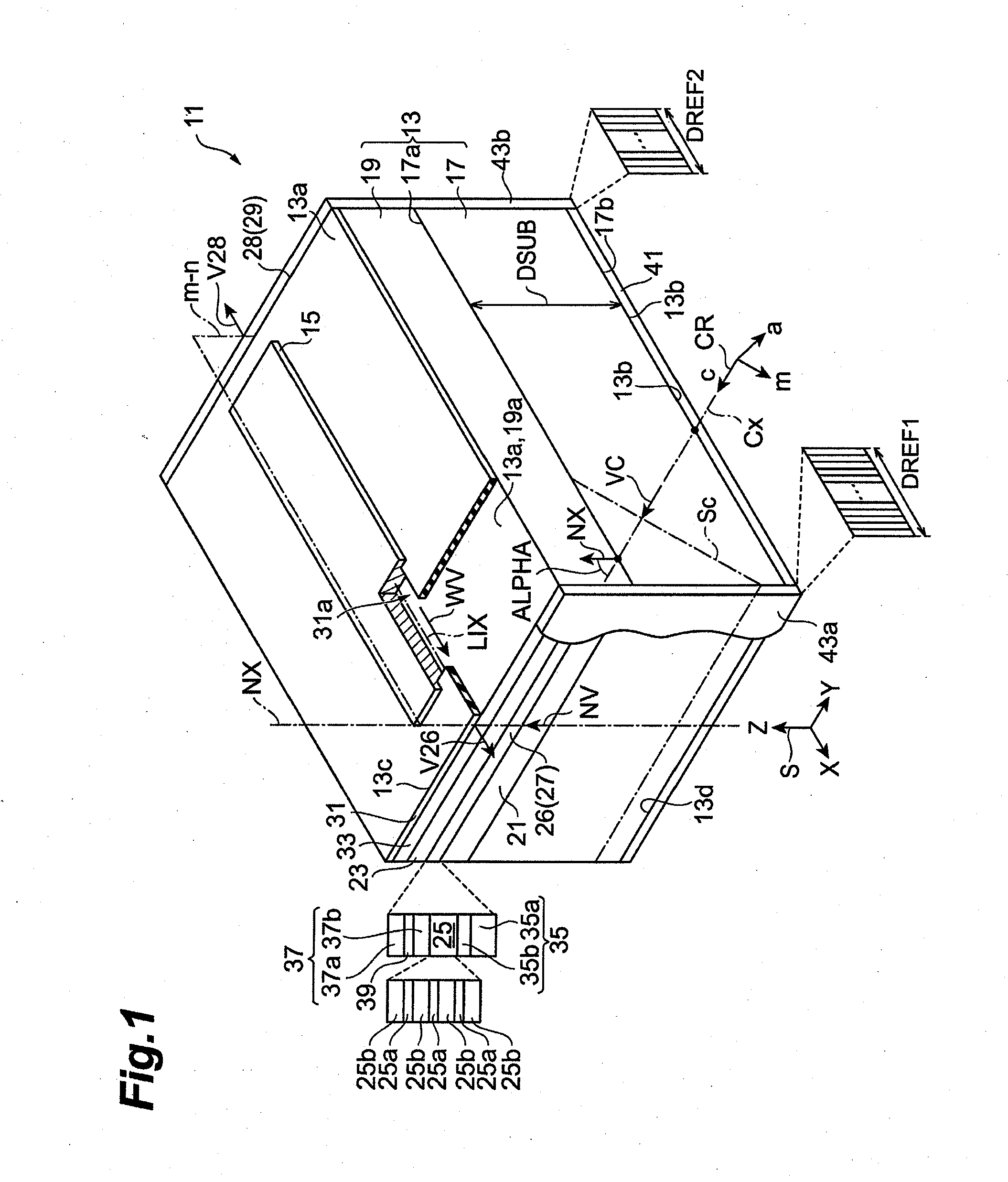
A light emitting device is made on a semipolar surface of a GaN substrate. In the GaN surface having semipolar nature, the c-axis of GaN is inclined with respect to a normal to the semipolar surface of the GaN substrate. In fabrication of a semiconductor laser using the GaN semipolar surface, when the c-axis of GaN is inclined toward an extending direction of a waveguide of the semiconductor laser, it becomes feasible to form the end faces available for an optical cavity. Dielectric multilayer films with desired reflectances are formed on these respective end faces to form the optical cavity. The thicknesses of the dielectric multilayer films on the two end faces are different from each other in order to obtain the dielectric multilayer films with the mutually different reflectances. Since a laser beam is emitted from the front end face, the reflectance of the dielectric multilayer film on the front end face is set smaller than that of the dielectric multilayer film on the rear end face. It is found by Inventors' experiments that when some semiconductor lasers are fabricated as described above, these semiconductor lasers have various device lifetimes and we do not have any clear reasons for the long device lifetimes and short device lifetimes. The Inventors conduct research on this point and come to find that the difference in the device lifetime is associated with crystal orientations of the semiconductor end faces for the optical cavity and the thicknesses of the dielectric multilayer films formed thereon. It is an object of the present invention to provide a III-nitride semiconductor laser device with a long device lifetime. It is another object of the present invention to provide a method of fabricating a III-nitride semiconductor laser device with a long device lifetime. A III-nitride semiconductor laser device according to a first aspect of the present invention comprises: (a) a laser structure comprising a support base and a semiconductor region, the support base having a semipolar primary surface of a III-nitride semiconductor, and the semiconductor region being provided on the semipolar primary surface of the support base; and (b) first and second dielectric multilayer films for an optical cavity of the nitride semiconductor laser device, the first and second dielectric multilayer films being provided on first and second end faces of the semiconductor region, respectively, the semiconductor region including a first cladding layer of a first conductivity type gallium nitride-based semiconductor, a second cladding layer of a second conductivity type gallium nitride-based semiconductor, and an active layer, and the an active layer being provided between the first cladding layer and the second cladding layer, the first cladding layer, the second cladding layer, and the active layer being arranged in a normal axis to the semipolar primary surface, the active layer comprising a gallium nitride-based semiconductor layer, a c+ axis vector being inclined at an angle in a range of not less than 45 degrees and not more than 80 degrees and of not less than 100 degrees and not more than 135 degrees toward a direction of any one crystal axis of m- and a-axes of the III-nitride semiconductor with respect to a normal vector, the c+ axis vector indicating a direction of a <0001> axis of the III-nitride semiconductor of the support base, and the normal vector indicating a direction of the normal axis, the first and second end faces intersecting with a reference plane, the reference plane being defined by the normal axis and the one crystal axis of the hexagonal III-nitride semiconductor, the c+ axis vector making an acute angle with a waveguide vector, and the waveguide vector indicating a direction from the second end face to the first end face, and a thickness of the second dielectric multilayer film being smaller than a thickness of the first dielectric multilayer film. In this III-nitride semiconductor laser device, the c+ axis vector makes the acute angle with the waveguide vector and this waveguide vector is directed in the direction from the second end face to the first end face. An angle between the c+ axis vector and a vector normal to the second end face is larger than an angle between the c+ axis vector and a vector normal to the first end face. In this laser device, since the thickness of the second dielectric multilayer film on the second end face is smaller than the thickness of the first dielectric multilayer film on the first end face, the second dielectric multilayer film on the second end face works as the front side and a laser beam is emitted from this front side. The first dielectric multilayer film on the first end face works as the rear side and most of the laser beam is reflected by this rear side. In the laser device on the semipolar plane, when the thickness of the second dielectric multilayer film on the front side is smaller than the thickness of the first dielectric multilayer film on the rear side, reduction is achieved in device degradation due to the dielectric multilayer film on the end face, so as to avoid reduction in device lifetime. The III-nitride semiconductor laser device according to the first aspect of the present invention can be configured as follows: the semiconductor region is located between the first surface and the support base, and wherein each of the first and second end faces is included in a fractured face, and the fractured face extends from an edge of the first surface to an edge of the second surface. Since in the III-nitride semiconductor laser device the first and second end faces of the laser structure intersect with the reference plane defined by the normal axis to the primary surface and the a-axis or m-axis of the hexagonal III-nitride semiconductor, the first and second end faces can be formed as fractured faces, and each of the fractured faces extends from the edge of the first surface to the edge of the second surface. The III-nitride semiconductor laser device according to the first aspect of the present invention can be configured so that the c-axis of the III-nitride semiconductor is inclined toward the direction of the m-axis of the nitride semiconductor. In another embodiment, the III-nitride semiconductor laser device according to the first aspect of the present invention can be configured so that the c-axis of the III-nitride semiconductor is inclined toward the direction of the a-axis of the nitride semiconductor. The III-nitride semiconductor laser device according to the first aspect of the present invention can be configured so that the primary surface of the support base is inclined in the range of not less than −4 degrees and not more than +4 degrees with respect to any one of {10-11}, {20-21}, {20-2-1}, and {10-1-1} planes. Furthermore, the III-nitride semiconductor laser device according to the first aspect of the present invention can be configured so that the primary surface of the support base is any one of the {10-11} plane, {20-21} plane, {20-2-1} plane, and {10-1-1} plane. In this III-nitride semiconductor laser device, when the c-axis of the III-nitride semiconductor is inclined toward the direction of the m-axis of the nitride semiconductor, practical plane orientations and angular range for the primary surface can include at least the aforementioned plane orientations and angle range. The III-nitride semiconductor laser device according to the first aspect of the present invention can be configured so that the primary surface of the support base is inclined in the range of not less than −4 degrees and not more than +4 degrees from any one of {11-22}, {11-21}, {11-2-1}, and {11-2-2} planes. Furthermore, the III-nitride semiconductor laser device according to the first aspect of the present invention can be configured so that the primary surface of the support base is any one of the {11-22} plane, {11-21} plane, {11-2-1} plane, and {11-2-2} plane. In this III-nitride semiconductor laser device, when the c-axis of the III-nitride semiconductor is inclined toward the direction of the a-axis of the nitride semiconductor, practical plane orientations and angular range for the primary surface can encompass at least the aforementioned plane orientations and angle range. The III-nitride semiconductor laser device according to the first aspect of the present invention can be configured so that the active layer comprises a well layer comprised of a strained gallium nitride-based semiconductor containing indium as a constituent element. Furthermore, the III-nitride semiconductor laser device according to the first aspect of the present invention can be configured so that the active layer comprises a well layer comprised of strained InGaN. With this III-nitride semiconductor laser device, the degradation of interest is observed in the GaN-based semiconductor containing indium as a Group III constituent element. The degree of degradation becomes more prominent with increase in the indium composition. The III-nitride semiconductor laser device according to the first aspect of the present invention can be configured so that the active layer is adapted to generate light at a wavelength of 430 to 550 nm. This III-nitride semiconductor laser device can provide the light in the aforementioned wavelength range by use of the well layer that comprises the strained GaN-based semiconductor containing, for example, indium as a Group III constituent element. The III-nitride semiconductor laser device according to the first aspect of the present invention can be configured so that the III-nitride semiconductor is GaN. With this III-nitride semiconductor laser device, for example, the emission of light in the aforementioned wavelength range (wavelength range from blue to green) can be provided by creation of the laser structure using the GaN primary surface. In the III-nitride semiconductor laser device according to the first aspect of the present invention, the first dielectric multilayer film has a dielectric layer, and the dielectric layer in the first dielectric multilayer film is comprised of at least one of silicon oxide, silicon nitride, silicon oxynitride, titanium oxide, titanium nitride, titanium oxynitride, zirconium oxide, zirconium nitride, zirconium oxynitride, zirconium fluoride, tantalum oxide, tantalum nitride, tantalum oxynitride, hafnium oxide, hafnium nitride, hafnium oxynitride, hafnium fluoride, aluminum oxide, aluminum nitride, aluminum oxynitride, magnesium fluoride, magnesium oxide, magnesium nitride, magnesium oxynitride, calcium fluoride, barium fluoride, cerium fluoride, antimony oxide, bismuth oxide, and gadolinium oxide. The second dielectric multilayer film has a dielectric layer, and the dielectric layer in the second dielectric multilayer film is comprised of at least one of silicon oxide, silicon nitride, silicon oxynitride, titanium oxide, titanium nitride, titanium oxynitride, zirconium oxide, zirconium nitride, zirconium oxynitride, zirconium fluoride, tantalum oxide, tantalum nitride, tantalum oxynitride, hafnium oxide, hafnium nitride, hafnium oxynitride, hafnium fluoride, aluminum oxide, aluminum nitride, aluminum oxynitride, magnesium fluoride, magnesium oxide, magnesium nitride, magnesium oxynitride, calcium fluoride, barium fluoride, cerium fluoride, antimony oxide, bismuth oxide, and gadolinium oxide. In this III-nitride semiconductor laser device, practical materials of the dielectric films can include silicon oxide (e.g., SiO2), silicon nitride (e.g., Si3N4), silicon oxynitride (e.g., SiOxN1-x), titanium oxide (e.g., TiO2), titanium nitride (e.g., TiN), titanium oxynitride (e.g., TiOxN1-x), zirconium oxide (e.g., ZrO2), zirconium nitride (e.g., ZrN), zirconium oxynitride (e.g., ZrOxN1-x), zirconium fluoride (e.g., ZrF4), tantalum oxide (e.g., Ta2O5), tantalum nitride (e.g., Ta3N5), tantalum oxynitride (e.g., TaOxN1-x), hafnium oxide (e.g., HfO2), hafnium nitride (e.g., HfN), hafnium oxynitride (e.g., HfOxN1-x), hafnium fluoride (e.g., HfF4), aluminum oxide (e.g., Al2O3), aluminum nitride (e.g., AlN), aluminum oxynitride (e.g., AlOxN1-x), magnesium fluoride (e.g., MgF2), magnesium oxide (e.g., MgO), magnesium nitride (e.g., Mg3N2), magnesium oxynitride (e.g., MgOxN1-x), calcium fluoride (e.g., CO2), barium fluoride (e.g., BaF2), cerium fluoride (e.g., CeF3), antimony oxide (e.g., Sb2O3), bismuth oxide (e.g., Bi2O3), and gadolinium oxide (e.g., Gd2O3). A second aspect of the present invention relates to a method of fabricating a III-nitride semiconductor laser device. This method comprises the steps of: (a) preparing a substrate with a semipolar primary surface, the semipolar primary surface comprising a hexagonal III-nitride semiconductor; (b) forming a substrate product having a laser structure, an anode electrode, and a cathode electrode, the laser structure comprising a substrate and a semiconductor region, and the semiconductor region being formed on the semipolar primary surface; (c) after forming the substrate product, forming first and second end faces; and (d) forming first and second dielectric multilayer films for an optical cavity of the nitride semiconductor laser device on the first and second end faces, respectively, the first and second end faces intersecting with a reference plane, the reference plane being defined by a normal axis to the semipolar primary surface and any one crystal axis of a- and m-axes of the hexagonal III-nitride semiconductor, the semiconductor region comprising a first cladding layer of a first conductivity type gallium nitride-based semiconductor, a second cladding layer of a second conductivity type gallium nitride-based semiconductor, and an active layer, and the active layer being provided between the first cladding layer and the second cladding layer, the first cladding layer, the second cladding layer, and the active layer being arranged in a direction of the normal axis, the active layer comprising a gallium nitride-based semiconductor layer, the semipolar primary surface of the substrate being inclined at an angle in a range of not less than 45 degrees and not more than 80 degrees and of not less than 100 degrees and not more than 135 degrees with respect to a plane perpendicular to a c+ axis vector, and the c+ axis vector indicating a direction of the <0001> axis of the nitride semiconductor, the c+ axis vector making an acute angle with a waveguide vector, and the waveguide vector indicating a direction from the second end face to the first end face, and a thickness of the second dielectric multilayer film being smaller than a thickness of the first dielectric multilayer film. According to this method, the waveguide vector making the acute angle with the c+ axis vector corresponds to the direction from the second end face to the first end face and the second dielectric multilayer film (C− side) on the second end face is formed so as to be thinner than the first dielectric multilayer film (C+ side) on the first end face in thickness; therefore, it is feasible to reduce the device degradation with deterioration of crystal quality proceeding from the second end face due to the dielectric multilayer film on the end face, and thereby avoiding the reduction in device lifetime. In this III-nitride semiconductor laser device, the angle between the c+ axis vector and the normal vector to the second end face is larger than the angle between the c+ axis vector and the normal vector to the first end face. When the thickness of the second dielectric multilayer film (C− side) on the front side is smaller than the thickness of the first dielectric multilayer film (C+ side) on the rear side, the second dielectric multilayer film on the second end face works as the front side and a laser beam is emitted from this front side. The first dielectric multilayer film on the first end face works as the rear side and most of the laser beam is reflected by this rear side. The method according to the second aspect of the present invention further comprises the step of, prior to forming the first and second dielectric multilayer films, determining plane orientations of the first and second end faces. This method allows the selection of the appropriate dielectric multilayer films for the respective end faces in accordance with the result of determination and allows the growth of the dielectric multilayer films on the respective end faces. The method according to the second aspect of the present invention can be configured as follows: the step of forming the first and second end faces comprises: the step of forming the first and second end faces comprises the steps of scribing a first surface of the substrate product; and breaking the substrate product by press against a second surface of the substrate product to form a laser bar having the first and second end faces, the first and second end faces of the laser bar being formed by the breaking, the first surface being opposite to the second surface, the semiconductor region being provided between the first surface and the substrate, and each of the first and second end faces of the laser bar being included in a fractured face, and the fractured face extending from the first surface to the second surface and being formed by the breaking. In this method, since the first and second end faces of the laser bar intersect with the reference plane defined by the normal axis to the primary surface and the a-axis or m-axis of the hexagonal III-nitride semiconductor, the first and second end faces can be formed as fractured faces by the scribe formation and press, and the fractured faces each extend from an edge of the first surface to an edge of the second surface. The method according to the second aspect of the present invention can be configured so that the c-axis of the III-nitride semiconductor is inclined toward the direction of the m-axis of the nitride semiconductor. In another embodiment, the method according to the second aspect of the present invention can be configured so that the c-axis of the III-nitride semiconductor is inclined toward the direction of the a-axis of the nitride semiconductor. The method according to the second aspect of the present invention can be configured so that the primary surface of the substrate is inclined in a range of not less than −4 degrees and not more than +4 degrees with respect to any one of {10-11}, {20-21}, {20-2-1}, and {10-1-1} planes. Furthermore, the method according to the second aspect of the present invention can be configured so that the primary surface of the substrate is any one of the {10-11} plane, {20-21} plane, {20-2-1} plane, and {10-1-1} plane. In this method, when the c-axis of the III-nitride semiconductor is inclined toward the direction of the m-axis of the nitride semiconductor, practical plane orientations and angular range for the primary surface include at least the aforementioned plane orientations and angle range. The method according to the second aspect of the present invention can be configured so that the primary surface of the substrate is inclined in the range of not less than −4 degrees and not more than +4 degrees from any one of {11-22}, {11-21}, {11-2-1}, and {11-2-2} planes. Furthermore, the method according to the second aspect of the present invention can be configured so that the primary surface of the substrate is any one of the {11-22} plane, {11-21} plane, {11-2-1} plane, and {11-2-2} plane. In this substrate, when the c-axis of the III-nitride semiconductor is inclined toward the direction of the a-axis of the nitride semiconductor, practical plane orientations and angular range for the primary surface include at least the aforementioned plane orientations and angle range. In the method according to the second aspect of the present invention, preferably, formation of the active layer comprises a step of growing a well layer of a strained gallium nitride-based semiconductor, and the strained gallium nitride-based semiconductor contains indium as a constituent element. In this method according to the second aspect of the present invention, the well layer is grown in the formation of the active layer and comprises strained InGaN, and this strain results from stress from and through a semiconductor layer adjacent to the well layer. In this method, the degradation of interest is observed in a GaN-based semiconductor containing indium as a Group III constituent element. The degree of degradation becomes more prominent with increase in the indium composition. In the method according to the second aspect of the present invention, the active layer can be adapted to generate light at a wavelength of 430 to 550 nm. This method can provide the light in the aforementioned wavelength range by use of the well layer comprised of the strained GaN-based semiconductor containing indium as a constituent element. In the method according to the second aspect of the present invention, preferably, the III-nitride semiconductor is GaN. In this method, for example, the emission of light in the aforementioned wavelength range (wavelength range from blue to green) can be provided by creation of the laser structure using the GaN primary surface. In the method according to the second aspect of the present invention, a dielectric layer in the first dielectric multilayer film can be formed using at least one selected from silicon oxide, silicon nitride, silicon oxynitride, titanium oxide, titanium nitride, titanium oxynitride, zirconium oxide, zirconium nitride, zirconium oxynitride, zirconium fluoride, tantalum oxide, tantalum nitride, tantalum oxynitride, hafnium oxide, hafnium nitride, hafnium oxynitride, hafnium fluoride, aluminum oxide, aluminum nitride, aluminum oxynitride, magnesium fluoride, magnesium oxide, magnesium nitride, magnesium oxynitride, calcium fluoride, barium fluoride, cerium fluoride, antimony oxide, bismuth oxide, and gadolinium oxide. A dielectric layer in the second dielectric multilayer film can be formed using at least one selected from silicon oxide, silicon nitride, silicon oxynitride, titanium oxide, titanium nitride, titanium oxynitride, zirconium oxide, zirconium nitride, zirconium oxynitride, zirconium fluoride, tantalum oxide, tantalum nitride, tantalum oxynitride, hafnium oxide, hafnium nitride, hafnium oxynitride, hafnium fluoride, aluminum oxide, aluminum nitride, aluminum oxynitride, magnesium fluoride, magnesium oxide, magnesium nitride, magnesium oxynitride, calcium fluoride, barium fluoride, cerium fluoride, antimony oxide, bismuth oxide, and gadolinium oxide. In this method, practical dielectric films can include silicon oxide (e.g., SiO2), silicon nitride (e.g., Si3N4), silicon oxynitride (e.g., SiOxN1-x), titanium oxide (e.g., TiO2), titanium nitride (e.g., TiN), titanium oxynitride (e.g., TiOxN1-x), zirconium oxide (e.g., ZrO2), zirconium nitride (e.g., ZrN), zirconium oxynitride (e.g., ZrOxN1-x), zirconium fluoride (e.g., ZrF4), tantalum oxide (e.g., Ta2O5), tantalum nitride (e.g., Ta3N5), tantalum oxynitride (e.g., TaOxN1-x), hafnium oxide (e.g., HfO2), hafnium nitride (e.g., HfN), hafnium oxynitride (e.g., HfOxN1-x), hafnium fluoride (e.g., HfF4), aluminum oxide (e.g., Al2O3), aluminum nitride (e.g., AlN), aluminum oxynitride (e.g., AlOxN1-x), magnesium fluoride (e.g., MgF2), magnesium oxide (e.g., MgO), magnesium nitride (e.g., Mg3N2), magnesium oxynitride (e.g., MgOxN1-x), calcium fluoride (e.g., CaF2), barium fluoride (e.g., BaF2), cerium fluoride (e.g., CeF3), antimony oxide (e.g., Sb2O3), bismuth oxide (e.g., Bi2O3), and gadolinium oxide (e.g., Gd2O3). The foregoing object and other objects, features, and advantages of the present invention can more readily become apparent in view of the following detailed description of the preferred embodiments of the present invention proceeding with reference to the accompanying drawings. The expertise of the present invention can be readily understood in view of the following detailed description with reference to the accompanying drawings presented by way of illustration. Embodiments of the III-nitride semiconductor laser device and the method for fabricating the III-nitride semiconductor laser device is described with reference to the accompanying drawings. The same portions will be denoted by the same reference signs if possible. The laser structure 13 includes a first end face 26 and a second end face 28 for an optical cavity. A waveguide for the optical cavity extends from the second end face 28 to the first end face 26, and a waveguide vector WV indicates a direction from the second end face 28 to the first end face 26. The first and second end faces 26 and 28 of the laser structure 13 intersect with a reference plane defined by the normal axis NX and a crystal axis of the hexagonal III-nitride semiconductor (m-axis or a-axis). In With reference to The thickness DREF2 of a second dielectric multilayer film (C− side) 43 The III-nitride semiconductor laser device 11 further has an insulating film 31. The insulating film 31 is provided on a top surface 19 The electrode 15 is in contact with the top surface 19 In the III-nitride semiconductor laser device 11, each of the first end face 26 and the second end face 28 can be a fractured face. In the subsequent description, the first end face 26, and the second end face 28 will be referred to as first fractured face 27 and second fractured face 29. The first fractured face 27 and the second fractured face 29 intersect with the m-n plane that is defined by the normal axis NX and the m-axis of the hexagonal III-nitride semiconductor. The optical cavity of the III-nitride semiconductor laser device 11 includes the first and second fractured faces 27 and 29, and the laser waveguide extends from one of the first fractured face 27 and the second fractured face 29 to the other. The laser structure 13 includes a first surface 13 In this III-nitride semiconductor laser device 11, the first and second fractured faces 27 and 29 constituting the optical cavity intersect with the m-n plane. For this reason, it is feasible to provide the laser waveguide extending in the direction of the intersecting line between the m-n plane and the semipolar plane 17 The III-nitride semiconductor laser device 11 includes an n-side optical guiding layer 35 and a p-side optical guiding layer 37. The n-side optical guiding layer 35 includes a first part 35 As shown in part (b) of In the III-nitride semiconductor laser device 11, an end face 17 Referring again to In the III-nitride semiconductor laser device 11, the angle ALPHA between the normal axis NX and the c-axis of the hexagonal III-nitride semiconductor is preferably not less than 45 degrees and preferably not more than 80 degrees, and the angle ALPHA is preferably not less than 100 degrees and not more than 135 degrees. At angles below 45 degrees and above 135 degrees, end faces made by press are highly likely to be composed of m-planes. At angles above 80 degrees and below 100 degrees, its desired flatness and verticality could not be achieved. In the III-nitride semiconductor laser device 11, in terms of formation of the fractured faces, the angle ALPHA between the normal axis NX and the c-axis of the hexagonal III-nitride semiconductor is more preferably not less than 63 degrees and not more than 80 degrees. Furthermore, the angle ALPHA is preferably not less than 100 degrees and not more than 117 degrees. At angles below 63 degrees and above 117 degrees, an m-plane can appear in part of an end face formed by press. The angle ALPHA in an angle above 80 degrees and below 100 degrees can provide the end faces with desired flatness and verticality. In the III-nitride semiconductor laser device 11, when the c-axis of the III-nitride semiconductor is inclined toward the direction of the m-axis of the nitride semiconductor, practical plane orientations and angular range include at least the following plane orientations and angular range for the primary surface. For example, the primary surface 17 In the III-nitride semiconductor laser device 11, when the c-axis of the III-nitride semiconductor is inclined toward the direction of the a-axis of the nitride semiconductor, practical plane orientations and angular range for the primary surface include at least the following plane orientations and angular range. The primary surface 17 With these typical semipolar planes 17 The support base 17 can be constituted by any one of GaN, AlGaN, InGaN, and InAlGaN. When the substrate is composed of any one of these GaN-based semiconductors, it is feasible to obtain the fractured faces 27 and 29 applicable to the optical cavity. The support base 17 can be made of GaN. In this III-nitride semiconductor laser device, provision of the laser structure using the GaN primary surface leads to provision of emission, for example, in the aforementioned wavelength range (wavelength range from blue to green). When an AlN or AlGaN substrate is used as the substrate, the degree of polarization can be increased and optical confinement can be enhanced by its low refractive index. When an InGaN substrate is used as the substrate, the lattice mismatch rate between the substrate and the light emitting layer can be decreased to improve its crystal quality. In the III-nitride semiconductor laser device 11, the stacking fault density of the support base 17 can be not more than 1×104cm−1. Since the stacking fault density is not more than 1×104cm−1, the flatness and/or verticality of the fractured faces is less likely to be disordered for an accidental reason. In Step S102, a substrate product SP is formed. Although a member of nearly a disk shape is depicted as the substrate product SP in part (a) of In step S104, an anode electrode 58 Next, in step S105, the end faces for the optical cavity for laser is formed. In the present embodiment, a laser bar is produced from the substrate product SP. The laser bar has a pair of end faces on which a dielectric multilayer film can be formed. An example of production of the laser bar and end faces will be described below. In step S106, the first surface 63 In step S107, as shown in part (c) of The laser bar LB1 thus formed has the first and second end faces 67 In this method, the first surface 63 By this method, the new substrate product SP1 and laser bar LB1 are formed by fracture of the substrate product. In Step S108, the breaking by press is repeated to produce many laser bars. This fracture is induced with the scribed grooves 65 In step S109, a dielectric multilayer film is formed on the end faces 67 After the determination, step S111 is carried out to form a dielectric multilayer film on each of the end faces 67 In Step S112, this laser bar product is broken into individual semiconductor laser dies. In the fabrication method according to the present embodiment, the angle ALPHA can be in the range of not less than 45 degrees and not more than 80 degrees or in the range of not less than 100 degrees and not more than 135 degrees. At angles below 45 degrees and above 135 degrees, an end face formed by press is highly likely to be comprised of an m-plane. At angles above 80 degrees and below 100 degrees, the desired flatness and verticality could not be achieved. More preferably, the angle ALPHA can be in the range of not less than 63 degrees and not more than 80 degrees and in the range of not less than 100 degrees and not more than 117 degrees. At angles below 63 degrees and above 117 degrees, an m-plane could be formed in part of an end face formed by press. At angles above 80 degrees and below 100 degrees, the desired flatness and verticality could not be achieved. The semipolar primary surface 51 The substrate 51 can be composed of any one of GaN, AlGaN, InGaN, and InAlGaN. When the substrate used is one comprised of any one of these GaN-based semiconductors, it is feasible to obtain the end faces applicable to the laser cavity. The substrate 51 is preferably made of GaN. In the step S106 in which the substrate product SP is formed, the semiconductor substrate used in the crystal growth is subjected to processing such as slicing or grinding so that the substrate thickness becomes not more than 400 μm, and the second surface 63 In the production method of the laser end faces according to the present embodiment, the angle BETA, which was described with reference to The end faces 67 A laser diode is grown by organometallic vapor phase epitaxy as described below. Raw materials used are as follows: trimethyl gallium (TMGa); trimethyl aluminum (TMAl); trimethyl indium (TMIn); ammonia (NH3); silane (SiH4); and bis(cyclopentadienyl) magnesium (Cp2Mg). A substrate 71 is prepared, which is a {20-21} GaN substrate. This GaN substrate is fabricated by cutting a (0001) GaN ingot, grown thick by HYPE, with a wafer slicing apparatus at an angle of 75 degrees with respect to the m-axis direction. This substrate is loaded into a susceptor in a growth reactor, and thereafter epitaxial layers for the laser structure shown in Using this epitaxial substrate, an index guiding type laser is fabricated by photolithography and etching. First, a stripe mask is formed by photolithography, and the mask extends in a direction of the projected c-axis onto the primary surface. Using this mask, a striped ridge structure in the width of 2 μm is formed by dry etching. The dry etching is carried out, for example, using chlorine gas (Cl2). An insulating film 79 with a striped aperture is formed on the surface of the ridge structure. The insulating film 79 used is, for example, SiO2formed by vacuum evaporation. After the formation of the insulating film 79, a p-side electrode 80 A laser bar is produced by scribing along the surface of this substrate product, using a laser scriber capable of applying a YAG laser beam at the wavelength of 355 nm. The conditions for formation of scribed grooves were as follows: Laser beam output 100 mW;
In the laser diode on the {20-21}-plane GaN substrate according to the present example, since the end faces for the optical cavity are inclined with respect to the direction of polarity (e.g., the direction of the c+ axis vector), chemical properties of crystal planes of these end faces are not equivalent to each other. In the subsequent description, the end face 81 The end faces of the laser bar are coated with respective dielectric multilayer films 82 Device A: A reflecting film (four cycles, reflectance 60%) is formed on the {10-1-7} end face. The {10-1-7} end face is defined as a light exit face (front). A reflecting film (ten cycles, reflectance 95%) is formed on the {−1017} end face. The {−1017} end face is defined as a reflecting face (rear). Device B: A reflecting film (ten cycles, reflectance 95%) is formed on the {10-1-7} end face. The {10-1-7} end face is defined as a reflecting face (rear). A reflecting film (four cycles, reflectance 60%) is formed on the {−1017} end face. The {−1017} end face is defined as a light exit face (front). Device C: The optical emitting face (front) and reflecting face (rear) are formed without consideration to crystal planes (in a mixed state among bars). The thicknesses of the reflecting films are the same as above. These laser devices are mounted on a TO header and each mounted devices are energized to evaluate the device lifetime. A DC power supply is used as the power supply. Among the laser diodes thus produced, those with the lasing wavelength of 520 to 530 nm are evaluated as to the device lifetime. On the occasion of measurement of optical output, emission from the end face of each laser device is detected with a photodiode. During the measurement the ambient temperature is set at 27 degrees Celsius. The optical output is monitored under the condition of constant current to measure the lifetime of each laser diode. An electric current value is adjusted so that the initial value of optical output became 10 mW. Electric current values in the initial setting are different among the laser diodes, and distribute approximately in the electric current range of 80 to 150 mA. An elapsed time to half of the initial value of optical output is defined as a device lifetime. The measurement is continued for at most 500 hours. The device lifetimes of the devices A to C are provided below (unit: hour). Device type, Device A, Device B, Device C An average of device lifetimes of each device type is calculated from the above results and the following results are obtained. Device A: >500 h (over the lifetime of 500 hours).
The above results show that the excellent device lifetimes are achieved by taking account of the relation between the crystal planes and the total numbers of reflecting films in the laser diode chips fabricated from the same epitaxial substrate. Considering that since membrane stress increases with increase in the number of reflecting film layers, the device degradation tends to proceed with deterioration of crystal quality when the total number of films is large on the {10-1-7} plane side with weaker chemical properties like Device B. The degree of degradation is greater with increase in operating current and with increase in operating voltage. From the above tendency, the more heat is generated in the device and the less heat is dissipated from the device, the greater the degree of degradation is. The polarity (plane orientation indicating the direction of the c-axis) in the end faces of the laser bar can be determined, for example, as follows: the laser bar is processed by the focused ion beam (FIB) method to form a plane parallel to the waveguide, and this plane is observed by the transmission electron microscopic (TEM) method through the estimation using convergent beam electron diffraction (CBED) method. The total number of films can be checked by observing the portions of the dielectric multilayer films using a transmission electron microscope. It is presumed that the cause of the device degradation is deterioration of crystal quality of the well layers, having a high In composition, in contact with the reflecting film. In order to suppress this deterioration to obtain a long-lifetime device, it is preferable to decrease the thickness of the reflecting film on the end face close to the −c plane and to increase the thickness of the reflecting film on the end face close to the +c plane. For evaluating the fundamental characteristics of the fabricated lasers, evaluation by energization is carried out at room temperature. A pulsed power supply is used as the power supply to generate the pulse width of 500 ns and the duty ratio of 0.1%. In measurement of optical output, emission from the laser end face is detected with a photodiode, and the current-optical output characteristic (I-L characteristic) is measured. In measurement of emission wavelength, the emission from the laser end face is made to pass through an optical fiber and a spectrum thereof is measured using a spectrum analyzer as a detector. In estimating the polarization, the emission from the laser is observed through a polarizer, and the polarizer is rotated to estimate the polarization state of the laser beam. In observing LED-mode light, an optical fiber is provided to receive light emitted from the top surface of the laser to measure light emitted from the top surface of the laser device. The polarization state in the lasing state is estimated for all the lasers, which shows that the emission is polarized in the a-axis direction. The lasing wavelength is in the range of 500 to 530 nm. The polarization state of the LED-mode light (spontaneous emission) is measured with all the lasers. The degree of polarization ρ is defined as (I1−I2)/(I1+I2), where I1 indicates a polarization component in the direction of the a-axis, and I2 indicates a polarization component in the direction of the projected m-axis onto the primary surface. A relationship of determined polarization degree ρ versus minimum threshold current density is estimated in this way, and the result obtained is shown in A relationship of inclination angle of the c-axis toward the m-axis direction of the GaN substrate versus lasing yield is estimated, and the result obtained is shown in The data shown in The below provides plane indices of primary surfaces of GaN substrates and plane indices perpendicular to the primary surfaces of substrates and nearly perpendicular to the direction of the projected c-axis onto the primary surface. The unit of angle is “degree.” Plane index of primary surface: Angle to (0001), Plane index of first end face perpendicular to primary surface, Angle to primary surface.
It is understood with reference to According to Inventors' knowledge, it is presumed that reaction of nitrogen atoms at the surface with the end face coating films is promoted with increase in a rate of nitrogen atoms bound each through three bonds to the crystal and arranged at two or more continuous locations. For example, part (a) of In this laser diode, when the waveguide vector WV making the acute angle with the c+ axis vector is directed in the direction from the second end face (e.g., the end face 28 in According to various experiments including the above examples, the angle ALPHA can be in the range of not less than 45 degrees and not more than 80 degrees or in the range of not less than 100 degrees and not more than 135 degrees. In order to improve the lasing chip yield and device lifetime, the angle ALPHA can be in the range of not less than 63 degrees and not more than 80 degrees or in the range of not less than 100 degrees and not more than 117 degrees. In the case of the inclination of the <0001> axis toward the m-axis direction, the primary surface can be any one of typical semipolar planes, e.g., the {20-21} plane, {10-11} plane, {20-2-1} plane, and {10-1-1} plane. Furthermore, the primary surface can be a slightly inclined plane from these semipolar planes. The semipolar principal plane can be a slightly inclined plane off in the range of not less than −4 degrees and not more than +4 degrees toward the m-plane direction, for example, from any one of the {20-21} plane, {10-11} plane, {20-2-1} plane, and {10-1-1} plane. In the case of the inclination of the <0001> axis toward the a-axis direction, the primary surface can be any one of typical semipolar planes, e.g., the {11-22} plane, {11-21} plane, {11-2-1} plane, and {11-2-2} plane. Furthermore, the primary surface can be a slightly inclined surface from these semipolar planes. The semipolar principal plane can be a slightly inclined plane in the range of not less than −4 degrees and not more than +4 degrees toward the a-plane direction, for example, from any one of the {11-22} plane, {11-21} plane, {11-2-1} plane, and {11-2-2} plane. As described above, the above embodiments provide the III-nitride semiconductor laser device with the long device lifetime. Furthermore, the above embodiment provides the method for fabricating the III-nitride semiconductor laser device with the long device lifetime. Having been described and illustrated the principle of the present invention in the preferred embodiments, but it is recognized by those skilled in the art that the present invention can be modified in arrangement and in detail without departing from the principle. The present invention is by no means intended to be limited to the specific configurations disclosed in the embodiments. Therefore, the applicant claims all modifications and changes falling within the scope of claims and resulting from the scope of spirit thereof. A method of fabricating a III-nitride semiconductor laser device includes: preparing a substrate with a semipolar primary surface, the semipolar primary surface including a hexagonal III-nitride semiconductor; forming a substrate product having a laser structure, an anode electrode, and a cathode electrode, the laser structure including a substrate and a semiconductor region, and the semiconductor region being formed on the semipolar primary surface; after forming the substrate product, forming first and second end faces; and forming first and second dielectric multilayer films for an optical cavity of the nitride semiconductor laser device on the first and second end faces, respectively. 1.-10. (canceled) 11. A method of fabricating a III-nitride semiconductor laser device, comprising the steps of:
preparing a substrate with a semipolar primary surface, the semipolar primary surface comprising a hexagonal III-nitride semiconductor; forming a substrate product having a laser structure, an anode electrode, and a cathode electrode, the laser structure comprising a substrate and a semiconductor region, and the semiconductor region being formed on the semipolar primary surface; after forming the substrate product, forming first and second end faces; and forming first and second dielectric multilayer films for an optical cavity of the nitride semiconductor laser device on the first and second end faces, respectively, the first and second end faces intersecting with a reference plane, the reference plane being defined by a normal axis to the semipolar primary surface and any one crystal axis of a- and m-axes of the hexagonal III-nitride semiconductor, the semiconductor region comprising a first cladding layer of a first conductivity type gallium nitride-based semiconductor, a second cladding layer of a second conductivity type gallium nitride-based semiconductor, and an active layer, and the active layer being provided between the first cladding layer and the second cladding layer, the first cladding layer, the second cladding layer, and the active layer being arranged in a direction of the normal axis, the active layer comprising a gallium nitride-based semiconductor layer, the semipolar primary surface of the substrate being inclined at an angle in a range of not less than 45 degrees and not more than 80 degrees and of not less than 100 degrees and not more than 135 degrees with respect to a plane perpendicular to a c+ axis vector, and the c+ axis vector indicating a direction of the <0001> axis of the nitride semiconductor, the c+ axis vector making an acute angle with a waveguide vector, and the waveguide vector indicating a direction from the second end face to the first end face, and a thickness of the second dielectric multilayer film being smaller than a thickness of the first dielectric multilayer film. 12. The method according to 13. The method according to scribing a first surface of the substrate product; and breaking the substrate product by press against a second surface of the substrate product to form a laser bar having the first and second end faces, the first and second end faces of the laser bar being formed by the breaking, the first surface being opposite to the second surface, the semiconductor region being provided between the first surface and the substrate, and each of the first and second end faces of the laser bar being included in a fractured face, and the fractured face extending from the first surface to the second surface and being formed by the breaking. 14. The method according to 15. The method according to 16. The method according to 17. The method according to 18. The method according to 19. The method according to 20. The method according to 21. The method according to wherein the second dielectric multilayer film has a dielectric layer, and the dielectric layer in the second dielectric multilayer film is formed using at least one selected from silicon oxide, silicon nitride, silicon oxynitride, titanium oxide, titanium nitride, titanium oxynitride, zirconium oxide, zirconium nitride, zirconium oxynitride, zirconium fluoride, tantalum oxide, tantalum nitride, tantalum oxynitride, hafnium oxide, hafnium nitride, hafnium oxynitride, hafnium fluoride, aluminum oxide, aluminum nitride, aluminum oxynitride, magnesium fluoride, magnesium oxide, magnesium nitride, magnesium oxynitride, calcium fluoride, barium fluoride, cerium fluoride, antimony oxide, bismuth oxide, and gadolinium oxide.BACKGROUND OF THE INVENTION
SUMMARY OF THE INVENTION
BRIEF DESCRIPTION OF THE DRAWINGS
LIST OF REFERENCE SIGNS
DETAILED DESCRIPTION OF PREFERRED EMBODIMENTS
Example 1
Scanning speed 5 mm/sec.
The scribed grooves formed have, for example, the length of 30 μm, the width of 10 μm, and the depth of 40 μm. The scribed grooves are arranged at the pitch of 800 μm by applying the laser beam directly onto the epitaxial surface through apertures of insulating film on the substrate. The optical cavity length is 600 μm. Optical cavity mirrors are made by fracture using a blade. A laser bar is produced by breaking the substrate product by press against the back surface thereof.
SUB1: >500, 362, 346;
SUB2: >500, 366, 368;
SUB3: >500, 242, >500;
SUB4: >500, 340, >500;
SUB5: >500, 348, 346;
SUB6: >500, 312, 274;
SUB7: >500, 198, >500;
SUB8: >500, 326, >500;
SUB9: >500, 256, 172;
SUB10: >500, 242, 500.
Device B: 299 h (the average lifetime of 299 hours).
Device C: >400 h (over the lifetime of 400 hours).
0.08, 64, 20. 0.05, 18, 42. 0.15, 9, 48. 0.276, 7, 52. 0.4 6. 10, 0.1. 43, 0.2. 58, 50. 63, 65. 66, 80. 71, 85. 75, 80. 79, 75. 85, 45. 90, 35. Example 2
(0001): 0.00, (−1010), 90.00; part (a) of
(10-17): 15.01, (−2021), 90.10; part (b) of
(10-12): 43.19, (−4047), 90.20; part (a) of
(10-11): 61.96, (−2027), 90.17; part (b) of
(20-21): 75.09, (−1017), 90.10; part (a) of
(10-10): 90.00, (0001), 90.00; part (b) of
(20-2-1): 104.91, (10-17), 89.90; part (a) of
(10-1-1): 118.04, (20-27), 89.83; part (b) of
(10-1-2): 136.81, (40-47), 89.80; part (a) of
(10-1-7): 164.99, (20-21), 89.90; part (b) of (000-1): 180.00, (10-10), 90.00; FIG. 16.