Semiconductor Device and Manufacturing Method Thereof
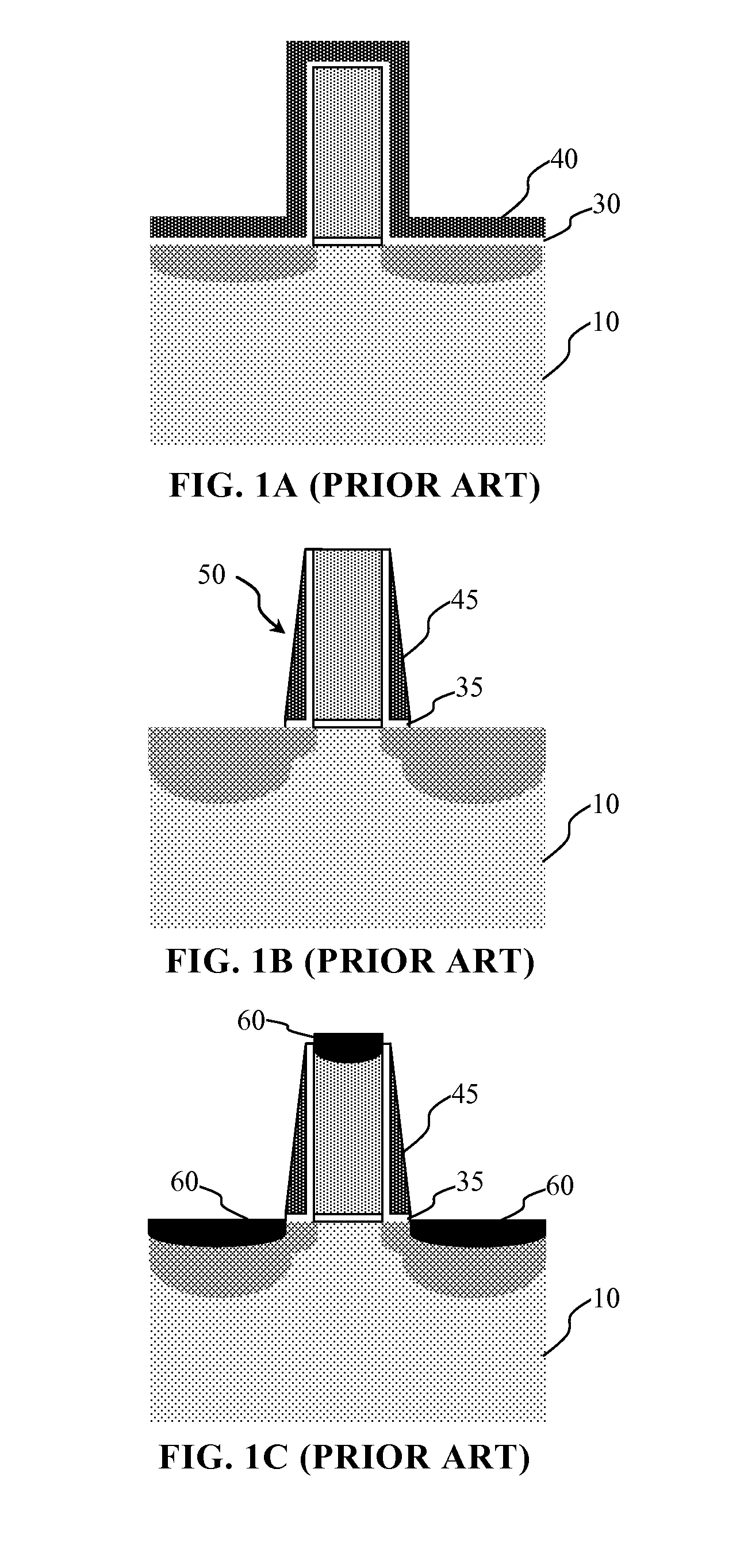
This application claims priority to Chinese Patent Application No. 201110131064.1, filed on May 20, 2011 and entitled “SEMICONDUCTOR DEVICE AND MANUFACTURING METHOD THEREOF”, which is incorporated herein by reference in its entirety. 1. Field of the Invention The present invention relates to semiconductor techniques, and more particularly to semiconductor devices and manufacture methods thereof. 2. Description of the Related Art With the increasing development of semiconductor techniques, MOSFET feature size is continually reduced, drawing tremendous attention in the field to the issue of carrier mobility reduction, and consequently leading to several schemes of carrier mobility enhancement. Some of such schemes realize carrier mobility enhancement through applying stress to MOSFET channel region. Through applying stress to the channel region of MOS device to induce strains in the channel region, it is possible to influence the carrier mobility in the channel region. Specifically, NMOS device is electron conductive, the larger the lattice spacing is, the smaller the effects of lattice scattering, and thus, a larger the electron mobility, as well as a driving current, can be achieved, therefore, it is desirable to apply a tensile stress to the channel to enlarge the crystal lattice; for PMOS device, on the contrary, the smaller the lattice spacing is, the larger the hole mobility is, so it is desirable to apply a compressive stress to the channel. A method of applying stress to channel region is the covering film stress technique. Depositing a stress film after forming silicide on source, drain and gate regions, a stress can be transmitted to the channel region, so that the device performance can be significantly affected. As an example of stress film, it is known that Si3N4film deposited by thermal chemical vapor deposition has tensile stress, while Si3N4film deposited by plasma chemical vapor deposition has compressive stress. In order to improve NMOS and PMOS device performance simultaneously, tensile and compressive stress films can be deposited on NMOS and PMOS devices respectively. For example, first, a tensile stress film can be deposited, and then it can be etched to remove the tensile stress film covering a PMOS device, and then a compressive stress film can be deposited, followed by removing the compressive stress film on a NMOS device. A stress proximity technique (SPT) is set forward to transmit stress into a channel region more successfully. That is, a sidewall spacer on opposite sides of the gate is reduced in thickness before stress film deposition to shorten the distance between the stress film and the channel region, so that the stress in the stress film can be transmitted into the channel region more effectively. Consequently, a better effect can be achieved. Next, a SPT implementation method will be described with reference of First, as shown in Next, as shown in Next, as shown in Next, as shown in Then, as shown in Since the thicker silicon nitride portion 45 is removed after defining the source and drain regions with the spacer 50, the stress film 70 is placed more proximately to the channel region, such that the stress in the stress film can be transmitted into the channel region more effectively. As shown in Hence, a new SPT implementation method capable of avoiding silicide loss is highly desired. An aspect of this invention is to provide a method of manufacturing semiconductor devices, which can avoid silicide loss while realizing the stress proximity technique. According to one aspect of this invention, a method of manufacturing a semiconductor device is provided, which may comprise the following steps: forming a gate on a substrate; forming a stack including a first material layer, a second material layer, and a third material layer from inner to outer in sequence, to cover the surface of the substrate, the top surface of the gate, and opposite sidewalls of the gate; etching the stack to form sidewall spacers on opposite sidewalls of the gate, including the remaining portions of the first material layer, the second material layer and the third material layer; performing ion implantation to form a source region and a drain region on opposite sides of the gate respectively; partially or completely removing the remaining portion of the third material layer; performing a pre-cleaning process, wherein all or a portion of the remaining portion of the second material layer is removed; forming silicide on top of the source region, the drain region and the gate; depositing a stress film to cover the silicide and the remaining portion of the first material layer. Preferably, the remaining portion of the second material layer serves as a block layer when partially or completely removing the remaining portion of the third material layer. Preferably, the step of partially or completely removing the remaining portion of the third material layer may be implemented through a wet or dry etching process with a high selectivity ratio to the second material layer. Preferably, each of the first material layer and the third material layer may be a silicon nitride layer or a silicon oxynitride layer, and the second material layer may be a silicon oxide layer. Preferably, the stack may further comprise an oxide layer under the first material layer; the sidewall spacers may further comprise a remaining portion of the oxide layer; when performing the pre-cleaning process, the remaining portion of the first material layer serves as a block layer to prevent the oxide layer from being removed. Preferably, the oxide layer may be a silicon oxide layer. Preferably, when the channel region is n-type channel region, the stress film may be a tensile stress film. Preferably, when the channel region is p-type channel region, the stress film may be a compressive stress film. According to another aspect of this invention, a semiconductor device is provided, which may comprise: a gate on a substrate; a source region and a drain region respectively on opposite sides of the gate; silicide on top of the source region, the drain region, and the gate; an “L”-shaped first material layer located between the gate and the silicide on top of the source region, between the gate and the silicide on top of the drain region, and on the sidewalls of the gate, the first material having a lower selectivity ratio than an oxide in a pre-cleaning operation prior to the silicide forming process; and a stress film covering the silicide and the “L”-shaped first material layer. Preferably, the first material may be silicon nitride or silicon oxynitride. Preferably, the semiconductor device may further comprise an “L”-shaped silicon oxide layer located between the “L”-shaped first material layer and the substrate, and between the “L”-shaped first material layer and the sidewalls of gate. Preferably, the gate is adjacent to a channel region, and when the channel region is an n-type channel region, the stress film is a tensile stress film. Preferably, the gate is adjacent to a channel region, and when the channel region is a p-type channel region, the stress film is a compressive stress film. With the method disclosed above, silicide loss can be avoided while improving device performance through SPT. The accompanying drawings illustrate embodiments of the invention and, together with the description, serve to explain the principles of the invention. It should be noted that in those drawings those parts are not illustrated in actual proportion for the convenience of description. Next, an implementation of the method of manufacturing a semiconductor device will be described with reference to First, as shown in The second nitride layer 140 may be relatively thicker, while the first oxide layer 110, the first nitride layer 120, and the second oxide layer 130 may be relatively thinner. The first oxide layer 110 and the second oxide layer 130 may be silicon oxide layers, while the first nitride layer 120 and the second nitride layer 140 may be silicon nitride layers. Either or both of the first nitride layer 120 and the second nitride layer 140 can also be substituted with an oxynitride layer, for example, a silicon oxynitride layer. Next, as shown in Next, as shown in Next, as shown in The remaining portion 125 of the first nitride layer 120 is not removed in the pre-cleaning process, which in turn can preserve the remaining portion 115 of the first oxide layer 110. Next, as shown in Next, as shown in For a NMOS device region with n-type channel, a tensile stress film is deposited, and for a PMOS device region with p-type channel, a compressive stress film is deposited. As an example of the stress film, a Si3N4film deposited through thermal chemical vapor deposition can be utilized as the tensile stress film, and a Si3N4film deposited through plasma chemical vapor deposition can be utilized as the compressive stress film. However, the present invention is not limited to that example. As shown in As mentioned above, the “L”-shaped oxide layer 115 can be a silicon oxide layer, and the “L”-shaped nitride layer 125 can be a silicon nitride layer. If the first nitride layer 120 is substituted with an oxynitride layer, the “L”-shaped nitride layer 125 can be replaced with an “L”-shaped oxynitride layer. For NMOS devices with n-type channel, the stress film 170 may be a tensile stress film. For PMOS devices with P-type channel, the stress film 170 may be a compressive stress film. During the formation of the device, the remaining portion 145 of the second nitride layer 140 serves as a block in source-drain implantation to define a heavily doped region. Since the remaining portion 145 of the second nitride layer 140 is removed before silicide formation, it is unnecessary to remove nitride after silicide formation, avoiding the loss of silicide accordingly. When etching to remove the remaining portion 145 of the second nitride layer 140, the remaining portion 135 of the second oxide layer 130 serves as an etch block layer to preserve the remaining portion 125 of the first nitride layer 120 (“L”-shaped nitride layer) and the remaining portion 115 of the first oxide layer 110 (“L”-shaped oxide layer). A certain distance between the silicide 160 formed on the source and drain regions and the channel is generated due to the presence of the “L”-shaped nitride layer 125 and the “L”-shaped oxide layer 115, avoiding shorting the silicide 160 to the channel. The preferable embodiment of this invention has been described in detail above, wherein, first, a stack 105 is formed including the first oxide layer 110, the first nitride layer 120, the second oxide layer 130 and second nitride layer 140. However, from the analysis of the functions of those layers, the effect of this invention can be achieved by merely forming three layers (which can be referred to as “the first material layer”, “the second material layer”, and “the third material layer” from inner to outer). Below, another implementation of manufacturing semiconductor device with a three-layer stack will be described with reference to First, as shown in The third material layer 240 can be relatively thicker, and the first material layer 220 and the second material layer 230 can be relatively thinner. The second material layer 230 can be a silicon oxide layer, and the first material layer 220 and the third material layer 240 can be silicon nitride layers. Either or both of the first material layer 220 and the third material layer 240 can also be substituted with an oxynitride layer, for example, silicon oxynitride layer. Next, as shown in Next, as shown in Next, as shown in The remaining portion 225 of the first material layer 220 is not removed in the pre-cleaning process. Next, as shown in Next, as shown in For a NMOS device region with n-type channel, a tensile stress film is deposited, and for a PMOS device region with p-type channel, a compressive stress film is deposited. As an example of the stress film, a Si3N4film deposited through thermal chemical vapor deposition can be utilized as the tensile stress film, and a Si3N4film deposited through plasma chemical vapor deposition can be utilized as the compressive stress film. As shown in As compared to the semiconductor device shown in In this embodiment, upon etching to form the sidewall spacers including the remaining portions of the first material layer, the second material layer, and the third material layer, the remaining portion of the third material layer is used to define the heavily doped region in source-drain ion implantation. When etching to remove the remaining portion of the third material layer, the remaining portion of the second material layer serves as a block layer, to preserve the remaining portion of the first material layer beneath. The first and second material layers have different properties, in the pre-cleaning performance and the like, the first and second material layers have different selectivity ratios, so that the remaining portion of the first material layer can be retained while partially or completely removing the remaining portion of the second material layer. The remaining portion of the first material layer defines the areas of forming silicide on source region and drain region, ensuring a certain distance between the channel region and the silicide on source region and drain region, accordingly, avoiding the risk of shorting the silicide to the channel region. It can be seen that forming the aforementioned stack including the first material layer, second material layer, and third material layer can achieve the effect of this invention. In addition, other material layers can be added as required. Also, the first material layer, second material layer, and third material layer are not limited to the specific embodiments exemplified above, so long as they can function as above described respectively. Further, the thickness of the third material layer can be determined by the thickness designation of the sidewall spacers. The second and first material layers can be thin to such an extent that it is sufficient to stop the etching process when an upper layer is removed. In this way, upon removing the third material layer finally, the distance between the deposited film and the channel region can be considerably reduced. Hence, the present invention provides a method of manufacturing semiconductor device, which comprises the following steps: forming a gate on a substrate; forming a stack including a first material layer, a second material layer, and a third material layer from inner to outer in sequence, to cover the surface of the substrate, the top surface of the gate, and opposite sidewalls of the gate; etching the stack to form sidewall spacers on opposite sides of the gate, including the remaining portions of the first material layer, the second material layer and the third material layer; performing ion implantation to form a source region and a drain region on opposite sides of the gate respectively; partially or completely removing the remaining portion of the third material layer; performing a pre-cleaning process, wherein all or a portion of the remaining portion of the second material layer is removed; forming silicide on top of the source region, the drain region and the gate; depositing a stress film to cover the silicide and the remaining portion of the first material layer. Thus, the method of manufacturing semiconductor device as well as the semiconductor device formed by such a method have been described in detail according to this invention. Some details that are well known in the art are not described for the purpose of not obscuring the concept of this invention. With the above description, those skilled in the art can thoroughly understand how to implement the technique solutions disclosed herein. The above statement is given merely for illustration and description, and is not exhaustive, or to limit the invention to the disclosed form. Many modifications and changes are obvious to those skilled in the art. Embodiments are selected and described for a better illustration of the principle and practical application of this invention, so that those skilled in the art can understand this invention and envisage various embodiments with various modifications suited to specific usages. A semiconductor device and manufacture method thereof is disclosed. The method includes: forming a gate on a substrate; forming a stack including a first material layer, a second material layer, and a third material layer from inner to outer in sequence; etching the stack to form sidewall spacers on opposite sidewalls of the gate; performing ion implantation to form a source region and a drain region; partially or completely removing the remaining portion of the third material layer; performing a pre-cleaning process, wherein all or a portion of the remaining portion of the second material layer is removed; forming silicide on top of the source region, the drain region, and the gate; depositing a stress film to cover the silicide and the remaining portion of the first material layer. According to the above method, the stress proximity technique (SPT) can be realized while avoiding silicide loss. 1. A method of manufacturing a semiconductor device, comprising:
forming a gate on a substrate; forming a stack including a first material layer, a second material layer, and a third material layer from inside to outside in sequence to cover the surface of the substrate, the top surface of the gate, and opposite sidewalls of the gate; etching the stack to form sidewall spacers on opposite sidewalls of the gate, said sidewall spacers including the remaining portions of the first material layer, the second material layer and the third material layer; performing ion implantation to form a source region and a drain region on opposite sides of the gate respectively; partially or completely removing the remaining portion of the third material layer; performing a pre-cleaning process, wherein all or a portion of the remaining portion of the second material layer is removed; forming silicide on top of the source region, the drain region, and the gate; depositing a stress film to cover the silicide and the remaining portion of the first material layer. 2. The method according to 3. The method according to 4. The method according to 5. The method according to the sidewall spacers further comprises a remaining portion of the oxide layer; and when performing the pre-cleaning process, the remaining portion of the first material layer serves as a block layer to prevent the oxide layer from being removed. 6. The method according to 7. The method according to 8. The method according to 9. A semiconductor device, comprising:
a gate on a substrate; a source region and a drain region respectively on opposite sides of the gate; silicide on top of the source region, the drain region, and gate; an “L”-shaped first material layer located between the gate and the silicide on top of the source region, between the gate and the silicide on top of the drain region, and on sidewalls of the gate, the first material having a lower selectivity ratio than an oxide in a pre-cleaning operation prior to the silicide forming process; and a stress film covering the silicide and the “L”-shaped first material layer. 10. The semiconductor device according to 11. The semiconductor device according to 12. The semiconductor device according to 13. The semiconductor device according to CROSS-REFERENCE TO RELATED APPLICATIONS
BACKGROUND OF THE INVENTION
BRIEF SUMMARY OF THE INVENTION
BRIEF DESCRIPTION OF THE DRAWINGS
DETAILED DESCRIPTION OF THE INVENTION