SEMICONDUCTOR MANUFACTURING APPARATUS
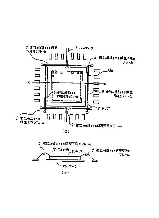
PURPOSE: To make a shape of a connected wire uniform, to simplify a process and to be used commonly for many kinds of packages by a method wherein, when a chip is connected to a package, a partition used to support the wire is provided. CONSTITUTION: A partition 13a which supports a wire 12 between a chip 2 and a package 1 is constituted by combining, e.g. six independent frames 3 to 8. Since these six frames 3 to 8 can be disassembled individually, a size of the partition 13a according to their combination can be changed to a large size or a small size by changing their combination size in order to comply with the package 1 and the chip 2 of different sizes. Accordingly, the partition 13a can be used commonly for the chip 2 of different sizes; the chip 2 and the package 1 can be connected while the wire 12 is supported by the partition 13a; even when a distance between the chip and the package is remote, the wire 12 to be connected does not sag and can be held in a definite shape. COPYRIGHT: (C)1990,JPO&Japio