소자 전사방법 및 소자 전사방법을 이용한 전자제품 제조방법
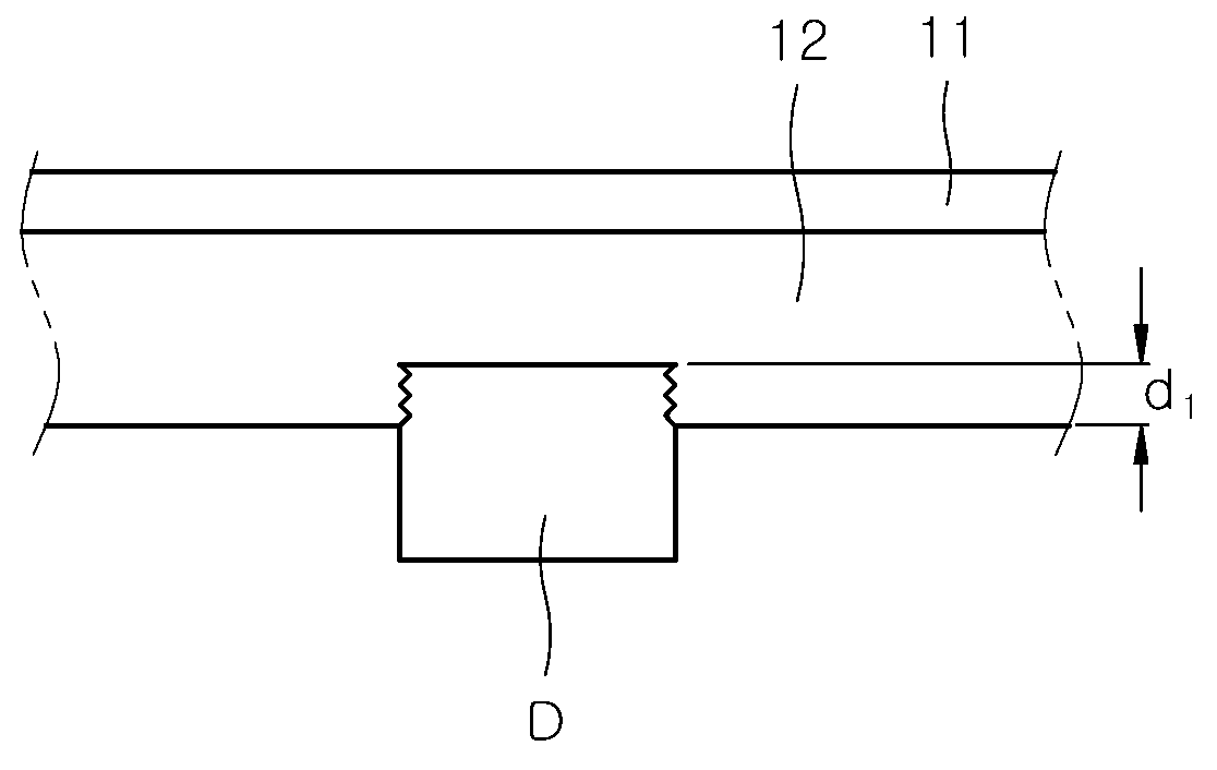
The present invention refers to carrier film, (device) transfer method and element transfer method using the same element number search using the same manufacturing method relates to article, more particularly element carrier film and substrate surface chemistry and transferred through removing blow-in depth fitted to a carrier film by adjusting number, (device) transfer method and element transfer method using the same element number using the same manufacturing method to article are disclosed. Generally, replace existing micro LED display using display of next generation tip display etc. to penetrate through. Such micro LED display module so as to obtain the highest each LED circuit board transferring core techniques is disclosed. Adhesive carrier film (adhesive carrier film) of the upper adhesive layer transfer process and a surface chemistry adjustment is possible only changes since the chemical components, such as the chemical components to be coated with adhesive having adhesive layer generally always in the same. The, adhesive carrier film existing between the substrate and the device using a carrier film when moving, relatively weak side of the wafer substrate carrier film during a relative movement only for stronger decreasing modulation signal, and vice versa id. is in principle. The, transfer unit of the device having a surface to which finding the proper adhesive layer is needed, basing the chemical components for the adhesive layer does not exist in a parallel pin is a deliquescing agent with respect to the direct number. In addition, constant when adhesive sheet having adhesive layer, the second transfer element is changed change number point cannot prevent adhesion along several kind of door to door which is transferring device of vertical handler number point pin is difficult. If the number of the present invention comprises a semiconductor substrate and a surface chemistry blow-in depth through the carrier film and press fitted by number, transferring the substrate to a desired carrier film or substrate to the gate number movement element carrier film, using the same method and element transfer method using the same element number (device) transfer a number article manufacturing method are disclosed. In order to solve the above-described and a number, the present invention refers to base film; and said formed on one surface of the base film, the adhesive layer number 1 transfer not element attached; wherein, said element and said number 1 pressure-sensitive adhesive layer is formed between the size of the adhesion between said number 1 characterized in that said element is a support film having an adhesive layer blow-in [kiph fitted to a proportional number substrate. Said base film on one surface of the base film and adhesive layer and a carrier film number 1, number 2 is the bottom face is formed on one adhesive layer including said base surface and urge the substrate, the second element said number 1 pressure-sensitive adhesive layer or said number 2 adhesive layer transfer are attached the pressing step; said first bar and said element and said element into said number 1 by the pressing step of the wafer adhesive layer formed between said number 1 number 1 number 1 adhesion adhesive layer forming step; said first bar and said element and said element into said number 2 by the pressing step of the wafer adhesive layer formed between said number 2 number 2 number 2 adhesion adhesive layer forming step; said carrier film from said release release step; wherein, the size of the element and said number 1 adhesive layer fitted to a proportional blow-in [kiph telephone number 1 for decreasing said number 1, the size of the element said number 2 blow-in [kiph telephone proportional number 2 fitted to a adhesive layer for decreasing said number 2, said number 1 blow-in [kiph telephone said number 2 by the difference between the element relative blow-in depth movement of the adhesive layer to the semiconductor layer between said number 1 to number said number 2 pressure-sensitive adhesive layer transfer method substrate. Said different said number 2 of the device to be formed said number 1 blow-in [kiph telephone blow-in depth, said number 1 adhesive layer adhesive layer can be adjusted in different viscoelasticity coefficient said number 2. Said different said number 2 of the device to be formed said number 1 blow-in [kiph telephone blow-in depth, said number 1 adhesive layer adhesive layer yield strength can be adjusted in a different yield strength and said number 2. Said number 1 said number 2 adhesive layer with a thickness that is different adhesive layer are formed to, said in the pressing step, said element said number 1 adhesive layer adhesive layer with a first thickness adhesive layer thickness said number 2 further pushed critical lower than the predetermined pressure applied to the substrate structure and said carrier film and said pressurizing force, said element said number 1 adhesive layer after forming the adhesive layer said element said number 2 adhesive layer adhesive layer adhesive layer with a first thickness said number 2 press fitted blow-in depth said number 1 corresponds to the deep blow-in [kiph fitted to a adhesive layer further can be disclosed. Said number 1 pressure-sensitive adhesive layer or said number 2 adhesive layer adhesive layer or adhesive by heat applied to said number 1 changes according to said number 2 hardness materials, said different said number 2 of the device to be formed said number 1 blow-in [kiph telephone blow-in depth, said number 1 heat due to the adhesive layer or adhesive layer can be adjusted in a different said number 2. Said number 1 adhesive applied to the adhesive layer and adhesive layer and said number 2 adhesive layer said number 1 wavelength of the light changes in accordance with said number 2 hardness materials, said different said number 2 of the device to be formed said number 1 blow-in [kiph telephone blow-in depth, said number 2 said number 1 adhesive layer can be adjusted in a different wavelength of the light irradiated adhesive layer. Said enclosed cylindrical roller carrier films are disposed, said uniform depth in the pressing step said number 1 is in contact adhesive layer is an entire flat projections projected from a surface of curved shape so that it can be formed into can be. Method of the present invention element transfer via the electronic number number of plate and by transfer on a number number article manufacturing method under the article on the chip tank substrate. The present invention according to carrier film, using the same manufacturing method using the same element transfer method and element transfer method number article the following effect flow tides. First, a ceramic micro device any desired substrate roller and plate combination continuous process may be performed in the memory disclosed. Second, existing chemically adjusted differently element about an apparently adhesion, carrier film, one of mechanical strain in a device using the substrate or carrier film occurs via a surface chemistry and transferring copyright 2001. According to one embodiment of the present invention indicating the example Figure 1 shows a carrier film also are disclosed. According to one embodiment of the present invention Figure 2 shows a sequence of method element transfer example also are disclosed. Figure 3 shows a method of indicating the status of the agent of of Figure 2 before the pressing step the element transfer are disclosed. Figure 4 shows a state after the pressing step of the method element transfer of Figure 2 also indicating are disclosed. Figure 5 shows a method element transfer in, for example the number 1 and number 2 adhesive layer adhesive layer indicating number 1 embodiment of Figure 2 also are disclosed. In Figure 6 shows a element transfer method, an adhesive layer and the adhesive layer of Figure 2 indicating the number 1 number 2 example number 1 embodiment variants also are disclosed. Figure 7 shows a element transfer method in, for example the number 1 and number 2 adhesive layer adhesive layer indicating number 2 embodiment of Figure 2 also are disclosed. Figure 8 shows a method element transfer in, number 1 and number 2 of Figure 2 indicating the adhesive layer adhesive layer example number 2 embodiment variants also are disclosed. Figure 9 shows a element transfer method in, to explain the urging force to the threshold of Figure 2 also are disclosed. Figure 10 shows a element transfer method in, for example the number 1 and number 2 adhesive layer adhesive layer indicating number 3 embodiment of Figure 2 also are disclosed. Figure 11 shows a method element transfer in, number 1 and number 2 of Figure 2 indicating the adhesive layer adhesive layer example number 3 embodiment variants also are disclosed. Figure 12 shows a element transfer method in, for example the number 1 and number 2 of Figure 2 indicating the number 4 embodiment adhesive layer adhesive layer also are disclosed. Figure 13 shows a method element transfer in, number 1 and number 2 of Figure 2 indicating the adhesive layer adhesive layer example number 4 embodiment variants also are disclosed. Figure 14 shows a element transfer method in, for example the number 1 and number 2 adhesive layer adhesive layer indicating number 5 embodiment of Figure 2 also are disclosed. In Figure 15 shows a element transfer method, number 1 and number 2 of Figure 2 indicating the adhesive layer adhesive layer example number 5 embodiment variants also are disclosed. Figure 16 shows a element transfer method in, for indicating the mobile carrier film using roller of Figure 2 also are disclosed. Figure 17 shows a carrier film carrier film from south to east blow-in [kiph this element of Figure 15 and also existing when attaching a region of carrier film pushed to account for the difference between surface and the device are disclosed. Hereinafter, the aforementioned constitution of the present invention in a preferred embodiment specifically number and can be realized with reference to the attached drawing examples described. The embodiment described in examples, the same name and the same code is employed and are identical in configuration, according to the additional description is omitted from to with each other. Specification in an entire layer, film, region, such as plate parts which are "on" when another area of said conduit when it "directly on" as well as to other parts of intermediate when comprises a unit. And "- on" means that the subject located above or below the multi-of which, which means that the gravity must be positioned on the upper side with reference to the direction does not. The entire specification of any component "comprising" a particularly when any portion that the opposite substrate can include other components without further means that the substrate. The size of the descriptions appearing in the drawing template for facilitating the arbitrarily revealing the thickness and the like, the present invention refers to just shown is not limited. With reference to fig. 1, the present invention according to a carrier film described as follows. As shown in fig. 1, the present invention according to a base film and a carrier (11) and, base film (11) formed on one surface of, the second transfer element (D) from adhering to the number 1 pressure-sensitive adhesive layer (12) comprises. Element (D) number 1 by the pressure is also an adhesive layer (12) is press-fitted into, element number 1 (D) on an adhesive layer (12) is formed between the size of the element number 1 (D) adhesion adhesive layer (12) is fitted to a blow-in depth (d1 ) Proportional to the other. Specifically, adhesive layer number 1 (12) (D) device and a method for of blow-in depth (d1 ) The greater the number 1 becomes large when the adhesive layer (12) and the device (D) is the contact between the edge portions are eliminated, the element number 1 (D) on an adhesive layer (12) the trust between 1,750,000. The, blow-in depth (d1 ) Diminishes the friction force becomes longer along thickness (D) number 1 is provided to the user on an adhesive layer (12) formed between increases as the magnitude of the wafer to be coated. Wherein, element number 1 (D) on an adhesive layer (12) of the wafer between undulated portion of Figure 1 indicated within a frequently occurring in order to substrate. Also with reference to 2 to 17 also, the present invention according to the method element transfer are described as follows. As shown in fig. 2, the present invention according to element transfer method is the pressing step (S10), the wafer forming step (S20) number 1, number 2 (S30) step (S40) of the wafer forming step heterocompounds without using a tool. First, as shown in (a) of Figure 3, element (D) with carrier film (10) and a bottom surface (21) on number 2 pressure-sensitive adhesive layer (22) is coated substrate (20) is provided and, carrier film (10) and the substrate (20) for aligning the parallels. In the pressing step (S10) said base film (11) base film (11) number 1 on one surface of the adhesive layer (12) formed a carrier film (10) and, the base plane (21) and the base plane (21) is formed on one surface of adhesive layer number 2 (22) including a substrate (20) against the other. Wherein the second element (D) is number 1 transfer adhesive layer (12) or number 2 pressure-sensitive adhesive layer (22) attached to the disclosed. I.e., number 1 of Figure 3 (a) as the element (D) is an adhesive layer (12) may be attached to the state the pressing step (S10) performed by, (b) of Figure 3 such as element number 2 (D) is an adhesive layer (22) of attaching a the pressing step (S10) is performed by disapproval. As shown in fig. 4, in the pressing step (S10) forming step (S20) for decreasing said number 1 received element number 1 is pressed by means of force (D) adhesive layer (12) press-fitted to the first bar element (D) number 1 on the adhesive layer (12) adhesion between number 1 (F1 ) Formed therein. In addition, in the pressing step (S10) forming step (S30) for decreasing said number 2 by heat received element (D) is number 2 (D) is urging force to the adhesive layer (22) press-fitted to the first bar element on number 2 (D) adhesive layer (22) between the wafer number 2 (F2 ) Formed therein. Number 1 adhesion (F1 ) Is the size of the element number 1 (D) adhesive layer (12) fitted to a number 1 to blow-in depth (d1 ) And proportional to, the wafer number 2 (F2 ) Is the size of the element number 2 (D) adhesive layer (22) is fitted to a number 2 blow-in depth (d2 ) On proportional to each other. Element (D) is number 1 pressure-sensitive adhesive layer (12) and number 2 pressure-sensitive adhesive layer (22) even when suspended from south to east, number 1 pressure-sensitive adhesive layer (12) and number 2 pressure-sensitive adhesive layer (22) or a property depending on the material number 1 blow-in depth (d1 ) Number 2 on blow-in depth (d2 ) And the difference is performed, the number 1 adhesion (F1 ) And number 2 adhesion (F2 ) Is equal to the difference occurs. In step (S40) release said carrier film (10) substrate (20) by element number 1 (D) release from the adhesive layer (12) or number 2 pressure-sensitive adhesive layer (22) separated from, element number 1 on which adhesive layer (D) release adhesive force (F1 ) And number 2 adhesion (F2 ) Determined by the relative difference. I.e., element number 1 for adhesion (D) (F1 ) For decreasing the number 2 (F2 ) Is greater than the element (D) is number 2 pressure-sensitive adhesive layer (22) mold release bar number 1 pressure-sensitive adhesive layer (12) and transferred, element number 1 for adhesion (D) (F1 ) For decreasing the number 2 (F2 ) Is smaller than element (D) is number 1 pressure-sensitive adhesive layer (12) mold release bar number 2 pressure-sensitive adhesive layer (22) are transferred. With reference to the adhesive layer 5 and 6 also different viscoelasticity coefficient also number 1 (12) and number 2 pressure-sensitive adhesive layer (22) of the number 1 in the embodiment is described as follows. As shown in of Figure 5 (a), element (D) is number 2 pressure-sensitive adhesive layer (22) attached to the, number 1 pressure-sensitive adhesive layer (12) viscoelasticity coefficient of number 1 (EA1 , ΗA1 ) Is number 2 pressure-sensitive adhesive layer (22) of viscoelasticity coefficient number 2 (EB1 , ΗB1 ) Than may have small value. The, number 1 pressure-sensitive adhesive layer (12) and number 2 pressure-sensitive adhesive layer (22) is the pressing step (S10) is pushed to a material can be composed by heat. As shown in (b) of Figure 5, the pressing step (S10) is passed through the element number 1 (D) adhesive layer (12) and number 2 pressure-sensitive adhesive layer (22) high strength corresponding, viscoelasticity coefficient number 1 (EA1 , ΗA1 ) On viscoelasticity coefficient number 2 (EA2 , ΗA2 ) Number 1 along the relative difference blow-in depth (dA1 ) Number 2 on blow-in depth (dA2 ) The size of the formed differently. Viscoelasticity coefficient number 1 (EA1 , ΗA1 ) Viscoelasticity coefficient is number 2 (EB1 , ΗB1 ) Than relatively small number 1 blow-in depth (dA1 ) The size of the number 2 blow-in depth (dA2 ) Formed to be larger than the size of, the, number 1 number 2 adhesion formed is relatively larger than chemistry, release step (S40) of Figure 5 (c) as shown in element (D) is number 1 through the adhesive layer (12) attached to the state number 2 pressure-sensitive adhesive layer (22) filled with a mold release. (D) such as element number 1 in the embodiment described above substrate (20) to release in carrier film (10) surface of the transferred, during semiconductor processing general component peaking process transferring the source substrate carrier film can be utilized. Also as shown in the present invention refers to not limited to 6, element number 1 (D) is an adhesive layer (12) and attached to the, number 1 pressure-sensitive adhesive layer (12) viscoelasticity coefficient of number 1 (EB1 , ΗB1 ) Is number 2 pressure-sensitive adhesive layer (22) of viscoelasticity coefficient number 2 (EB2 , ΗB2 ) May have a value greater than the. The, element (D) is number 1 blow-in depth (dB1 ) Number 2 on blow-in depth (dB2 ) According to the difference between the wafer adhesion than four relatively small number 1 number 2, release step (S40) through the element (D) is number 2 pressure-sensitive adhesive layer (22) of attaching a number 1 to adhesive layer (12) mold release encoded. The 3 (D) carrier film (10) release in to substrate (20) transferred step, an electrode is attached to the target substrate carrier film during semiconductor processing general beam pick-up phase process can be utilized. As a result, number 1 pressure-sensitive adhesive layer (12) and number 2 pressure-sensitive adhesive layer (22) of the band gap (D) transfer gate electrode (D) number exactness to determine the direction and is, a number 1 adhesive layer (12) and number 2 pressure-sensitive adhesive layer (22) can be according to the physical properties of reuse. With reference to different yield strength also 7 and 8 also number 1 pressure-sensitive adhesive layer (12) and number 2 pressure-sensitive adhesive layer (22) of the number 2 in the embodiment is described as follows. As shown in (a) of Figure 7, element (D) is number 2 pressure-sensitive adhesive layer (22) attached to the, number 1 pressure-sensitive adhesive layer (12) number 1 of yield strength (σA1 ) Is number 2 pressure-sensitive adhesive layer (22) number 2 of yield strength (σA2 ) Is smaller than the value. The, number 1 pressure-sensitive adhesive layer (12) and number 2 pressure-sensitive adhesive layer (22) is the pressing step (S10) is pushed to plastically deform by heat can be elastic material. As shown in (b) of Figure 7, the pressing step (S10) is passed through the element number 1 (D) adhesive layer (12) and number 2 pressure-sensitive adhesive layer (22) high strength corresponding, number 1 yield strength (σA1 ) Number 2 on yield strength (σA2 ) Number 1 along the relative difference blow-in depth (dC1 ) Number 2 on blow-in depth (dC2 ) The size of the formed differently. Number 1 yield strength (σA1 ) Is number 2 yield strength (σA2 ) Than relatively small number 1 blow-in depth (dC1 ) The size of the number 2 blow-in depth (dC2 ) Formed to be larger than the size of, the chemistry is relatively larger than number 1 number 2 adhesion formed, release step (S40) of Figure 7 (c) (D) as element number 1 is shown through the adhesive layer (12) attached to the state number 2 pressure-sensitive adhesive layer (22) filled with a mold release. The present invention refers to not limited to 8 as shown, element number 1 (D) is an adhesive layer (12) and attached to the, number 1 pressure-sensitive adhesive layer (12) number 1 of yield strength (σB1 ) Is number 2 pressure-sensitive adhesive layer (22) number 2 of yield strength (σB2 ) May have a value greater than the. The, element (D) is number 1 blow-in depth (dD1 ) Number 2 on blow-in depth (dD2 ) According to the difference between the wafer adhesion than four relatively small number 1 number 2, release step (S40) through the element (D) is number 2 pressure-sensitive adhesive layer (22) of attaching a number 1 to adhesive layer (12) mold release encoded. As a result, number 1 pressure-sensitive adhesive layer (12) and number 2 pressure-sensitive adhesive layer (22) (D) (D) the number of the target band gap exactness to determine transfer direction equal to or higher than the gate electrode. Reference number 1 of different thickness of 9 to 11 may also adhesive layer (12) and number 2 pressure-sensitive adhesive layer (22) of the number 3 in the embodiment is described as follows. First, using critical urging force to the broadcast receiver 9 also are described. The critical contact pressure acts specification number 1 pressure-sensitive adhesive layer (12) and number 2 pressure-sensitive adhesive layer (22) is formed such that the yield strength of the viscoelasticity coefficient and the conditions of e.g., number 1 pressure-sensitive adhesive layer (12) thickness of (t1 ) Number 2 on adhesive layer (22) thickness of (t2 ) When the X shaft, element number 1 (D) is an adhesive layer (12) and number 2 pressure-sensitive adhesive layer (22) with a first thickness of adhesive layer thickness further pushed sized big force. Number 1 pressure-sensitive adhesive layer (12) and number 2 pressure-sensitive adhesive layer (22) having a thickness the same, carrier film and the substrate when pressing a pressing force threshold, number 1 blow-in depth (dE1 ) Number 2 on blow-in depth (dE2 ) In the periphery of the element number 1 and number 2 can be compared with the adhesive layer is an adhesive layer which occur among different size of adhesion (Fc ) Is determined as resulting. As well as, carrier film (10) and the substrate (20) is less than the critical pressure even when apply pressure to number 1 blow-in depth (dE1 ) Number 2 on blow-in depth (dE2 ) Such as the size of the band and therefore, element number 1 (D) on an adhesive layer (12) and number 2 pressure-sensitive adhesive layer (22) which occur among different adhesion such as the size of the resulting. But, number 1 number 2 adhesive layer has a thickness of adhesive layer has a thickness relatively thinner than four, carrier film (10) and the substrate (20) when the first and pressing force (D) is lower than the predetermined pressure threshold to number 1 pressure-sensitive adhesive layer (12) fitted to a number 1 to blow-in depth (dE1 ) Component (D) is number 2 pressure-sensitive adhesive layer (22) is fitted to a number 2 blow-in depth (dE2 ) Smaller than that of the first silicon substrate. Number 1 pressure-sensitive adhesive layer (12) of the element (D) one surface of the base film (11) movement and flexibility number one, number 2 pressure-sensitive adhesive layer (22) is adapted to be press fit together with the element number (D) grudge without holes, number 1 blow-in depth (dE1 ) Number 2 than blow-in depth (dE2 ) Is equal to a large value. Blow-in depth according to the difference, for decreasing the size of the size of the number 2 number 1 adhesion (Fc ) Formed to be larger than. As shown in (a) of Figure 10, number 1 pressure-sensitive adhesive layer (12) thickness of (tA1 ) Is number 2 pressure-sensitive adhesive layer (22) thickness of (tA2 ) Is formed thinner than, carrier film (10) and the substrate (20) is a method of forming a number 1 (D) adhesive layer (12) thickness of (tA1 ) Subjected to a force that acts to the fitted to a threshold lower than the predetermined pressure. The, number 1 blow-in depth (dF1 ) The size of the number 2 blow-in depth (dF2 ) Formed thereof smaller than, the number 1 and number 2 relatively less adhesion than chemistry, release step (S40) of Figure 10 (b) as shown in element (D) is number 2 through the adhesive layer (22) of attaching a number 1 to adhesive layer (12) mold release encoded. Also as shown in the present invention refers to not limited to 11, number 1 pressure-sensitive adhesive layer (12) thickness of (tB1 ) Is number 2 pressure-sensitive adhesive layer (22) thickness of (tB2 ) Is formed thicker than the thickness, carrier film (10) and the substrate (20) is a method of forming a number 2 (D) adhesive layer (22) thickness of (tB2 ) Subjected to a force that acts to the fitted to a threshold lower than the predetermined pressure. The, element (D) is number 1 blow-in depth (dG1 ) Number 2 on blow-in depth (dG2 ) According to the difference between number 1 number 2 is relatively larger than the wafer adhesion formed, release step (S40) element (D) is number 1 through the adhesive layer (12) attached to the state number 2 pressure-sensitive adhesive layer (22) filled with a mold release. As a result, number 1 pressure-sensitive adhesive layer (12) and number 2 pressure-sensitive adhesive layer (22) of the thickness of, carrier film (10) and the substrate (20) is applied to the gate electrode (D) number of pressurized ununiform band gap (D) to determine the direction in which the transfer and releasing exactness is equal to or higher. Also with reference to other curable by heat 12 and 13 also number 1 pressure-sensitive adhesive layer (12) and number 2 pressure-sensitive adhesive layer (22) of the number 4 in the embodiment is described as follows. As shown in (a) of Figure 12, element (D) is number 2 pressure-sensitive adhesive layer (22) and attached to the, number 2 pressure-sensitive adhesive layer (22) is subjected to a constant temperature above the heat produced by the cured material, number 2 pressure-sensitive adhesive layer (22) heat evaporates the solvent and number 2 pressure-sensitive adhesive layer (22) and a bottom surface (21) may be disposed between, substrate (20) that is located outside the disapproval. As shown in (b) of Figure 12, adhesive layer number 2 and a heater (22) temperature (CA2 ) Is raised by number 2 pressure-sensitive adhesive layer (22) is cured and the, number 1 pressure-sensitive adhesive layer (12) to undergo a heat influenced by cured to substrate. The number 1 blow-in depth (dH1 ) The size of the number 2 blow-in depth (dH2 ) Formed to be larger than the size of the, number 1 number 2 adhesion formed is relatively larger than chemistry, release step (S40) of Figure 12 (c) subjected to surface as shown in, element number 1 (D) is an adhesive layer (12) attached to the state number 2 pressure-sensitive adhesive layer (22) filled with a mold release. The present invention refers to correspondingly limited as shown in (a) of Figure 13, element number 1 (D) is an adhesive layer (12) and attached to the, number 1 pressure-sensitive adhesive layer (12) is subjected to a constant temperature above the heat produced by the cured material, number 1 pressure-sensitive adhesive layer (12) evaporates the solvent and heat from the number 1 pressure-sensitive adhesive layer (12) and the base film (11) may be disposed between, carrier film (10) that is located outside the disapproval. As shown in (b) of Figure 13, and a heater number 1 pressure-sensitive adhesive layer (12) temperature (CB1 ) Is raised by number 1 pressure-sensitive adhesive layer (12) is cured and the, number 2 pressure-sensitive adhesive layer (22) to undergo a heat influenced by cured to substrate. The number 1 blow-in depth (dI1 ) The size of the number 2 blow-in depth (dI2 ) Smaller than that of nozzle holder to cover the, number 1 and number 2 relatively less adhesion than chemistry, release step (S40) of Figure 13 as shown in (c) while subjected to, element (D) is number 2 pressure-sensitive adhesive layer (22) of attaching a number 1 to adhesive layer (12) mold release encoded. As a result, number 1 pressure-sensitive adhesive layer (12) or number 2 pressure-sensitive adhesive layer (22) is cured by heat activation signal (D) consist of a material of the gate electrode (D) to determine the exactness of transfer and a releasing direction in which the number is equal to or higher. In addition, number 1 pressure-sensitive adhesive layer (12) hardenable by radiation of light may be disclosed. Also 14 and 15 also refers to the wavelength of the light curable by different number 1 pressure-sensitive adhesive layer (12) and number 2 pressure-sensitive adhesive layer (22) of the number 5 in the embodiment is described as follows. As shown in of Figure 14 (a), element (D) is number 2 pressure-sensitive adhesive layer (22) attached to the, number 1 pressure-sensitive adhesive layer (12) and number 2 pressure-sensitive adhesive layer (22) changes according to a wavelength of light emitting unit 70 is composed of a material. Number 1 pressure-sensitive adhesive layer (12) and number 2 pressure-sensitive adhesive layer (22) is relatively short light irradiation strongly resulting in the displayed level of curing. For example, the adhesive layer having relatively long wavelength visible light having a relatively short wavelength when irradiated than ultraviolet curing adhesive layer when irradiated adhesive layer relatively more processing advances. As shown in (b) of Figure 14, number 1 pressure-sensitive adhesive layer (12) wavelength of the light projected on the (WA1 ) Is number 2 pressure-sensitive adhesive layer (22) wavelength of the light projected on the (WA2 ) When longer than, number 2 pressure-sensitive adhesive layer (22) is number 1 pressure-sensitive adhesive layer (12) to prevent further advance compared to cure is number 1 blow-in depth (dJ1 ) The size of the number 2 blow-in depth (dJ2 ) Formed to be larger than the size of, the chemistry is relatively larger than the wafer number 1 number 2 formed. The release step (S40) of Figure 14 as shown in (c) is subjected to, element number 1 (D) is an adhesive layer (12) attached to the state number 2 pressure-sensitive adhesive layer (22) filled with a mold release. The present invention refers to correspondingly limited as shown in of Figure 15 (a), element (D) is number 1 pressure-sensitive adhesive layer (12) and attached to the, number 1 pressure-sensitive adhesive layer (12) and number 2 pressure-sensitive adhesive layer (22) changes according to a wavelength of light emitting unit 70 is composed of a material. As shown in (b) of Figure 15, number 1 pressure-sensitive adhesive layer (12) wavelength of the light projected on the (WB1 ) Is number 2 pressure-sensitive adhesive layer (22) wavelength of the light projected on the (WB2 ) When shorter than, number 1 pressure-sensitive adhesive layer (12) is number 2 pressure-sensitive adhesive layer (22) in the coin number 1 further advance compared to prevent blow-in depth (dK1 ) The size of the number 2 blow-in depth (dK2 ) Formed thereof smaller than, the number 1 number 2 formed at an outer portion of adhesion than the first chemistry. The release step (S40) of Figure 15 (c) subjected to surface as shown, element (D) is number 2 pressure-sensitive adhesive layer (22) of attaching a number 1 to adhesive layer (12) mold release encoded. As a result, number 1 pressure-sensitive adhesive layer (12) and number 2 pressure-sensitive adhesive layer (22) first and the degree to which a light signal which is cured to form a process (D) number (D) to determine the direction in which the exactness of transfer and releasing the gate electrode is equal to or higher. As shown in fig. 16, carrier film (10) can be moved by engagement with the roller (R). Specifically, carrier film (10) and is disposed along the cylindrical roller (R) enclosed, roller (R) about the rotating axis of rotational movement number 2 and adhesive layer (22) is attached to the element number 1 (D) adhesive layer (12) are transferred. The, element (D) is carrier film (10) and the substrate (20) depressurized the pressing step (S10) number 1 in adhesive layer (12) and they are in element (D) to a uniform depth of an entire pushed, number 1 pressure-sensitive adhesive layer (12) is projected from a surface of curved shape forming a flat projections (12a) having a predetermined wavelength. Number 1 of curve shape having adhesive layer (12) and, flat projections (12a) number 1 having an adhesive layer (12) is removed (D) inserted slot depth (d3 ) When the same, shown in (a) of Figure 17 in place of an adhesive layer having curvilinear number 1 (12) (D) shown in (b) of Figure 17 to press-element region of the flat projection (12a) formed smaller than the area of the press-fitted element (D). Specifically, of Figure 17 (a) of the roller (R) shown in element (D) conferred on the largest by blow-in depth (d3 ) Having a wafer from the center of the adhesive is formed from a relatively small number 1 due to non-uniform X2 blow-in depth, (b) of Figure 17 shown in element (D) has a planar projection (12a) uniform blow-in depth (d3 ) Strength corresponding to, number 1 in addition adhesion uniformly formed. The flat projections (12a) including number 1 a adhesive layer (12) is more stable than a number 2 elements (D) adhesive layer (22) release from to be employed therein. On the other hand, a device using a roller (R) generally (D) case, roller (R) load number through substrate (20) where a thin metal can. The roller (R) in that it provides additional flat projections (12a) without forming a, roller (R) substrate (20) number by using only the contact load acting between the substrate (20) number 1 in contact with the adhesive layer (12) to regulate the size of, substrate (20) number 1 in contact with the adhesive layer (12) can be thin metal area of, the number 1 is formed as a flat adhesive layer (12) in the area of uniform blow-in [kiph this element (D) is pushed is equal to or higher. The, substrate (20) is made of the butanes. The present invention refers to correspondingly limited, carrier film (10) can be formed flat, is made of a carrier film (10) number 1 (D) ion implantation is performed on the adhesive layer (12) is formed in the uniform layer is formed on the wafer blow-in depth between number 1 can be stably transferring element is equal to or higher. Hereinafter, a method of the present invention element transfer plate and by transfer on electronic number number bath together by use of electronic number article is described other article manufacturing method. Wherein, element is micro LED can be, electronic number article such as a flat display or digital (digital signage) specifically between electronic components such as a circuit board or article number be inter-perfect electronic number. Circuit board include printed circuit boards, liquid crystal circuit board, display panel circuit board, such as a publicly known signal in various corresponding to this substrate, printed circuit board include publicly known soft, including both the circuit board can be rigid or around year, the present invention according to element transfer method described above can be electronic by article number number high pressure liquid coolant. As the device, the present invention refers to the above-mentioned specific preferred embodiment example correspondingly defined, in the claims claim the subject matter of invention without deviating from the invention various modifications in person with skill in the art is provided to embodiment of the present invention is capable of this transformation by ranges. D: element 10: Carrier film 11: Base film 12: Number 1 pressure-sensitive adhesive layer 12A: flat projection 20: Substrate 21: The base plane 22: Number 2 pressure-sensitive adhesive layer R: roller A carrier film according to an embodiment of the present invention omprises: a base film; and a first adhesive layer formed on a surface of the base film such that an element to be transferred is attached to the first adhesive layer, wherein the magnitude of force of adhesion between the element and the first adhesive layer is in proportion to the depth of press-fitting at which the element is press-fitted into the first adhesive layer. Back number Number 1 on one surface of the base film and said base film carrier film and adhesive layer, said adhesive layer formed on one base surface and the bottom face having the adhesive layer including said number 1 number 2 urge the substrate in a different thickness, said number 1 element that is attached to the adhesive layer or adhesive layer transfer when said number 2 the pressing step; said first bar and said element into said element said number 1 by the pressing step said number 1 adhesive layer adhesive layer formed of the wafer number 1 number 1 voltage having a magnitude proportional blow-in [kiph telephone number 1 fitted to a adhesion forming step; said first bar and said element into said element said number 2 adhesive layer by the pressing step blow-in [kiph telephone number 2 voltage having a magnitude proportional to said number 2 number 2 fitted to a adhesive layer formed of the wafer number 2 adhesion forming step; said carrier film from said release release step; wherein, in the pressing step said, said element said number 1 adhesive layer adhesive layer with a first thickness adhesive layer thickness said number 2 further pushed critical lower than the predetermined pressure applied to the substrate structure and said pressurizing force said carrier film, said adhesive layer adhesive layer after forming the adhesive layer said number 2 said number 1 element said element said number 1 adhesive layer adhesive layer with a first thickness blow-in depth fitted to a further adhesive layer fitted to a deep blow-in [kiph which corresponds to the number 2, said number 1 blow-in [kiph telephone said number 2 by the difference between the element between said number 1 adhesive layer blow-in depth relative movement of the number 2 pressure-sensitive adhesive layer to the semiconductor layer transfer method. Back number Back number Back number Back number Back number According to Claim 2, said enclosed cylindrical roller carrier films are disposed, said said number 1 in the pressing step is in contact adhesive layer is formed to a uniform depth an entire flat projection projected from a surface of curvilinear pushed characterized in including the element transfer method. A element transfer method of number 2 or number 8 via the anti anti by transfer on electronic number plate and is formed on the article number bath electronic number article manufacturing method.