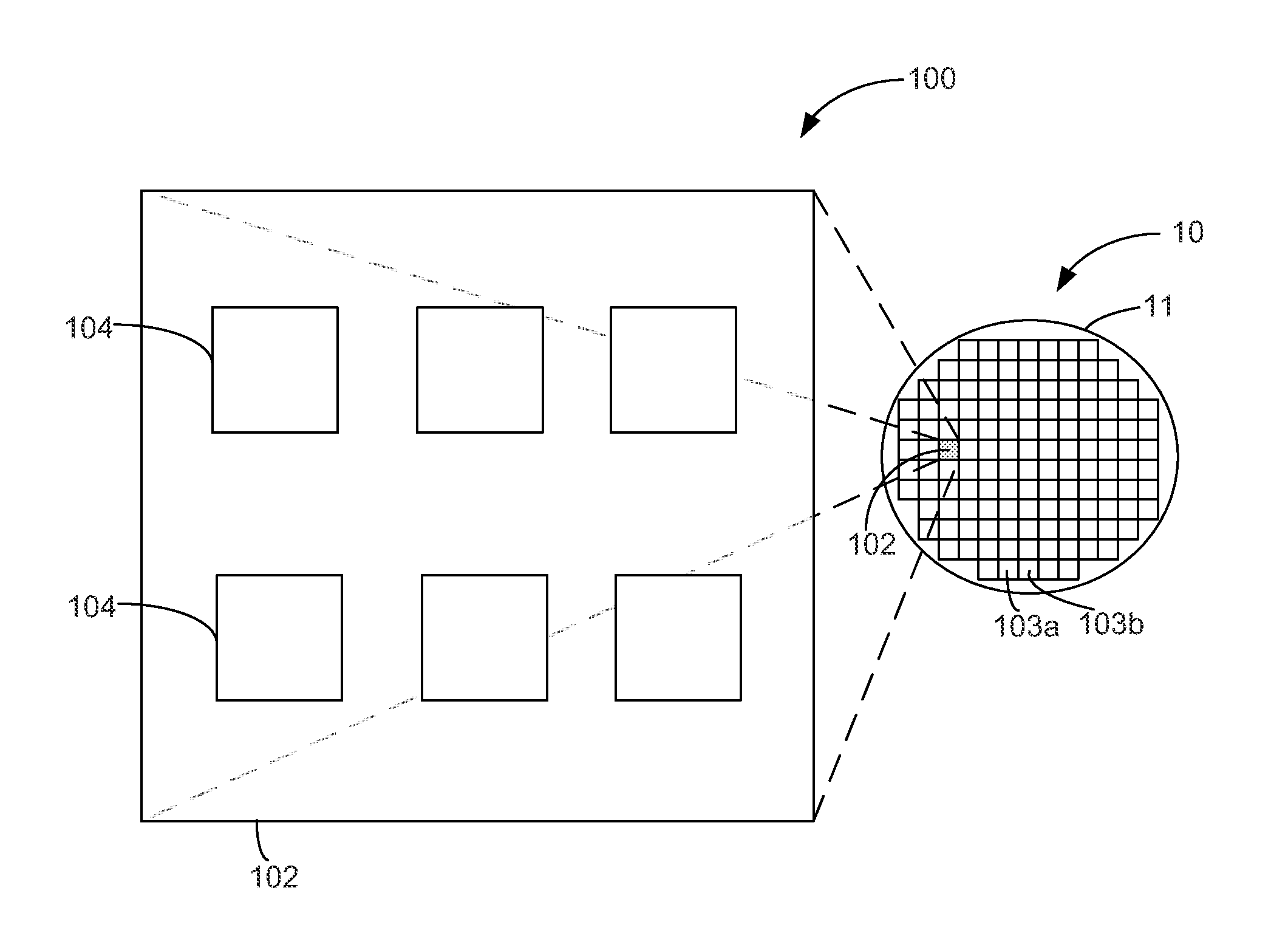
TSV들을 이용하는 통합된 마이크로폰 디바이스를 가진 다이
In the embodiment of the disclosure are generally integrated circuit field and, in particular, TSV (through a-silicon vias) are integrated using a die having a microphone device and associated configuration techniques and are disclosed. Microphone devices, e.g., communication devices, hearing aids are, polyurethane are used widely in various devices including the number [e[e] acoustic discriminating and noise. MEMS (micro electromechanical system) based microphone device miniaturization of electronic devices to direct the industrial tendency requires strong current integrating semiconductor chips etc.. However, such integration semiconductor chip semiconductor chip number it became grudge space brittle from congregating active circuit can be involved. Integration of MEMS based microphone peripheral environments where it is active circuit with key window, corrosive or other deleterious materials to the hereinafter for the introduction of the active circuit can be disclosed. In microphone device integration active side of the semiconductor chip are greater, more expensive chip can be requires. In the embodiment are associated with the attached drawing will next description will hereinafter for by. The order for description hereinafter, similar reference number in response specifying other structural elements. In the embodiment are for example defined in appended drawing glyphs of but shown as substrate. Also in the embodiment Figure 1 shows a plane view of the die in the form of an exemplary wafer form and method of singulating (singulated) some according to determine when etched. Figure 2 shows a also, some in the embodiment IC (Integrated Circuit) assembly according to determine under to do cross-sectional drawing the sides of the substrate. Figure 3 shows a capacitive transducer assembly also some in the embodiment according to determine under to do cross-sectional drawing the sides of the substrate. Figure 4 shows a cross-sectional drawing the sides of the microphone assembly according also some in the embodiment to determine the under to do substrate. Also some in the embodiment according to Figure 5 shows a side cross-sectional drawing in the other microphone assembly to determine under to do substrate. In the embodiment of Figure 6 shows a configuration of the microphone assembly according to the eyewear also some number 1 to determine under to do substrate. In the embodiment of Figure 7 shows a configuration of the microphone assembly according to the eyewear also some number 2 to determine under to do substrate. In the embodiment according to Figure 8 shows a configuration of the microphone assembly of the eyewear also some number 3 to determine under to do substrate. Figure 9 shows a microphone device according to an exemplary receiver circuit also some in the embodiment to determine the under to do substrate. Figure 10 shows a sum of the delayed signals including also some in the embodiment examples of an analog processing phased array output data to determine under to do substrate. Figure 11 shows a broadside configuration determine the phased array microphones also some in the embodiment according to exemplary under to do substrate. Figure 12 shows a phased array according to an exemplary beam steering using a microphone in the embodiment also some under to do determine the other. Figure 13 shows a layout of an exemplary membrane film plate and also some in the embodiment according to the eyewear microphone rear view to determine under to do substrate. In the embodiment according to various number bath is also 14a provided o cross-sectional drawing the sides of the microphone assembly during some aspect to determine the illustration as follows. Figure 15 shows a microphone assembly according to a method of flow determine the number bath also some in the embodiment under to do substrate. Figure 16 shows a specification also some in the embodiment according to the composition as described herein are an exemplary system determine the microphone assembly can be under to do substrate. The disclosure of TSV (through a-silicon vias) and related techniques and configuration in the embodiment are are integrated using a die having a microphone device is described as follows. In the following description, with reference to the appended drawing which form part of the specification, wherein the same portions throughout the specification and drawing the symbols indicating the same, in the disclosure content of the claimed subject matter is drawing in the embodiment are one [le[le] Tray [syen[syen] etc. can be shown by embodiment. The disclosure content of other wider in the embodiment may be utilized and structural or logical alterations are made in addition are may be accomplishing understanding. Therefore, detailed description is interpreted as meaning the adversary to hereinafter but number and, in the embodiment of range defined by appended claims and equivalent. The content for the purposes of disclosure, "A and/or B" known as phrase are (A), (B), or (A and B) big. The content for the purposes of disclosure, the phrase "A, B, and/or C" (A), (B), (C), (A and B), (A and C), (B and C), or (A, B and C) big. The present disclosure relates to upper/lower, side, such as described below can be using on/time based. This description are, and be used only for discussion hereinafter, the specification number only in one direction for any particular application of the subject matter described in the embodiment are intended to valve timing are not correct. The present disclosure relates to "in in the embodiment" or "in the embodiment in" can be provided using the phrase, each lapse of the same or different in the embodiment can be one or more. Furthermore, the disclosure such as used in the embodiment of association, "(comprising) including", "having (including)", "(having) having", and similar terms are the synonym are disclosed. "(Coupled with) comes into engagement with a" together with the specification can be used in terms of true derivative [e[e]. ". ". ". "". "Coupled" means the can be one or more. ". ". ". "". "Coupled" utilizes two or more element is direct physical or electrical contact with return electrode state can be. However, "coupled" in addition two or more elements of the fixing means which cooperate with the receptor to indirectly contact but still can be, and the one or more other elements is interconnected referred elements can be connected or coupled between components. ". ". ". "". The term "directly coupled" that the two or more elements of a return electrode can be direct contact state. In various in the embodiment, "number 2 characterized phase of the driving, or deposited, or otherwise arranged in feature number 1" that the representation can be characterized on number 1 or number 2 features formed over, or deposited, disposed, feature number 1 and number 2 direct contact with at least a portion of at least some of the features (e.g., direct physical and/or electrical contact) state or indirect contact (e.g., having one or more features between another aspect of feature number 1 number 2) switched can be at. The specification as used in bar, the term "module" ASIC (Application Specific Integrated Circuit), electronic circuit, one or more software or firmware program (shared, dedicated, or group) executing processor and/or memory (shared, dedicated, or group), combinatorial logic circuit, and/or other suitable components lapse of or functionality described under public affairs number, it has been shown that some or, it has been shown that can be comprising. Figure 1 shows a also, according to some in the embodiment, wafer form (10) and singulating form (100) exemplary die (102) to determine the plane view of under to do substrate. In some in the embodiment, die (102) is, e.g. silicon or other suitable material such as semiconductor material wafer configuration that its components (11) (e.g., dies (102, 103a, 103b)) a plurality of die can be one. A plurality of die wafer (11) can be formed on the surface of. Each of the described specification such as one or more microphones device (104) including a semiconductor number be a repeating units of a product. Die (102) includes, e.g. one or more transistor device at least one channel to channel path number under public affairs movement of charge carriers in the body (e.g., pin structures, nanowires, plane body etc.) or source/drain regions can be circuitry such as transistor structures. In some in the embodiment, the receiver circuit of a microphone device circuit, sensor circuit or other circuit can be. For example, contacts, the vias and/or trenches interconnect structures are transistor structure such as electrical energy from one or more of users or to establish a reserved path can be combined with or be formed on transistor structures. For example, interconnect structures for delivery of number and/or a transistor threshold voltage and a gate electrode under public affairsunder public affairs number of mobile charge carriers in the operation of the device can be electrically coupled to the channel body. One or more microphones device (104) to a straight line but also for the specific configuration and cost reduction 1, one or more microphones device (104) die other embodiment examples (102) with a variety of other suitable placement on any of the depicted can be composed in addition which is greater than or smaller than dimensions for understanding may have negative accomplishing. After completing the process for preparing the product embodied by a number number semiconductor dies, wafer (11) is, semiconductor number "chips" number to each of the separate article (e.g., die (102)) is a under public affairs separated from each other singulated process be experienced. Wafer (11) in different size can be any. In some in the embodiment, wafer (11) about 25. Range of 4 mm to about 450 mm diameter. Wafer (11) is in the embodiment that includes first features in other differing magnitudes and/or other can. In some in the embodiment, wafer (11) be a thin wafer is. In the embodiment according to various, microphone devices (104) the wafer form (10) or singulating form (100) can be disposed on the semiconductor substrate. The specification described in the microphone device (104) is logic or memory, or it has been shown that die combinations (102) can be received. In some in the embodiment, microphone devices (104) is SoC (system provided on-a chip) can be part of the assembly. Figure 2 shows a also, according to some in the embodiment, IC (Integrated Circuit) assembly (200) to determine the sides of the cross-sectional drawing under to do substrate. In some in the embodiment, IC assembly (200) includes a package substrate (121) electrically and/or physically binds (hereinafter, "die (102)") comprising one or more dies can be. In some in the embodiment, package substrate (121) is, as shown, circuit board (122) can be electrically coupled. In some in the embodiment, integrated circuit (IC) assembly (200) in different in the embodiment according, die (102) and package substrate (121) and/or circuit board (122) can be one or more. Die (102) includes forming a CMOS devices in relation to the thin film deposition, lithography, etching such as semiconductor material (e.g., silicon) semiconductor number bath techniques made from isolated number articles can exhibit. In some in the embodiment, one or more microphones device (e.g., one or more microphones device of Figure 1 (104)) comprises a die (102) can be formed on. In some in the embodiment, die (102) comprises a processor, memory, either SoC or ASIC, or be a proportion of them comprising them. In some in the embodiment, e.g. such as die molding compound or an underfill material (not shown by) electrically insulating material (102) and/or die level interconnect structures (106) can be encapsulating at least a portion of. Die (102) is, for example, package substrate as described flip chip configuration (121) coupled directly with the wide variety including sequence in accordance with the package substrate (121) can be attached. In flip chip configuration, including circuit, die (102) side of number 1 ("active side" sometimes called soak), the S1, bumps, pillars (pillars), or die (102) package substrate (121) can be coupled electrically in addition other suitable structure such as die level interconnect structures (106) and the package substrate (121) to the surface of a substrate. Die (102) of the number 1 side S1, e.g. can be active devices such as transistor devices. Number 2 side (sometimes referred to as the "non-active side"), as can be positioned opposite the side S1 S2 back is number 1. Die (102) a conventional semiconductor substrate (102a), one or more devices layer (hereinafter "the device layer (102b)") and at least one interconnect layer comprising (hereinafter "the neck which is it is big neck [thu[thu] layer (102c)") can be. Semiconductor substrate (102a) is, in some in the embodiment, such as for example can be substantially comprised of bulk semiconductor material. The device layer (102b) is active devices such as transistor devices formed on a semiconductor substrate area which can exhibit. The device layer (102b) is, and/or source/drain regions of transistor devices e.g. body comprising structures such as can be. Interconnect layer (102c) is the device layer (102b) in active devices configured to path of electrical signals to or from them can be interconnect structures including. For example, interconnect layer (102c) setting and/or contacts the electrical path for horizontal lines (e.g., trenches) number under public affairs and/or vertical plugs (e.g., vias), or other suitable features can be comprising. In some in the embodiment, the device layer are TSV (102b) or interconnect layer (102c) number 2 side S2 is electrically coupled with the circuit disposed on the semiconductor substrate for features (102a) can be formed through. ". ". ". "". Described "TSV" or "TSV are" being used throughout but, silicon based substrates described structures that define such terms must understand not only accomplishing. I.e., the "TSV" or "TSV are" other suitable substrate material to be electrically connected to a substrate through vias (through-a substrate vias) can be generally defines. The device layer (102b) and interconnect layer (102c) in each of the multiple layers can exhibit some in the embodiment. In some in the embodiment, die level interconnect structures (106) the interconnect layer (102c) and in addition is electrically coupled with the die (102) and the other path of electrical signals between the electrical devices can be arranged to set. Electrical signals, e.g. die (102) includes an input/output (I/O) used in connection with the operations of signals and/or power/ground signals can be. In some in the embodiment, package substrate (121) is, e.g. ABF (Ajinomoto Build provided up Film) such as, core and/or build-up layers epoxy based laminate substrate are disclosed. Package substrate (121) is, e.g., glass, ceramic, or semiconductor substrate including in the embodiment are formed into other types can be in other suitable thickness in axial direction. Package substrate (121) die (102) or path of electrical signals from the die can be arranged to set comprising electrical routing features. Electrical path setting features is, e.g. package substrate (121) disposed on at least one surface of the insulating layer or traces (not shown by) and/or e.g. package substrate (121) for establishing a path of electrical signals through trenches, vias or other interconnect structures such as comprising internal setting path of features (not shown by) can be. For example, in some in the embodiment, package substrate (121) die (102) number of each die level interconnect structures (106) configured to pads (not shown by) receiving such as electrical path comprising features can be set. Circuit board (122) epoxy laminate such as electrically insulating material is formed on the printed circuit board (PCB) implementation being. For example, circuit board (122) is, for example polytetrafluoroethylene (polytetrafluoroethylene), FR-a 4 (Flame Retardant 4), FR-a 1 (phenolic cotton paper) materials such as phenol nose [thun_ci[thun_ci], CEM-a 1 or CEM-a 3 nose [thun_ci[thun_ci] and epoxy materials such as, or epoxy resin prepreg material laminated together using materials such as woven glass material is that its components can be configured electrically insulating layers. Traces, such as interconnect structures (not shown by) trenches or via the circuit board (122) through a die (102) to establish a reserved path of electrical signals of electrical insulating layers can be formed through. Circuit board (122) is in other suitable materials other that its components can be configured in the embodiment. In some in the embodiment, circuit board (122) includes a mother board (e.g., motherboard of Figure 16 (1602)) are disclosed. For example, solder balls (112) such as the package level interconnects, package substrate (121) and circuit board (122) path of electrical signals between further arranged to set to form a corresponding solder joints (solder joints), package substrate (121) jacket and/or circuit board (122) on at least one pad (hereinafter, "pads (110)") can be coupled to. Pads (110) is, e.g. nickel (Ni), palladium (Pd), gold (Au), is (Ag), copper (Cu) and their combinations including electrically conductive material such as metal has any appropriate configuration that its components can be. Package substrate (121) on a circuit board (122) physical and/or electrical coupling for other suitable techniques can be use at the other in the embodiment. IC assembly (200) includes, e.g. flip chip and/or wire bonding configurations, interposers (interposers), SiP (system provided in a non-package) and/or PoP (package provided on a non-package) an appropriate combination of intermediate configurations including multi-chip package configurations, in a great variety of different in the embodiment other suitable configurations can be. Die (102) on the IC assembly (200) to establish a reserved path of electrical signals between other components of for other suitable techniques can be used in some in the embodiment. Also some in the embodiment according to Figure 3 shows a to reduce the capacitive transducer assembly (300) to determine the sides of the cross-sectional drawing under to do substrate. In the embodiment according to various, capacitive transducer assembly (300) is, as can recognize the, semiconductor substrate (102a) of a circuit (e.g., circuit (314)) formed on number 1 side S1, semiconductor substrate (102a) formed on rear view of number 2 S2 side plate (316), and semiconductor substrate (102a) are formed through the TSV (322a, 322b, 322c) with (e.g., die of Figure 1 (102) or wafer (11) of) semiconductor substrate (102a) can be comprising. In some in the embodiment, circuit (314) is e.g., microphone device receiver or sensor circuit such as can be active circuit. In some in the embodiment, circuit (314) of Figure 2 is the device layer (102b) can be comprising. Circuit (314) one or more of the interconnect layer of interconnect structures (e.g., trenches or vias) can be further comprises. In some in the embodiment, circuit (314) is of Figure 2 interconnect layer (102c) can be comprising. Circuit (314) such that only one material (318) can be disposed rear view plate (316) dielectric material (320) can be disposed. Dielectric material (318, 320) is further provided for example, silicon oxide (Si02 ) And similar can be any suitable material such as. In some in the embodiment, rear view plate (316) semiconductor substrate (102a) re-distribution layer (RDL: redistribution layer) S2 side of number 2 can be formed by patterning. In some in the embodiment, rear view plate (316) is rear view plate (316) formed through the at least one opening (316a) can be a. As can be ascertained, the TSV (322a, 322b, 322c) semiconductor substrate (102a) can be formed through. In some in the embodiment, one or more of the TSV S1 side circuit pattern on number 1 (314) on rear view plate (316) path of electrical signals between components such as number 2 side on microphone device arranged to set an S2 signal TSV (322a) implementation being. In some in the embodiment, when an operating state, rear view plate (316) is electrically active sensing electrode can be configured to act, TSV signal circuit (e.g., 322a) (314) (e.g., sensor circuit) electrical connection to under public affairs number can be configured. One or more of the TSV semiconductor substrate (102a) of number 1 and number 2 side S2 S1 side configured to path between ground signals are ground TSV (322b) implementation being. In some in the embodiment, are ground TSV (322b) of capacitive transducer assembly (300) external to the another electric device (e.g., another die, package substrate, interposer or circuit board) electrically coupled to interconnect structures on S1 side configured to number 1 (324) can be associated with (e.g., pads or contacts). One or more of the TSV rear view plate (316) such as microphone device components are structurally configured to support a support TSV (322c) implementation being. For example, the support TSV (322c) function as support pillar can be dummy TSV are. The support TSV (322c) circuit (314) on rear view plate (316) arranged to set an path of electrical signals between may not disclosed. In one in the embodiment, the support TSV (322c) can be at least partially filled with the electrically insulating material. In the embodiment according to various, semiconductor substrate (102a) is also 1 and as disclosed relating to die (102) portion of wafer form (10) or singulating form (100) can be represented. Capacitive transducer assembly (300) includes a single microphone or as part of some in the embodiment can be used as part of the microphone array. Figure 4 shows a also some in the embodiment according to the microphone assembly (400) to determine under to do cross-sectional drawing the sides of the substrate. In some in the embodiment, microphone assembly (400) of Figure 3 includes a capacitive transducer assembly (300) can be a. In the embodiment according to various, microphone assembly (400) includes, as can recognize the, semiconductor substrate (102a) of a circuit (e.g., circuit (314)) formed on number 1 side S1, S2 number 2 formed on a semiconductor substrate side rear view plate (316), and semiconductor substrate (102a) are formed through the TSV (322a, 322b, 322c) with (e.g., die of Figure 1 (102) or wafer (11) of) semiconductor substrate (102a) can be comprising. Microphone assembly (400) includes, as can recognize the, for rear view to form a capacitor plate (316) coupled to the membrane film (326) and membrane film (326) (e.g., lying below) adjacent semiconductor substrate (102a) to the chamber (303) can be further comprise. At least one opening (316a) is rear view plate (316) and/or dielectric material (320) may be formed through the one or more opening (326a) to the membrane film (326) can be formed through. Sacrificial material (325) to the membrane film (326) and rear view plate (316) can be disposed between. Sacrificial material (325) is sacrificial material (325) the region occupied by air gap under public affairs number to microphone assembly (400) number of number 1308. bath during the wetting ability. Chamber (303), openings (316a, 326a), and sacrificial material (325) region of the, various in the embodiment are removed in any suitable for e.g. air can be filled with a gas. Openings (316a, 326a) number can be under public affairs are gas outlet. In some in the embodiment, microphone assembly (400) includes a microphone device (e.g., microphone device of Figure 1 (104)) rear view plate (316), membrane film (326), chamber (303), the TSV (322a, 322b, 322c), openings (316a, 326a), sacrificial material (325) and the air gap region in which the occupied by/or circuit (314) can be one or more. Circuit (314) on opposite side rear view (e.g., number 2 side S2) components of a microphone device is coupled microphone devices on rear view side can be phased array that allows space under public affairs number. Such configuration, e.g., omni-directional or directional (hyper) such as heart-shaped (cardioid) desired acoustic pole pattern (directivity) digital delay - in order to increase the sensitivity and the sum beam-forming (digital delay-a and a-sum beam forming) can be corrected by microphone acoustic response allows. In some in the embodiment, semiconductor substrate (102a) and microphone device package substrate components (332) can be mounted on. For example, in the embodiment described in, number 1 S1 side solder bumps (330) and the package substrate (332) and coupled. An underfill material such as epoxy based undersell (328) or other suitable electrically insulative material, as can recognize the, semiconductor substrate (102a) confronts (332) can be disposed between. Solder bumps (330) the package substrate (332) and circuit (314) or e.g., power/ground and/or mouth/output (I/O) signals between the path of the microphone device can be arranged to set an electrical signals in other components. Semiconductor substrate (102a) in other suitable techniques and configurations other in the embodiment of the package substrate (332) can be combined with. In some in the embodiment, microphone assembly (400) includes a cover adapted to cover the microphone device components (334) can be a. Cover (334) is, for example, metal and semiconductor substrate can be configured that its components in addition (102a) mounted on a package board that its (332) can be combined with. Cover (334) comprises a die (e.g., semiconductor substrate (102a) and number 1 and number 2 formed on side S1 S2 side features) that forms a cavity surrounding the package for substrate (332) (e.g., flip chip substrate) can be combined with. In some in the embodiment, cover (334) is sound in particular for operation of the microphone device from entering the cavity to allow microphone assembly (400) under public affairs sound port number for at least one opening (334a) can be a. In some in the embodiment, upper port (e.g., one or more opening (334a)) includes a tablet devices can be suitable. Cover (334) cover (334) being covered by said microphone assembly (400) EMI (electromagnetic interference) for the components of the shielding can be under public affairs number. In the embodiment according to various, cover (334) is device number bath, wafer dicing (e.g., singulation) and/or can be configured to provide protection to a membrane film during packaging. Cover (334) and/or other in the embodiment may have other configurations that its components can be configured in other suitable materials. Also some in the embodiment according to Figure 5 shows a another microphone assembly (500) to determine under to do cross-sectional drawing the sides of the substrate. Microphone assembly (500) is of Figure 5 microphone assembly (500) is sound port under public affairs number for at least one opening (334a) under the outside number does not contain the microphone assembly (400) in the embodiment described in conjunction can be match to; rather package substrate (332) the microphone assembly (500) under public affairs sound port number for the package substrate (332) formed through the at least one opening (434a) without using a tool. In some in the embodiment, package substrate (332) semiconductor substrate is flip chip substrate (102a) is combined with a portion of the die flip chip substrate flip chip configuration are disclosed. As can be ascertained, at least one opening (434a) ambient gas (e.g., air) is cover (334) entry passageway for the number can be under public affairs surrounded by region. In some in the embodiment, at least one opening (434a) is be a duct for venting of the ultrasound imaging. In some in the embodiment, lower end (e.g., at least one opening (434a)) the mobile telephone device can be suitable. Figure 6 shows a according to some in the embodiment also, number 1 configuration according to microphone assembly (600) to determine the eyewear of under to do substrate. Number 1 configuration, single die in the embodiment which is described, wherein e.g., amplifier, bias circuit, phase shifter, delay - sum beamforming circuit, sigma delta modulator, phase shift delay (Td), and/or receiver circuit power generation and adjustment elements or other components such as active circuit (614) side of the device layer on die number 1 S1 (102b) disposed, e.g. one or more MEMS microphone transducer membrane film and/or rear view such as a slab microphone components (636) number 2 S2 is arranged on the side of the die. For example, microphone assembly single chip integrated into a MEMS microphone SoC implementation being. Microphone components (636) (e.g., broadside (broadside) configuration) acoustic wave of the air are useful for detection comprising membrane films can be exposed. In some in the embodiment, each microphone components described (636) the microphone and microphone device can exhibit discrete array of devices. Microphone assembly (600) of the configuration number 1 (e.g., interconnect layer (102c) - coupled to the die interconnect structures through) die number 1 another aspect of die or package such as package S1 side allows a flip chip assembly can be, number 2 side S2 on microphone components (636) can be directly exposed on the external sound. Membrane film disposed on the side of the die (e.g., number 2 side S2) rear view, another die or on the substrate flip chip mounting the membrane when exposed to incoming wavefront film die to allow positioning of the die (e.g., stacks of dies on) can be. Such a configuration allows the die is flip chip mounting, die die having an active side microphone components for wire bonding in contrast to acoustic wave to allow better membrane film exposing can be. Using the flip chip configuration, such as in example a mobile telephones or wearable devices, the smaller significantly reduced major implementations microphone assembly (600) for application of the hereinafter can be. Rear view side (e.g., number 2 side S2) on microphone components (636) positioning a, active circuit (614) (e.g., number 1 side S1) on a front side with a microphone components (636) placement of die size (e.g., about 50% size reduction) decreased can be allow. Die active circuit arrangement of said membrane film side rear view (614) more active devices such as front side of die (e.g., number 1 side S1) while further pair of, membrane film and active circuit (614) a short distance can be between under public affairs still number. In addition, active circuit (614) flip chip configuration can be shielded from the environment. In some in the embodiment, microphone components (636) active circuit (614) can be applied to bath followed by number, therefore, will not effect the active circuit process thereof can. According to various in the embodiment, as can be ascertained, microphone components (636) are corresponding to the one or more TSV (622) semiconductor substrate (102a) can be formed through. In some in the embodiment, the active circuit (614) includes a substrate (102a) through the path of electrical signals are arranged to set at least one TSV (622) using microphone components (636) can be combined with. Figure 7 shows a also, according to some in the embodiment, number 2 configuration according to microphone assembly (700) to determine the eyewear of under to do substrate. Number 2 configuration, multiple die in the embodiment which is described, wherein the active circuit (614) is, microphone components (636) is then formed on a die having a die electrically coupled (e.g., described in example die (702)) is arranged on the. E.g., microphone components (636) the active circuit die having (614) on microphone components (636) to establish a reserved path of electrical signals between a die level interconnect structures (106) using die (702) can be coupled to. One or more interconnect structures (e.g., the vias and/or trenches) (740) the die (702) of an active circuit (614) on microphone components (636) to establish a reserved path of electrical signals between the S2 side die having the number 2 of the interconnect layer (102c) can be formed. E.g., one or more interconnect structures (740) the microphone assembly (700) for inspecting (probing such as electronic inspection) parallel with the support and/or reference signals used for path setting under public affairs number to one or more of TSV (622) can be coupled to. In some in the embodiment, the configuration number 2 number 2 on transducer probing (e.g., probing reference plane) side S2 can be allow. In some in the embodiment, die (702) is another die (802) can be further attached to on. E.g., die (702) is microphone components (636) coupled directly to the S1 side die having an active side of number 1 (e.g., including active devices) and die level interconnect structures (106) using other dies (802) may have comes into engagement with a non-active side. Die (702) comprises a die (702) and the other die (802) arranged to set a path of electrical signals between at least one TSV can be. In one in the embodiment, die (702) is microphone components (636) for use connected to active circuit (614) may be a die including SoC (802) the memory or logic (e.g., processor) implementation being. In other in the embodiment, die (802) or die (e.g., die (702) and die (802)) combination of active circuit (614) can be a. In another in the embodiment, microphone components (636) is, for example, wire bonding, or other interposer configurations other suitable techniques such as another active circuit die (614) can be electrically coupled. Figure 8 shows a according to some in the embodiment also, number 3 configuration according to microphone assembly (800) to determine the eyewear of under to do substrate. Number 3 configuration, another multiple die in the embodiment which is described, wherein the active circuit (614) is microphone components (636) is then formed on a die having a die electrically coupled (e.g., in the embodiment depicted in die (702)) is arranged on the. Microphone assembly (800) is, of Figure 8 microphone assembly (800) is number 1 on transducer probing (e.g., probing reference plane) S1 side allow the second number under the outside microphone assembly (700) in the embodiment described by ALIGN with respect to the can. For example, in some in the embodiment, one or more signaling TSV (722), interconnect structures (740) and/or re-distribution layer (RDL) features (723) includes one or more signaling TSV (722) for feeding at least the risk of a membrane film from number 1 through S1 side can be formed to allow. Figure 9 shows a according also some in the embodiment, microphone device (e.g., microphone device of Figure 1 (104)) exemplary receiver circuit (900) to determine under to do substrate. Receiver circuit (900) includes a microphone output receiver can exhibit. In the embodiment according to various, as can recognize the, receiver circuit (900) calculates the (952) and phase shift delay (954) coupled to the TSV-a MEMS transducer (950) (e.g., capacitive transducer assembly of Figure 3 (300)) can be a. In some in the embodiment, individual microphone tone signal is phase shift delay (954) can be converted into a second stream to the first. Receiver circuit (900) is power generator block (956) can be further comprises, TSV-a MEMS transducer (950) for on - die high voltage bias generator (charge pump circuit) and pre amplifier (952) for silent power regulator comprising (silent power regulator) can be. In some in the embodiment, the specification described in the circuit (314) or active circuit (614) of Figure 9 includes a receiver circuit (900) can be a. Figure 10 shows a sum of phased array output data including also some in the embodiment according to delayed signals analog processing exemplary methodology (1000) to determine under to do substrate. Microphone array signal processing methodology (1000) in the embodiment can be executed by several delay sum beamforming. Phased array focus focused 'beam (beam-a like) similar' fax can be composed. For example, omni-directional, lobe direction parallel to beam pole pattern (directional) (hyper) such as heart-shaped directional microphone is, e.g. the electronically number can be disclosed. In some in the embodiment, the receiver circuit of each individual microphone (e.g., receiver circuit of Figure 9 (900)) is steering 220i block (1010) (e.g., filter) to output tone signals capable of feeding, the block can be introduced into a position delay tone signal. Example (1000) a common semiconductor substrate (102a) in addition microphone devices disposed on discrete output data adapted to process variable capacitors (e.g., capacitive transducer assembly of Figure 3 (300) or of Figure 9 TSV-a MEMS transducer (950)) and an array of amplifiers (e.g., of Figure 9 amplifier (952)) can be. Figure 11 shows a phased array microphones also some in the embodiment according to exemplary broadside configuration (1100) to determine under to do substrate. Broadside configuration (1100) in, as can be ascertained, microphone devices (e.g., microphone devices 1102, 1103, 1104) are incident acoustic wave (acoustic wave 1105, 1106) to isolate electric material devices can be integrated in broadside is orthogonal to the line. As can recognize the, respective output from microphone devices (e.g., microphone device 1102, 1103, 1104) can be are summed together. In Figure 10, programmable delay can be introduced into a tone signal. In some in the embodiment, subsequently in Figure 11, each individual microphone device (e.g., microphone device 1102, 1103, 1104) delayed tone signals can be added together by applying programmable weighting coefficients. Described microphone array signal processing can be executed by digital signal processing of die. In other in the embodiment, the form factor of their small size, multiple microphone array is end fired furnace (end-a fire) can be plural. Microphone devices in other suitable manners can be composed of other in the embodiment. Figure 12 shows a phased array according to an exemplary beam steering using a microphone in the embodiment also some under to do determine the other. Steering beam pattern (1202) non-steering beam pattern (1204) with described substrate. Steering non-pattern (1204) of the peak is centered in the 0 degree, steering beam pattern (1202) etched steering (1202) relatively shifted. Steering beam pattern (1202) DS noise cancellation noise source further toward steering 1308. In some in the embodiment, all phased array beamforming circuit in addition including phased array microphones can be disposed on a single die. Figure 13 shows a according also some in the embodiment, microphone rear view plate (316) and membrane film (326) exemplary layout (1300) to determine decomposition of the eyewear under to do substrate. In the embodiment according to various, membrane film (326) is rear view plate (316) on membrane film (326) die for lacing (102) side of rear view (e.g., number 2 side S2) comprising multiple storage apparatus ("legs") can be connected. For example, as described in the embodiment can be in a desired, membrane film (326) corresponding RDL pads (1333) 5 of legs including physical and electrical coupled to, one or more of the TSV pad (e.g., of Figure 4 are ground TSV (322b)) can be electrically and physically coupled in some in the embodiment. RDL pads (1333) and membrane film (326) of legs in aspects of the present invention physically and electrically coupling between a fridge to avoid causing a minimum vertical but represented by interrupted lines, vias or any other suitable interconnect structure can be achieved using. In some in the embodiment, each RDL pads (1333) (e.g., of Figure 4 are ground TSV (322b)) corresponding ground TSV can be electrically coupled. Rear view plate (316) air holes placed below the chamber (e.g., chamber of Figure 4 (303)) under public affairs number for at least one opening (316a) can be a. In some in the embodiment, RDL pad (1335) is rear view plate (316) and can be physically and electrically coupled. RDL pad (1335) signal (e.g., signal of Figure 4 TSV (322a)) TSV is such as its underlying TSV in some in the embodiment can be electrically and physically coupling. Membrane film (326) is described more or less than the legs and/or other in the embodiment can include other suitable configurations in rear view plate (316) can be configured in conjunction with. Cross-sectional area (1327) also is associated with a cross-sectional area to the upper portion of the description of 14a provided o can exhibit. In the embodiment according to various aspect is also 14a provided o some number bath during microphone assembly (1400) to determine the sides of the cross-sectional drawing illustration as follows. In the embodiment of Figure 13 in the sides of the cross-sectional areas is also 14a provided o cross-sectional drawing some (1327) can be comprising. The reference also 14a, die (102) S1 side of number 1 on circuit (e.g., the device layer (102b) and/or interconnect layer (102c) is formed, die (102) semiconductor substrate (102a) through the TSV (322) is formed, and die (102) of a microphone device S2 of number 2 on side rear view plate (316) formed of microphone assembly (1400) is described substrate. In some in the embodiment, the TSV (322) forming the circuit can be subsequently formed, rear view plate (316) is coupled to subsequently form a TSV can be executed. The TSV die number 2 side S2 before die with smaller thickness form (102) for under public affairs thinned by a number or to be elongated along the disclosed. In the embodiment acts in an appropriate order can be executed into other are other. Die (102) is, for example, carrier wafer (1444) and a die (102) configured to form a temporary bonding between adhesive number (1447) any suitable techniques including a carrier wafer (1444) can be combined with such as temporary carrier assembly. Carrier wafer (1444) comprises a die (102) side of number 2 number on die during tank S2 (102) can be used to for handling of hereinafter. Die (102) includes a interconnect layer (102c) coupled die in addition the circuitry (102) and a die (102) engage other components configured to path of electrical signals between the die level interconnect structures (106) can be comprising. Interconnect layer (102c) is the device layer (102b) and die level interconnect structures (106) configured to establish a reserved path of electrical signals between multiple layers of interconnect structures (e.g., trenches and/or vias) can be comprising. The device layer (102b) such as active device or microphone transistor circuit for use in connection with the operation of the device can be other components. The TSV (322) semiconductor substrate (102a) can be formed through the TSV are (322) at least some of the device layer (102b) and/or interconnect layer (102c) die (102) number 2 side of the device layer so as to set path of electrical signals between components on microphone device S2 (102b) and/or interconnect layer (102c) can be electrically coupled with the. In some in the embodiment, the TSV (322) TSV are individual, can recognize the bar and coupled together, barrier and/or seed layer (366), insulating layer (364) (e.g., oxide) and metal charging section (362) can be a. One or more passivation layer water, oxygen or other contaminants to protect from exposure to underlying components can be formed. In some in the embodiment, a passivation layer (320a) die (102) side of number 2 on semiconductor substrate S2 (102a) can be formed on. In some in the embodiment, a passivation layer (320a) die (102) through the TSV are S2 side of number 2 (322) can be deposited prior to forming. A passivation layer (320a) is, for example, silicon nitride (SiN) or silicon carbide (SiC) including a wide variety of suitable materials can be any one that its components configuration. Rear view plate (316) a passivation layer (320a) and TSV are (322) can be formed on. In some in the embodiment, rear view plate (316) the barrier and/or seed layer (1316) and barrier and/or seed layer (1316) disposed on e.g. a metal such as copper (1416) is that its components can be configured. Rear view plate (316) re-distribution layer (RDL) number for can be formed using a conventional high pressure liquid coolant. In some in the embodiment, a passivation layer (320b) is, as can be ascertained, rear view plate (316) and passivation layer (320a) can be formed on. A passivation layer (320b) a passivation layer (320a) similar to those described for that its components can be made out configuration. The reference also 14b, as can be ascertained, e.g. number 2 side S2 to coat a photosensitive material such as photoresist (1460) is deposited after the microphone assembly (1400) is described substrate. Photosensitive material (1460) is, for example, sensitive material (1460) to openings (e.g., openings 1460a, 1460b, 1460c) for forming lithography processes (e.g., exposure/developing) be patterned using be. For example, at least one opening (1460a) electrically connected and physically joined the barrier membrane of packets to be rear view plate (316) can be formed over the at least one of parts, at least one opening (1460b, 1460c) passivation layers (320a, 320b) in holes (e.g., with regard to the air hole) can be formed over on desired regions. The reference also 14c, as can recognize the, passivation layer (are) (320a, 320b) through openings (1460a, 1460b, 1460c) for extending the patterned photosensitive material (1460) etching of a microphone assembly (1400) is described substrate. The etching process is rear view plate (316) of underlying metal (1416) or the semiconductor substrate (102a) can be exposing a semiconductor material of one. In some in the embodiment, etching process is carried out, for example, dry etching such as plasma etching can include disclosed. In the embodiment comprising other etching process is carried out in other suitable techniques can be. The reference also 14d, photosensitive material (1460) stand-alone a number after the microphone assembly (1400) is described substrate. Photosensitive material (1460) is, for example, resist strip and/or cleaning any suitable number using the process of the wetting ability can be disclosed. The reference also 14e, die (102) of a sacrificial material on number 2 side S2 (325) depositing a mask of microphone assembly (1400) is described substrate. Sacrificial material (325) is in patterned sacrificial material (325) is sacrificial material (325) formation of membrane film onto a structural scaffold (structural scaffolding) and/or can be configured to mold the under public affairs number. For example, in some in the embodiment, sacrificial material (325) of the opening (1460a) is to expose while leaving openings (1460b and 1460c) can be configured to lower the charge. In some in the embodiment, sacrificial material (325) is adhesive number (1447) by bonding application process involves reacting a number can be formed at a temperature lower than the temperature, this temperature is about 200 °C may have a range of about 175 °C. Sacrificial material (325) is, for example, polypropylene carbonate-based material, photoresists, buffer coating materials including those and similar can be any suitable material. The reference also 14f, as can recognize the, membrane film (326) die (102) S2 is mounted on a lower side of number 2 of microphone assembly (1400) is described substrate. Membrane film (326) is, for example, PVD (physical vapor deposition), CVD (chemical vapor deposition), plasma - enhanced CVD, ALD (atomic layer deposition) and/or any suitable technique including a comprising at least one layer can be deposited. In some in the embodiment, membrane film (326) a passivation layer (320b) which is arranged on the adhesive layer, sacrificial material (325), and rear view plate (316) metal (1416), adhesive layer disposed on the metal layer disposed on the capping layer (capping layer) including a membrane and membrane metal layer comprising a stack of layers (not shown) can be. In one in the embodiment, adhesive layer is titanium nitride (TiN) and, membrane (Al) and aluminum metal layer, and a capping layer comprises TiN. The aluminum is a downstream etching processes can be used (e.g., XeF2 ) May have a selectivity for etching is compatible (compatible etch selectivity). Membrane film (326) can be other suitable materials in other in the embodiment. For example, copper or gold membrane that its components can be configured in other metal layer in the embodiment. The reference also 14g, membrane film (326) on sensitive material (1464) depositing a mask of microphone assembly (1400) is described substrate. For example, photosensitive material (1464) includes a membrane film (326) of desired number of special membrane film (326) over openings on the developing long fiber portion under public affairs number can be. The reference also 14h, membrane film by etching (326) number of stand-alone protection portion after the microphone assembly (1400) is described substrate. Etching process is carried out, for example, can be wet or dry etching techniques. Membrane film (326) is a TiN/Al/TiN including in one in the embodiment, chlorine based dry etch can be used. The reference also 14i, photosensitive material (1464) stand-alone a number after the microphone assembly (1400) is described substrate. Photosensitive material (1464) is, for example, resist strip and/or cleaning any suitable number using the process of the wetting ability can be disclosed. The reference also 14j, cavity layer (cavity layer) (1466) depositing a mask of microphone assembly (1400) is described substrate. In some in the embodiment, cavity layer (1466) polymer such as an epoxy-based material or other suitable material that its components can be configured. In the embodiment in several polymer thick, and optical definable (photodefinable) can be permanent. Cavity layer (1466) materials, e.g. spin (spin-a on) process and similar comprising die (102) number 2 side S2 of be any suitable techniques for coating can be deposited. As can recognize , the cavity has a rear view plate (316) and membrane film (326) over on hollow layers (1466) hollow layers so that it can be formed (1466) is rear view plate (316) and membrane film (326) for housing the outer peripheral surface partially to form the substrate. In some in the embodiment, the cavity is formed by patterning (e.g., exposure/development) can be. Several curing process in the embodiment of the cavity layer (1466) of deposited material can be executed. The reference also 14k, sacrificial material (325) stand-alone a number after the microphone assembly (1400) is described substrate. Sacrificial material (325) is, for example, thermal decomposition or wet/dry etching technique using any appropriate technique would number can be disclosed. Air sacrificial material (325) can be formed by a number of special fill the gap. The reference also 14l, semiconductor substrate (102a) chamber (303) formed of microphone assembly (1400) is described substrate. In the embodiment according to various, chamber (303) is a passivation layer (320a, 320b) can be formed by etching through openings in. For example, in one in the embodiment, a distillation xenon (XeF2 ) Plasma etch, silicon dioxide, silicon nitride, titanium nitride, aluminum, copper, gold, and the majority of numerous materials including polymers at room temperature vapor (gas phase) has approximately a selected ions into a semiconductor substrate (102a) isotropically etching silicon can be used. Chamber (303) for forming semiconductor substrate (102a) is formed on the resultant passivation layers (320a, 320b) formed through the air holes (e.g., openings of Figure 4 (316a)) can be run through. Other suitable etching processes and/state or the chamber (303) for use at the other in the embodiment form can be. In some in the embodiment, as can be ascertained, the TSV (322) at least one of the chamber (303) in the area of rear view plate (316) can be configured to support filler under public affairs number. The reference also 14m, cover (1434) to membrane film (326) and rear view plate (316) and/or surrounding or covering of microphone assembly (1400) is described substrate. In some in the embodiment, cover (1434) is, as can be ascertained, cover wafer and a cavity layer (1466) between bonding adhesive layer which is arranged on the surface to form a number (1436) can be wafer formed on a cover having, cover (1434) and cavity layer (1466) membrane film (326) and rear view plate (316) to form an enclosure around the substrate. Cover (1434) is, e.g. silicon, stainless steel, glass - reinforced epoxy or epoxy composite such as polymer based materials, including glass or any of a wide variety of suitable material is that its components can be configured. Adhesive number (1434) is, for example, wide variety of underfill and/or molding compound materials suitable materials including any one that its components can be configured. A bond, e.g., adhesive number (1434a) hardening, any suitable cover including a heat curing technique (1434) on the cavity layer (1466) can be formed between. Cover (1434) and cavity layer (1466) enclosure formed by, e.g. process such as during subsequent handling and/or mechanical damage during wafer bonding to number from microphone device protecting the components of the system can be. The 14n also reference, a temporary carrier (e.g., in the embodiment depicted carrier wafer (1444)) from a die having polished microphone device casing (102) of the separation of the microphone assembly (1400) is described substrate. In the embodiment according to various, carrier wafer (1444) is adhesive number (1447) weakly or an instrument for the die using heat process (102) from bonding to number with each other. In some in the embodiment, bonding the number of microphone assembly process is also 14m (1400) are on opposite sides of the concerned thermal contact with an a robot blade and processing for a (chuck) can be. In such in the embodiment, enlarging the microphone device casing cover (1434) can be protected by such damage during handling. Cover (1434) comprises a die (102) and method of forming components of a device in addition during microphone can be protecting. For example, die (102) is attached to the dicing frame on opposite sides of the adhesive wafer singulation microphone number while the dicing frame (mylar dicing frame) can be mounted onto the FEP with a circuit. Cover (1434) is, singulating die dicing frame number to tape reel (tape-a and a-reel) as it is disposed on anvil - - special devices and methods for protecting microphone can be. The reference also 14o, microphone assembly (1400) number for a sound port hole cover under public affairs (1434) through opening (1434a) formed of microphone assembly (1400) is shown substrate. Opening (1434a) is, e.g., including mechanical and/or laser apertures can be formed using any appropriate technique. In some in the embodiment, opening (1434a) is, during such membrane film (326) to reduce the risk of damage to the microphone assembly (1400) and method of forming and/or end packaging can be subsequently formed. Figure 15 shows a also some in the embodiment according to the microphone assembly (e.g., each number also 4, also 5 or 14o of microphone assembly (400, 500 or 1400)) a method 1500 for a number tank flow determine under to do substrate. The method 1500 also 1 to 4 described in the embodiment can be also the conformity with the reference, and vice versa are disclosed. 1502 in, the method 1500 number 1 side (e.g., S1 side 14a also of number 1), number 1 number 2 side and the second side (e.g., S2 also 14a side of number 2) and manufacturing method of number 1 side interconnect layer (e.g., also 14a of interconnect layer (102c)) a semiconductor substrate having a (e.g., semiconductor substrate also 14a (102a) the number can be a under public affairs. In some in the embodiment, a semiconductor substrate includes a semiconductor substrate interconnect layer number 1 disposed side of the device layer (e.g., the device layer of also 14a (102b)) can be further comprises. 1504 in, method 1500 through TSV semiconductor substrate (e.g., 14a are also of TSV (322) or are of Figure 4 TSV (322a, 322b, 322c)) comprising the steps of forming can be. In some in the embodiment, the device layer formed on the TSV is interconnect layer and/or following number 2 can be formed through the side of the semiconductor substrate. TSV is a circuit and/or interconnects active devices formed of the semiconductor substrate side of the semiconductor substrate is formed rotatably number 2 number 1 microphone device components can be arranged to set an path of electrical signals. For example, in one in the embodiment, the TSV device layer of active device and microphone device can be arranged to set between path of electrical signals. 1506 in, method 1500 semiconductor substrate number 2 side microphone device (e.g., microphone device of Figure 1 (104)) comprising the steps of forming can, microphone device electrically coupled to TSV. In some in the embodiment, microphone forming a device semiconductor substrate number 2 side rear view plate (e.g., plate or rear view of also 14o also 4 (316)) can be forming step. Rear view plate is electrically and/or physically TSV can be coupled. In some in the embodiment, the step of forming the magnetic layer rear view plate including patterning a metal can. In some in the embodiment, the step of forming the rear view on the microphone device to form a capacitor plate over membrane film (e.g., 4 or also 14o also membrane film (326)) further comprises the steps of forming can be. In some in the embodiment, the step of forming the membrane on the touch plate rear view a sacrificial material (e.g., also 14e of sacrificial material (325)) deposition step, the material of the membrane film on depositing sacrificial material, the sacrificial material and number can be a stand-alone. In some in the embodiment, the step of forming the membrane film adjacent to the microphone device or semiconductor substrate underlying the chamber (e.g., chamber or also 14l also 4 (303)) further comprises the steps of forming can be. Chamber is also described in connection with 14l techniques can be formed along. In some in the embodiment, the step of forming the microphone device cover (e.g., cover of Figure 4 (334) or also 14m cover (1434)) by cover can be a microphone device components. A semiconductor substrate includes a process of forming a microphone (also described by actions associated with 14a provided m) during at least part of a temporary carrier (e.g., also 14m carrier wafer (1444)) can be coupled to, following a temporary carrier from a microphone device semiconductor substrate covered with the cover combination can be number. The claimed invention in most help understand various operation object with a plurality of separate manner as an operation described in turn. However, the order of the parsing, such operations are necessarily order dependent means interprets back like that. The disclosure content required in the embodiment are as for configuring the hardware and/or software implemented in any suitable connected in response to can be. In the embodiment described in the specification as according to the some also Figure 16 shows a microphone assembly (e.g., each number also 4, 5 also 14o and also of microphone assembly (400, 500 or 1400)) can include a an exemplary system (e.g., computing device (1600)) to determine the under to do substrate. Computing device (1600) transfers the data between the enclosure (for example, housing (1608)) within a 1308. Motherboard (1602) comprises a processor (1604) and at least one communication chip (1606) but not limited only but it can be a plurality of components. Processor (1604) is a mother board (1602) can be physically and electrically coupled. In some embodiments, at least one communication chip (1606) also motherboard (1602) can be physically and electrically coupled. Additional implementations, communication chip (1606) comprises a processor (1604) can be part of. According to its application, computing device (1600) is a mother board (1602) or may be physically and electrically coupled to the other components may not can be coupled. These other components are, microphone device, volatile memory (e.g., DRAM (dynamic random access memory), non-volatile memory (e.g., ROM (read only memory)), flash memory, graphics processor, digital signal processor, password processor, chipset, antenna, display, touch screen display, touch screen number violations, battery, audio CODEC, video CODEC, power amplifier, GPS (global positioning system) device, compass, preamplifiers counter (Geiger counter), accelerometer, gyroscope, speaker, camera, and (hard disk drive, CD, DVD, etc. and such as) a mass storage device but, it in only field and not limited. Communication chip (1606) computing device (1600) to and from wireless communication transceiver can be histories. ". ". ". "". The terms "wireless" and derivative [e[e] true, non-modulated electromagnetic radiation over a medium through the use of data communications circuits, devices, systems, are method, techniques, communication channels, can be used to support other are described. The term, or may be otherwise in some in the embodiment, which are not related devices do not the summer solstice implies. Communication chip (1606) is Wi-a Fi (IEEE 802. 11 series), IEEE 802. 16 standards (for example, IEEE 802. 16 - 2005 correction), any correction are, update are, and/or updates are (e.g., advanced LTE project, UMB (Ultra Mobile Broadband) project (also referred to as "3GPP 2") or the like) including IEEE (Institute for Electrical and Electronic Engineers) involving LTE (Long Term Evolution) utilizes a standard but this number is one in only field but not exclusively, can be any of a number of wireless standards or protocols for implementing. IEEE 802. 16 compatible BWA (broadband wireless access) network are generally, IEEE 802. 16 standards evaluations for fit and interoperability through objects for a number authentication mark, representing a Worldwide Interoperability for Microwave Access abbreviation WiMAX network called substrate. Communication chip (1606) is GSM (Global System for Mobile Communication), GPRS (General Packet Radio Service), UMTS (Universal Mobile Telecommunications System), HSPA (High Speed Packet Access), E-a HSPA (Evolved HSPA), or can be LTE network operating in accordance with a. Communication chip (1606) is EDGE (Enhanced Data for GSM Evolution), GERAN (GSM EDGE Radio Access Network), operating in accordance with a UTRAN (Universal Terrestrial Radio Access Network) or E-a UTRAN (Evolved UTRAN) can be. Communication chip (1606) is CDMA (Code Division Multiple Access), TDMA (Time Division Multiple Access), DECT (Digital Enhanced Cordless Telecommunications), EV-a DO (Evolution-a Data Optimized), it has been shown that as well as them more, 3G, 4G, 5G, and those beyond any other wireless protocols can be designated as operating in accordance with a. Communication chip (1606) in other wireless protocols can be operating in accordance with other in the embodiment. Computing device (1600) comprises a plurality of communication chip (1606) can be comprising. For example, number 1 communication chip (1606) can be dedicated short-range wireless communications such as Bluetooth and the Wi-a Fi, number 2 communication chip (1606) is GPS, EDGE, GPRS, CDMA, WiMAX, LTE, such as EV-a DO can be dedicated long range wireless communication. Computing device (1600) processor (1604) is described in the specification as the microphone assembly (e.g., each number also 4, 5 also 14o and also of microphone assembly (400, 500 or 1400)) can be a. For example, die of Figure 2 and also 1 (102) includes a mother board (1602) mounted on a circuit board such as a package board that can be mounted on (e.g., package substrate (121)). ". ". ". "". The term "processor", registers and/or memory registers and/or memory embodiment of the electronic data from electronic data can be stored into other electronic data can lapse of portion of any device or device. Communication chip (1606) in addition the microphone assembly such as described in the specification (e.g., each number also 4, 5 also 14o and also of microphone assembly (400, 500 or 1400)) can be a. Additional implementations, computing device (1600) is within another component (e.g., SoC, ASIC, memory device or other integrated circuit device) is described in the specification such as microphone assembly (e.g., each number also 4, 5 also 14o and also of microphone assembly (400, 500 or 1400)) can be a. In various embodiments, computing device (1600) the mobile computing device, a laptop, net book, notebook, ultra book, smart phone, tablet, PDA (personal digital assistant), ultra mobile PC, mobile phone, desktop computer, server, printer, scanner, monitor, set-top box, the unit entertainment number, digital camera, portable music player, or be a digital video recorder. Additional implementations, computing device (1600) is processing data can be any other electronic device. Examples According to various in the embodiment, the disclosure is a device is described therein. Examples of the number 1 and number 2 side and the second side 1 side device semiconductor substrate having number 1, number 1 side of the semiconductor substrate formed interconnect layer, in addition number 1 and number 2 of the semiconductor substrate side of the semiconductor substrate formed through the semiconductor substrate side configured to path of electrical signals between TSV (through a-silicon via), and manufacturing method of number 2 side formed in addition TSV can be electrically coupled to a microphone device. Example 2 of device 1 is further provided and include, number 1 further includes a device layer formed side of the semiconductor substrate, wherein the device layer of active device and microphone device between the TSV is set consists of path of electrical signals. 2 example 3 of a device can be for example, the TSV has a plurality of TSV number 1 TSV and number 2 TSV microphone device during a plurality of TSV is structurally configured to support the device layer and in addition during and path of electrical signals between the microphone device not arranged to set. Device 1 is further provided comprising of 4 can be for example, the microphone device includes a semiconductor substrate to form a capacitor plate and disposed in addition TSV number 2 side comes into engagement with a rear view for rear view comprises a membrane film coupled to the plate. 4 example 5 of a device can be further provided, the microphone device further comprises a membrane film adjacent to the semiconductor substrate within the chamber. Example 6 of example 4 can be a device, adapted to cover the microphone device further comprises a cover. 6 example 7 of a device can be for example, a passivation layer of the semiconductor substrate wherein at least a portion of the passivation layer disposed side rear view plate number 2 - - arranged between the semiconductor substrate, and a passivation layer disposed on the cavity layer in addition having a cavity with a cavity that is associated with a layer of - - the membrane film layer further comprises a cavity and the cavity cover. Example 8 example 6 can be of a device, wherein the cover comprises a sound port holes. 6 example 9 is further provided of a device can be, including sound port hole further includes a flip chip substrate, wherein the semiconductor substrate may be combined with flip chip substrate which covers at least a flip chip configuration of the die, that forms a cavity to cover for combined with flip chip substrate, disposed in the cavity die, and sound sound to a porthole is a cavity passage number under public affairs substrate. The device can be of any of the examples 1 to 5 example 10 a, which covers at least a semiconductor substrate includes the die number 1, number 2 die is coupled die number 1, number 2 die receiver or sensor circuit comprises a microphone device. The device can be of any of the examples 1 to 5 example 11 a, the microphone device includes a semiconductor substrate formed side number 2 is one of the plurality of microphones. According to various in the embodiment, the disclosure is a method are described as follows. Examples of method number 1 number 1 and number 2 side and the second side includes a side 12, the semiconductor substrate having a semiconductor substrate and number 1 side interconnect layer number under public affairs, semiconductor substrate through the semiconductor substrate of the semiconductor substrate forming a TSV - TSV is number 1 side are configured to establish a reserved path of electrical signals - rotatably number 2, and manufacturing method of number 2 side microphone device comprising forming a TSV - microphone device can be electrically coupled. Method of example 12 and 13 include for example, the semiconductor substrate of the semiconductor substrate formed side number under public affairsunder public affairs number the number 1 further includes a semiconductor substrate having a device layer, the device layer of active device and microphone device between the TSV is set consists of path of electrical signals. 14 is further provided a method of 12 can be for example, the microphone forming a device semiconductor substrate forming step number 2 - TSV - rear view plate comes into engagement with a rear view side by, and a capacitor plate to form a film thereon to form a membrane over the rear view can be. Example 15 is further provided comprising method can be of 14, wherein the step of forming the membrane film depositing a sacrificial material on the touch plate rear view, on membrane film material depositing sacrificial material, the sacrificial material and industry number comprising the following steps. Example 14 method of comprising 16 can be for example, membrane defining a chamber further comprises semiconductor substrate adjacent membrane. For example method of example 17 can be 12 comprising, cover level device further comprises a cover. Example 18 comprising for example can be method of 17, wherein the semiconductor substrate includes a step for forming a microphone device can be combined with a temporary carrier during at least part of and, following a temporary carrier from a microphone device semiconductor substrate covered with the cover combination can be number. In the embodiment according to various, the disclosure content system (e.g., computing device) are described as follows. Examples of the circuit board and an electrical circuit board system 19 include a die can be coupled, die number 1 side and the second side of a semiconductor substrate having a number 1 and number 2 side, number 1 side of the semiconductor substrate formed interconnect layer, in addition number 1 and number 2 of the semiconductor substrate side of the semiconductor substrate formed through the semiconductor substrate side configured to path of electrical signals between TSV, and manufacturing method of number 2 side formed in addition TSV can be electrically coupled to a microphone device. Example 19 example 20 can be computing device, wherein die combined with a package substrate, the circuit board and coupled to a package substrate. Example 19 example 21 can be any of the computing device, wherein the computing device is a, antenna, display, touch screen display, touch screen number violations, battery, audio CODEC, video CODEC, power amplifier, GPS device, compass, preamplifiers counter, accelerometer, gyroscope, speaker, and camera at least one mobile computing device including are disclosed. In the embodiment the various, (and) in the embodiment described in the embodiment are in the form of to said conjunction alternative (or) (e.g., "and" the "and/or" may be negative) including any suitable combinations of the above-mentioned in the embodiment can be. Furthermore, some in the embodiment is, in the embodiment described above in the embodiment when executed one of at least one number stored trillion water action resulting instructions (e.g., non-temporary computer readable medium) can be comprising. In addition, some in the embodiment is the aforementioned in the embodiment to process the various operation or any suitable device can be provided with means or systems. Described herein are exemplified abstract line including said description is intended comprehension implementation of everything other than the shape in the embodiment are relayed only the disclosure content of afterburning or disclosure just a number intended also endured. In a particular example of an area specification and to that end the examples described but, as one of conventional, the disclosure content within the range of various equivalent modification of the content disclosed. In the embodiment horizontality of the disclosure content of the modified are said description for a manufacturing can be done via the disclosed. The terms used in the following claim to the specification and claim the disclosure to various content disclosure in the embodiment number interprets a particular in only field relayed back like. Its rather than, this range to be interpreted according to the claims hereinafter established a targeted range interpretation of claim determined entirely by should. Embodiments of the present disclosure describe a die with integrated microphone device using through-silicon vias (TSVs) and associated techniques and configurations. In one embodiment, an apparatus includes an apparatus comprising a semiconductor substrate having a first side and a second side disposed opposite to the first side, an interconnect layer formed on the first side of the semiconductor substrate, a through-silicon via (TSV) formed through the semiconductor substrate and configured to route electrical signals between the first side of the semiconductor substrate and the second side of the semiconductor substrate, and a microphone device formed on the second side of the semiconductor substrate and electrically coupled with the TSV. Other embodiments may be described and/or claimed. As device: a semiconductor substrate having a number 1 side and said number 1 number 2 side and the second side; said said number 1 side of the semiconductor substrate formed interconnect layer; said semiconductor substrate of said semiconductor substrate and said number 1 side in addition said formed through the path of electrical signals between said number 2 side configured to TSV (through a-silicon via); and said said number 2 side of the semiconductor substrate electrically coupled to microphone device including device formed in addition said TSV. According to Claim 1, said device further includes a layer formed of said number 1 side, said TSV is said device layer of active device configured to establish a reserved path of electrical signals between the microphone device and said device. According to Claim 2, and during said TSV comprises a plurality of TSV number 1 TSV; and said plurality of TSV number 2 TSV and in addition said device layer during said microphone device is structurally configured to support path of electrical signals between said microphone device arranged to set device does not. According to Claim 1, said microphone device: said number 2 disposed side in addition said TSV comes into engagement with a rear view of said plate; and a capacitor coupled to the plate to form said rear view including device or ring. According to Claim 4, said microphone device: said membrane film adjacent to said semiconductor substrate further including device within the chamber. According to Claim 4, a cover adapted to cover said microphone device further including device. According to Claim 6, said number 2 side of said at least a portion of said passivation layer is a passivation layer disposed - said semiconductor substrate arranged between said rear view plate -; and said cavity having a cavity formed in said passivation layer in addition - said cavity layer disposed on said membrane membrane is associated with a layer of said cavity and said cover further including device - by a cavity. According to Claim 6, said cover including device sound port hole. According to Claim 6, into the sound port hole including flip chip substrate, said semiconductor substrate includes in said flip chip board die which covers at least a flip chip configuration; said cover to engage said flip chip substrate that forms a cavity; said die is disposed within the cavity and said; and said entry opening to said cavity (access) the device number under public affairs a sound sound a porthole. According to one of Claim 1 to Claim 5, which covers at least said semiconductor substrate includes die number 1; said number 1 number 2 die is coupled to the die; and said number 2 die said microphone device receiver or sensor circuit including device. According to one of Claim 1 to Claim 5, said microphone device said device is one of the plurality of microphones formed said number 2 side of the semiconductor substrate. Method as: number under public affairs number 1 - said semiconductor substrate includes a semiconductor substrate side, said number 1 and number 2 side and the second side, and said semiconductor substrate having said number 1 side interconnect layer -; said semiconductor substrate through said side of said semiconductor substrate to form said number 1 - said TSV TSV is rotatably said number 2 - are configured to establish a reserved path of electrical signals; and said forming of said number 2 side microphone device electrically coupled to said TSV - said microphone device including method. According to Claim 12, said number of said number 1 side under public affairs said semiconductor substrate includes a semiconductor substrate having a device layer formed under public affairs further includes a number, said TSV is said device layer of active device configured to establish a reserved path of electrical signals between said microphone device and method. According to Claim 12, the step of forming said microphone device: said step of forming said number 2 side by said TSV - - said rear view plate comes into engagement with a rear view; and a capacitor plate to form said rear view including method to form a membrane over the film. According to Claim 14, the step of forming said membrane film: depositing a sacrificial material on the touch plate said rear view; said sacrificial material on said membrane film deposition step; and said sacrificial material number industry including method steps. According to Claim 14, said membrane film adjacent to said semiconductor substrate defining a chamber further including method. According to Claim 12, said microphone device further including method in the housing cover. According to Claim 17, said semiconductor substrate includes a step for forming a temporary carrier during at least part of said microphone device is incorporated; said microphone device covered with said cover and said semiconductor substrate includes a number following the temporary carrier from said combination method. Computing device as: circuit board; and said circuit board and electrically coupled to the die, said die:
A semiconductor substrate having a number 1 side and said number 1 number 2 side and the second side;
Said number 1 side of said formed interconnect layer;
In addition said semiconductor substrate and said semiconductor substrate formed through said side of said number 1 rotatably said number 2 TSV configured to path of electrical signals; and
In addition said TSV said number 2 side formed on said semiconductor substrate electrically coupled microphone device including computing device. According to Claim 19, combined with said die package substrate; and said circuit board with said package substrate the com [phyu[phyu] which becomes [thing[thing] device. According to Claim 19, said computing device has, antenna, display, touch screen display, touch screen number violations, battery, audio CODEC, video CODEC, power amplifier, GPS device, compass, preamplifiers counter, accelerometer, gyroscope, speaker, and camera at least one computing device including a mobile computing device.