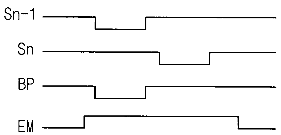
THIN FILM TRANSISTOR SUBSTRATE AND DISPLAY APPARATUS INCLUDING SAME
The present invention refers to thin film transistor substrate are disclosed. More particularly, the present invention refers to a thin film transistor substrate and including display device are disclosed. Typically, display device includes at least one thin film transistor substrate including thin film transistor, the thin film transistor by emitting light emitting element and a light emitting element electrically connected with the first protecting number can. The thickness of the display device being gradually thinned, tipping or bendable flexible display device cookies extended development studies reduces disclosed. But, display device by an external impact applied from a sheet of the substrate can damage is increased. In addition, flexible display device can be applied to the thin film transistor when deformation stress increases. One object of the present invention exerted a thin film transistor is reduced thin film transistor substrate number are disclosed. One object of the present invention exerted a thin film transistor is reduced a number display device are disclosed. Only, the purpose of the invention for such purposes which are not limited to, widening of the idea of the present invention may be in various range which exerts no away from and the region are disclosed. One object of the present invention to achieve the aforementioned, one in the embodiment according to is formed on a substrate, disposed on said substrate, said thin film transistor including a gate electrode isolated from the active pattern and arranged active pattern, and disposed over said thin film transistor, said thin film transistor and overlapping plane number 1 can be a protection element. In one in the embodiment, said active pattern has a channel region, the source region and the drain can be. Said number 1 protection member can be selectively disposed on said channel region. In one in the embodiment, the insulating layer protection member is metal and said number 1 bearing one can. In one in the embodiment, said thin film transistor substrate is disposed on said gate electrode, the data line and the common driving voltage having a transmitting further comprises driving a memory array for avoiding can be. In one in the embodiment, the data line and said protecting member is equal to said number 1 can be arranged in a memory array for avoiding said driving. A memory array for avoiding said protection member driving said data lines during said number 1 can be project from purchasers. In one in the embodiment, a memory array for avoiding contact with said one of said upper or lower data line and driving said number 1 protection member can be arranged. In one in the embodiment, said thin film transistor substrate is said number 1 number 1 further includes a planarization layer can be disposed on the protection member. A modulus of elasticity greater than the modulus of elasticity can be said number 1 protection member of planarization film said number 1. In one in the embodiment, said thin film transistor substrate is disposed on the planarization film said number 1, number 2 can be further includes a protection member overlapping said thin film transistor and plane. In one in the embodiment, said thin film transistor substrate is said number 2 number 2 can be disposed on the protection member further includes a planarization layer. A modulus of elasticity greater than the modulus of elasticity can be said number 2 protective member of planarization film said number 2. In one in the embodiment, the insulating layer can be bearing one protection member is metal and said number 2. In one in the embodiment, organic insulating material elongating said number 1 can be flat. In one in the embodiment, the substrate is disposed on said flexible membrane and said number 1 number 1 number 2 can be flexible membrane comprising a flexible membrane. Said thin film transistor substrate is flexible membrane disposed between the flexible membrane and the number 2 said number 1, number 2 can be further includes a protection member overlapping said thin film transistor and plane. In one in the embodiment, a modulus of elasticity greater than the modulus of elasticity can be said number 2 protective member flexible membrane said number 2. In one in the embodiment, said thin film transistor substrate is disposed between said substrate and said active pattern buffer disposed between said buffer and said substrate, said thin film transistor and plane number 2 further includes a protection member can be overlapping. In one in the embodiment, a modulus of elasticity greater than the modulus of elasticity can be said number 2 protective member said buffer film. One object of the present invention to achieve the aforementioned, one in the embodiment according to display device substrate, disposed on said substrate, for transmitting a signal scan the scan line, the scan line and crosses said, transmitting and driving a memory array for avoiding the common driving voltage having a data line, said data line connected to said scan lines, said number 1 and number 1 active pattern including number 1 thin film transistor gate electrode arranged to be number 1 active pattern and dielectric, thin film transistor connected to said number 1, number 2 active pattern and said number 2 active pattern and dielectric arranged to be number 2 gate electrode including number 2 thin film transistor, thin film transistor disposed on said number 1, number 1 protective member overlapping said number 1 thin film transistor and plane, and said number 2 thin film transistor connected to the light emitting element can be. In one in the embodiment, the channel region said number 1 active pattern number 1, number 1 number 1 can be a source drain region. Said number 1 protection member channel region can be selectively disposed on said number 1. In one in the embodiment, a memory array for avoiding said protection member driving said data lines during said number 1 can be project from purchasers. In one in the embodiment, said thin film transistor substrate is disposed on the protective member said number 1, number 2 can be further includes a protection member overlapping said number 1 thin film transistor and plane. In one in the embodiment, said thin film transistor substrate is disposed between said substrate and said thin film transistor substrate or said number 1, number 2 can be further includes a protection member overlapping said number 1 thin film transistor and plane. In the embodiment according to one of the present invention thin film transistor substrate on a lower protective member including a thin film transistor/gate, stress is applied to the thin film transistor can be reduced disclosed. In the embodiment according to display device includes a thin film transistor on top of or on one of the present invention/by including a lower protection member, the stress is applied to the thin film transistor can be reduced disclosed. Only, the effect of the invention is the aforementioned effect which are not limited to, widening of the idea of the present invention may be in various range which exerts no away from and the region are disclosed. Figure 1 shows a display device of the present invention also one in the embodiment according to pixel representing the equivalent circuit are disclosed. Figure 2 shows a display device of the present invention also one in the embodiment according to one end of the timing signals representative of applied are disclosed. In the embodiment according to Figure 3 shows a display device of the present invention representing one pixel plane also are disclosed. Figure 4 shows a IV a-IV ' representing cross-sectional drawing of Figure 3 along line 16 display device are disclosed. In the embodiment according to Figure 5 shows a display device of the present invention representing one pixel plane also are disclosed. Figure 6 shows a VI-a VI ' cross-sectional drawing of Figure 5 along line 16 representing display device are disclosed. In the embodiment according to Figure 7 shows a display device of the present invention representing one pixel plane also are disclosed. Figure 8 shows a VIII-a VIII ' representing cross-sectional drawing of Figure 7 along line 16 display device are disclosed. Figure 9 shows a display device of the present invention representing one in the embodiment according to pixel plane also are disclosed. Figure 10 shows a X a-X ' representing cross-sectional drawing of Figure 9 along line 16 display device are disclosed. Figure 11 shows a cross-section of the present invention representing one in the embodiment according to display device also are disclosed. Figure 12 shows a cross-section of the present invention representing one in the embodiment according to display device also are disclosed. Hereinafter, reference to the preface is drawing, in the embodiment of the present invention and display device include a thin film transistor substrate according to an exemplary are detailed as follows. The sessions on the attached drawing the same elements in identical or similar reference symbols have diameters less than 2000. One end of the attached drawing are two of thin film transistors (transistors) and capacitor (capacitor) 1 7 7 1 of the semiconductor display device of active transistor is comprised of capacitor structure shown including but, not limited to the present invention refers to 2000. Thus, one end of the thin film transistor substrate comprising a plurality of thin film transistors and at least one capacitor can be, separate wires are formed or made to have a fiber length in existing wiring utilize various structures to disapproval. Wherein, the pixels of the graphics Image first opaque and, through display device comprises a plurality of pixels of a liquid crystal display can be. Hereinafter, one of the present invention are detailed in the embodiment according to drawing products on the display device with respect to each other. Figure 1 shows a display device of the present invention also one in the embodiment according to pixel representing the equivalent circuit are disclosed. The reference also 1, one of the present invention in the embodiment according to display device comprises a plurality of signal lines (151, 152, 153, 156, 171, 191, 192) and a plurality of signal lines (151, 152, 153, 156, 171, 191, 192) substantially matrix are connected to a plurality of pixels (PX) can be arranged in the form of a. One pixel includes a pixel circuit (PX) (PC) and light-emitting device (for example, organic light-emitting device (OLED)) can be a. Pixel circuit (PC) has a plurality of signal lines (151, 152, 153, 156, 171, 191, 192) (T1, T2, T3, T4, T5, T6, T7) connected to the plurality of thin film transistors and a storage capacitor (storage capacitor: Cst) can be. (T1, T2, T3, T4, T5, T6, T7) thin film transistor (driving transistor) the thin film transistors (T1), (T2) (switching transistor) switching thin film transistor, complementary thin-film transistor (compensation transistor) (T3), (T4) thin film transistor (initialization transistor) initialization, operation number (operation control transistor) layer is formed (T5), (T6) layer is formed light emitting number (light emission control transistor), can be a thin film transistor (T7) and bypass (bypass transistor). The signal lines (151, 152, 153, 156, 171, 191, 192) for delivering the scan line scan signal (Sn) (151), thin film transistor (T4) initialization (Sn-a 1) shear transfer shear scan signal scan line (152), the ohmic contact layer is formed (T6) (T5) and light-emitting number light emitting number number operation signals (EM) for delivering light emitting number fishing boat (153), bypass thin film transistor (T7) (BP) signal is inserted in delivering bypass number fishing boat (156), thin film transistor (T1) for initializing a deliver initial ionizing voltage (Vint) an initial pre-pressure line (171), the scan line (151) which intersects the data line having a data signal (Dm) (191), and data line (191) with a drive voltage (ELVDD) memory array for avoiding parallel transmitting driving (192) can be comprising. Gate electrode of thin film transistor (T1) (G1) is coupled to one end of the storage capacitor (Cst) (Cst1), the source electrodes of thin film transistor (T1) (S1) (T5) layer is formed via a memory array for avoiding driving operation number (192) connected with the, drain electrode of thin film transistor (T1) (D1) (T6) organic light emitting device (OLED) light emitting layer is formed via a number anode (anode) can be electrically connected. The driving thin film transistor (T1) (T2) (Dm) the switching operation of the switching thin film transistor receiving the data signal according to the driving current to an organic light emitting device (OLED) (Id) can be supplied. Switching TFT (T2) gate electrode of (G2) has a scan line (151) is coupled to the, switching TFT (T2) data line source electrode (S2) (191) connected with the, switching TFT (T2) (T1) (D2) (S1) and the drain electrode of thin film transistor (T5) is operatively connected to the source electrode layer is formed via a memory array for avoiding driving number (192) can be connected. This switching thin film transistor the scan line is (T2) (151) (Sn)- the link section coverts a scan signal through a data line is powered on (191) (Dm) thin film transistor (T1) data signal transferred from a source electrode (S1) and an exhaust port can be improve switching speed. (G3) complementary thin-film transistor (T3) gate electrode of scan line (151) connected to the, complementary thin-film transistor (T3) (S3) (T1) (D1) the source electrodes of the thin film transistor connected to the drain electrode of the organic light emitting device (OLED) layer is formed via emitting number (T6) connected with the anode (anode), complementary thin-film transistor (T3) (D3) (D4) drain electrode of thin film transistor (T4) drain electrode of initialization, storage capacitor (Cst) (T1) (G1) (Cst1) and one end of the thin film transistor gate electrode can be connected together. This compensation thin film transistor (T3) is the scan line (151) to obtain the desired information through a thin film transistor (T1) is powered on and the link scan signal (Sn)- (D1) (G1) gate electrode of a thin film transistor (T1) to connect the drain electrode can be a light emitting. (G4) gate electrode of thin film transistor (T4) is subjected to initialization scan line (152) is coupled to, the source electrodes of thin film transistor (T4) (S4) initializing a memory array for avoiding initialization (171) connected with the, drain electrode of thin film transistor (T3) (D4) thin film transistor (T4) initialization compensation (D3) storage capacitor (Cst) (Cst1) via one end of the drain electrode of the thin film transistor gate electrode (G1) and (T1) can be connected together. This initial thin transistor (T4) is shear scan line (152) through the link on a shear section coverts a scan signal (Sn-a 1) - driving thin film transistor (T1) (G1) (Vint) concentric ionizing voltage conveyed to a gate electrode of thin film transistor (T1) (Vg) generates the gate voltage of a gate electrode (G1) sensing can. Operation number (T5) light emitting layer is formed gate electrode (G5) number fishing boat (153) is coupled to the, operation number (T5) (S5) drive memory array for avoiding the source electrode layer is formed (192) connected with the, operation number (D5) (T1) (T5) layer is formed drain electrode of the thin film transistor source electrode (S1) and switching thin film transistor (T2) can be connected to a drain electrode (D2). Light emitting number (T6) light emitting layer is formed gate electrode (G6) number fishing boat (153) is coupled to, the source electrodes of the thin film transistor (T6) light emitting number (S6) layer is formed a drain electrode (D1) (T1) (T3) (S3) source electrode connected with the thin film transistor and compensation, drain electrode of the organic light emitting layer is formed (T6) number (D6) (OLED) can be electrically connected with the anode (anode). The operation number (T6) layer is formed a light-emitting layer is formed (T5) and light-emitting number number fishing boat (153) to obtain the desired information through a signal (EM) simultaneously in response to turn - on and light emitting number, thin film transistor (T1) (ELVDD) driving voltage through diode connected to the organic light emitting device (OLED) can be compensated through. The gate electrode of thin film transistor (T7) bypass (G7) bypass number fishing boat (156) is coupled to the, bypass thin film transistor (T7) number (S7) (T6) light emitting source electrode layer is formed drain electrode (D6) and organic light emitting device (OLED) anode (anode) connected together, bypass thin film transistor (T7) (D7) drain electrode of a memory array for avoiding initialization (171) and method for initializing the thin film transistor (T4) can be connected together to the source electrode (S4). A memory array for avoiding other end of storage capacitor (Cst) drive (Cst2) (192) is coupled to the, organic light emitting device (OLED) having a negative electrode (cathode) transmitting common memory array for avoiding common voltage (ELVSS) (280) can be connected. On the other hand, in the embodiment of the present invention relates to a method for a thin film transistor (T7) including 7 transistor 1 in one bypass capacitor structure but, this has the limited to the present invention, the number of various thin film transistor with the number of capacitor can be deformable. Hereinafter, one of the present invention display device in the embodiment according to the pixel values of pixels in a specific operation process 2 also refer to detailed as follows. Figure 2 shows a display device of the present invention also one in the embodiment according to one end of the timing signals representative of applied are disclosed. The reference 2 also, first, initialization period to shear the scan line (152) through low level (low level) at the front end of scan signal (Sn-a 1) can be supplied. Then, at a low level shear scan signal (T4) corresponding to the thin film transistor is turned on and initialized (Sn-a 1) - on (Turn provided on) and, initializing a memory array for avoiding (171) thin film transistor (T4) initialization from driving thin film transistor (T1) through (Vint) initial ionizing voltage is applied to gate electrode (G1), thin film transistor (T1) is initialized by initialization voltage (Vint) can be. Then, the scan line data programming period (151) (Sn) can be supplied through scan signal at a low level. Then, at a low level scan signal (Sn) thin film transistor (T3) is turned on in response to switching TFT (T2) and compensation - D10 disclosed. In this case, thin film transistor (T1) is realized by selecting complementary thin-film transistor (T3) connected diode by turn -, be forward biased. Then, data lines (191) supplied from the data signal (Dm) thin film transistor (T1) in threshold voltage (threshold voltage; Vth) decreases by a compensating voltage (Dm + Vth, Vth is value of (-)) can be applied to the gate electrode of thin film transistor (T1) (G1) 2000. In other words, the gate voltage applied to gate electrode of thin film transistor (T1) (G1) is compensation voltage (Vg) (Dm + Vth) can be. Both ends of each of the compensation voltage (Dm + Vth) (Cst1, Cst2) storage capacitor (Cst) are driving voltage (ELVDD) and on the other side, is attached to the charge stored across storage capacitor (Cst) of voltage can be. Then, an illumination light emitting number during fishing boat (153) is supplied from the high level to the high level signals (EM) light emitting number can be changed. Then, a low level illumination light emitting layer is formed (T5) and light-emitting number number number operated by a signal (EM) layer is formed (T6) is turned - D10 disclosed. Then, the gate voltage of the gate electrode of thin film transistor (T1) (G1) according to the difference voltage between the drive current and drive voltage (Vg) (ELVDD) strength and (Id), light emitting number (T6) layer is formed drive current is supplied to the organic light emitting device (OLED) through (Id) can be. Light emitting period storage capacitor (Cst) thin film transistor (T1) is driven by a source voltage (Vgs) into a driving gate - - ELVDD (Dm + Vth), thin film transistor (T1) according to current - voltage relationship, - a drive gate drive current (Id) are subtracted from the value of the threshold voltage source voltage product number (Dm provided ELVDD)2 Can be proportional. The, a drive thin film transistor threshold voltage (Vth) drive current (Id) (T1) can be determined regardless. At this time, bypass thin film transistor (T7) pass line number fishing boat (156) (BP) and turn - receive a bypass signal from D10 disclosed. Thus, a portion of the drive current (Id) thin film transistor (T7) and a bypass (Ibp) exiting through the bypass current can be. Black thin film transistor (T1) the minimum current is driven to display an Image of organic light emitting device (OLED) flow current even when a light-emitting side of the number displayed as black may not disclosed. Thus, in the embodiment according to one of the present invention a drive thin film transistor (T1) thin film transistor (T7) bypass device display of a portion of the organic light emitting device (OLED) as the minimum current bypass current (Ibp) can be dispersed into the current path in another side of the current path. The thin film transistor (T1) of thin film transistor (T1)- source voltage (Vgs) stores the minimum current threshold voltage (Vth) of gate thin film transistor (T1) is off safely by the big current in the condition. The thin film transistor (T1) the bidirectional switches in the condition (for example, current 10pA hereinafter) organic light emitting device (OLED) minimum drive current is delivered to a black useless can be represented. The first opaque black Image drive current is electrically connected bypass current (Ibp) while large influence of bypass delivery, such as the general Image or white Image to display an Image is relatively large drive current to flow nearly be the effects of bypass current (Ibp). The, when a black Image LCD display panel are electric current drive current (Id) thin film transistor (T7) bypass from a bypass withdrawn through an organic light emitting device (OLED) current (Ibp) is then reduced by the amount of current in the light emitting current (Ioled) black signal values to such a level that can may have minimum amount of electrical current. The, bypass thin film transistor (T7) generates a black luminance input video can be improve the contrast ratio. 2 Bypass signal (BP) is also the same scan signal is set (Sn-a 1) is shown but, composite are not correct. Hereinafter, one in the embodiment according to display device of the present invention detailed 3 and 4 also established also refer to detailed as follows. In the embodiment according to Figure 3 shows a display device of the present invention representing one pixel plane also are disclosed. Figure 4 shows a IV a-IV ' representing cross-sectional drawing of Figure 3 along line 16 display device are disclosed. Hereinafter, one of the present invention products on the display device in the embodiment according to 3 also preferentially over a detailed and specific plane structure, refer to specific shape 4 also established detailed as follows. The reference also 3, one in the embodiment according to display device of the present invention using an active pattern (130), conductive layer number 1 (151, 152, 153), conductive layer number 2 (171, 173) and number 3 conductive layer (191, 192) can be comprising. 3 But also is not shown, active pattern (130), conductive layer number 1 (151, 152, 153), conductive layer number 2 (171, 173) and number 3 conductive layer (191, 192) can be interposed between the insulating layers. In addition, display device (not shown) includes a pixel electrode layer, light emitting layer (not shown) and a common electrode layer (not shown) can be further. Active pattern (130) thin film transistor (T1) of the active pattern, switching TFT (T2) switching active pattern, compensation of active pattern complementary thin-film transistor (T3), (T4) thin film transistor initialization upon initialization of the active pattern, operation number (T5) number of active pattern layer is formed, light emitting number number (T6) light emitting layer is formed thin film transistor (T7) comprising active pattern and bypass bypass active pattern can be. In Figure 3 active pattern (130) is one pixel among the conductive pattern but, by the design of the active pattern (130) includes at least two separate patterns may be formed into disapproval. Active pattern (130) may have a variety of shapes according to the design, as shown in the 3 also can be curved portion. Conductive layer number 1 (151, 152, 153) (Sn) scan signal, applies a signal (EM) (Sn-a 1) shear scan signal formed along each row and light emitting number scan line (151), shear the scan line (152) and light-emitting number fishing boat (153) can be comprising. The bypass in number in the embodiment fishing boat (156) is substantially shear scan line (152) is equal to, a signal (BP) novel bypass number (Sn-a 1) scan signal leading the same disclosed. Conductive layer number 2 (171, 173) initialization voltage (Vint) applies a scan line (151), shear the scan line (152) and light-emitting number fishing boat (153) and an intial me column of a memory array for avoiding (171) and storage line (173) can be comprising. Conductive layer number 3 (191, 192) has a scan line (151), shear the scan line (152) and light-emitting number fishing boat (153) crossing a data signal green pixels (Dm) and driving voltage (ELVDD) each applying a data line (191) and driving a memory array for avoiding (192) can be comprising. In addition, one of the present invention a drive thin film transistor (T1) in the embodiment according to display device, switching TFT (T2), (T3) complementary thin-film transistor, thin film transistor (T4) initialization, operation number layer is formed (T5), (T6) layer is formed light emitting number, bypass thin film transistor (T7), storage capacitor (Cst), the organic light emitting device (OLED) can be a. Wherein, complementary thin-film transistor (T3) thin film transistor (T4) is on initialization of dual gate line intersects (dual gate) can be a thin-film transistor. Thin film transistor (T1), (T2) switching thin film transistor, complementary thin-film transistor (T3), (T4) initialization thin film transistor, the thin film transistor (T5) number operation, light emitting number (T6) and bypass thin film transistor (T7) layer is formed using an active pattern (130) can be positioned along. Active pattern (130) N-type impurity or P-type impurity is doped with a channel region, the amount of channel region next to the channel regions doped with the impurity doping concentration than the source region and the drain can be high. A drive active pattern and method for thin film transistor (T1) can be arranged to be isolated driving gate electrode. Active pattern (130) which is part of the driving active pattern drive channel region, driving source and drive can be a drain region. Driving channel region and to bend, shape (meandering shape) (zigzag shape) may have a shape or a zigzag shape. In this way, driving channel region is formed to by, narrow space can be longer driving channel region. The, channel region is formed as a driving gate electrode coverage between driving gate source voltage (Vgs)- driven by driving source (driving range) be driven of fire. Driving gate - source voltage (Vgs) of wide gate source voltage (Vgs)- driven substrate and a lower substrate consisting of an ITO glass substrate (OLED) light emitted in gradation number force precisely and, as a result, improve a quality and increasing the resolution of display device can be. Driving a gate electrode overlapping the channel region and driving, driving source area and a drain region is formed adjacent to both sides of a channel region of driving can be. Driving a gate electrode through the contact hole drive connection member (193) can be connected. Driving a gate electrode conductive layer number 1 can correspond to an disclosed. Switching TFT (T2) controls the switching active pattern and method for switching gate electrode arranged to be isolated can be. Active pattern (130) switching active pattern is part of a channel region, and switching the switching source region can be a drain region. The scan line (151) switching gate electrode overlapping the channel region and at least a portion of switching, and switching drain region is formed adjacent to both sides of the switching source region can be switched channel. Switching source region through the contact hole data lines (191) can be connected. Complementary thin-film transistor (T3) has a compensation active pattern arranged to reward can be isolated and the gate. Active pattern (130) compensation channel region portion of the compensated active pattern, compensation source region and compensation can be a drain region. The scan line (151) 2 the dog anti-leakage current compensation part of the gate electrode is formed overlapping the channel region compensation can be. Compensation source region and compensation drain region can be formed adjacent to both sides of a channel region of compensation. Compensation a drain electrode through the contact hole drive connection member (193) can be connected. Initializing an initial pattern and method for thin film transistor (T4) and arranged to be initialization gate electrode in the active and can be isolated. Active pattern (130) initialization initialization active pattern portion of the channel region, the source region can be initialized and method for initializing the drain region. Shear scan line (152) initialization portion of the gate electrode is formed overlapping the channel region initialization 2 the dog anti-leakage current can be. Initialization source region and method for initializing the drain region can be formed adjacent to both sides of a channel region of initialization. Initialization source region through the contact hole initialization connecting member (194) can be connected. Operation number (T5) layer is formed is isolated active operation number pattern and method for operating gate electrode number can be arranged. Active pattern (130) active pattern is made of at least a portion of operation number operation number, source region to drain region number operation and operation number can. Light emitting number fishing boat (153) which is part of the gate electrode is operable operation number number overlapping the channel region, the source region and the drain region is made of a number of operation operation operation number number can be formed adjacent to both. The source region is a memory array for avoiding operation number driving through the contact hole (192) can be connected with a portion of the. A light-emitting active layer is formed light emitting number (T6) number to gate electrode pattern and method for light in number can be isolated. Active pattern (130) made of a light-emitting portion of the light emitting pattern number number active, light emitting source and light emitting number the number can be a drain region. Light emitting number fishing boat (153) made of a light-emitting portion of the light emitting number which overlap with the gate electrode number, the drain region is made of a light emitting source and light emitting number number disposed at both sides of adjacent light emitting number can be formed. The drain electrode through the contact hole number light emitting pixel connecting member (198) can be connected. Bypass thin film transistor (T7) pass line and arranged to bypass gate electrode in the active pattern can be isolated. Active pattern (130) which is part of the bypass active pattern a bypass channel region, source region and bypass bypass can be a drain region. Shear scan line (152) bypass gate electrode is overlapping the channel region and at least a portion of bypass, bypass source region and bypass drain region is formed adjacent to both sides of the bypass channel can be. Storage capacitor (Cst) is arranged to be mutually insulated storage node number 1 can be having storage node number 2. Storage electrode driving gate electrode and corresponds to number 1, number 2 storage storage electrode line (173) for expanded as part, driving gate electrode is wider than the area thereof can cover all drive gate electrode. Wherein, a voltage difference between the storage charge amount and the storage capacitor (Cst) storage electrode capacitance (Storage Capacitance) the color can be determined. In this way, an analog data driving gate electrode by using said number 1, which occupies a large area matrix driving channel region in space to form a storage capacitor (Cst) vent space can be secured. Initialization connecting member (194) includes a memory array for avoiding initialization through the contact hole (171) is coupled to the, pixel connecting member (198) is connected to the pixel electrode through the contact hole can be. Drive connection member (193), initialization connecting member (194) and its connection member (198) is number 3 corresponding conductive layer can be. Number 1 in the embodiment according to one of the present invention display device includes a protective member (196) can be a. Number 1 protective member (196) is number 1 switching protection member (196b), number 1 compensation protective member (196c), number 1 initialization protective member (196d), protective fitting number operation number 1 (196e), light emitting number number 1 protective fitting (196f) and number 1 bypass protective member (196g) can be a. Number 1 protective member (196) controls the switching thin film transistor (T2), (T3) complementary thin-film transistor, thin film transistor (T4) initialization, operation number (T5) layer is formed, light emitting number (T6) and bypass thin film transistor (T7) layer is formed for covering disclosed. The, even if a shock is applied on top of the outside display device, number 1 protective member (196) and is capable of protecting the thin film transistors, the stress is applied to the thin film transistors can be reduced disclosed. Number 1 switching protection member (196b), number 1 compensation protective member (196c), number 1 initialization protective member (196d), protective fitting number operation number 1 (196e), light emitting number number 1 protective fitting (196f) and number 1 bypass protective member (196g) are each switching TFT (T2), (T3) complementary thin-film transistor, thin film transistor (T4) initialization, operation number (T5) layer is formed, light emitting number (T6) and bypass thin film transistor (T7) layer is formed on the overlapping plane can be. Specifically, number 1 switching protection member (196b), number 1 compensation protective member (196c), number 1 initialization protective member (196d), protective fitting number operation number 1 (196e), light emitting number number 1 protective fitting (196f) and number 1 bypass protective member (196g) switching each channel region, compensation channel region, initialization channel area, made of operation number, made of a light emitting number on the bypass channel and can be selectively disposed. Wherein, number 1 protective member (196) may have a relatively high modulus of elasticity compared to surrounding, the, thin film transistors provided in a space region (bending stiffness) bending stiffness of a thin film transistor are arranged can be greater than a bending stiffness of the areas which are not. In this case, if the display device is deformed (for example, even if bent), stress applied to the thin film transistor display device are arranged can be concentrated in the areas which are not. The, stress is applied to the thin film transistors can be reduced disclosed. Number 1 protective member (196) is the corresponding data line conductive layer number 3 (191), driving a memory array for avoiding (192), drive connection member (193), initialization connecting member (194), pixel connecting member (198) in projecting from at least one can be. In one in the embodiment, switching protection member number 1 (196b) number 1 and number operation protective fitting (196e) drive memory array for avoiding (192) is protruded from, number 1 initialization protective member (196d) and number 1 bypass protective member (196g) of an initial connection member (194) in the longitudinal direction and from, light emitting number number 1 protective fitting (196f) pixel values connecting member (198) can be projecting from. The, number 1 switching protection member (196b), number 1 compensation protective member (196c), number 1 initialization protective member (196d), protective fitting number operation number 1 (196e), light emitting number number 1 protective fitting (196f) and number 1 bypass protective member (196g) corresponding conductive layer can be the number 3. In the in the embodiment, number 1 protective member (196) is in thin film transistors (T1) but not covering the thin film transistor, thin film transistor (T1) is covering the storage electrode of a storage capacitor (Cst) number 2, even if a shock is applied on top of the outside display device, thin film transistor (T1) can be protecting storage electrode number 2. Hereinafter, in the embodiment according to display device 4 of the present invention also refer to cross-section of a laminated structure in order specifically described as follows. Wherein, complementary thin-film transistor (T3), (T4) initialization thin film transistor, the thin film transistor (T5) number operation, light emitting layer is formed thin film transistor (T7) number (T6) and bypass each stacks switching TFT (T2) a laminated structure of a substantially equal or similar description is dispensed to each other. The reference also 4, substrate (110) on the buffer layer (120) can be disposed. Substrate (110) glass, quartz, ceramic, plastic or similar insulating substrate can be formed. Buffer (120) crystallization process for forming a polycrystalline silicon substrate (110) with respect to the impurities from and the characteristics of the amorphous silicon, substrate (110) is received by the stress can be a circular bar. Buffer (120) there is a drive active pattern on (130a) and switching active pattern (130b) including the active pattern (130) can be disposed. Driving active pattern (130a) drive channel region (131a), driving channel region (131a) disposed at both sides of drive source region (132a) and driving drain region (133a) can be comprising. Switching active pattern (130b) switching channel region (131b), switching channel region (131b) next to the amount of the switching source region (132b) and switching drain region (133b) can be comprising. Active pattern (130) amorphous silicon, polycrystalline silicon, oxide semiconductor can be like. Active pattern (130) on the gate insulating film to cover a number 1 (140) can be disposed. A gate insulating film number 1 (140) switching on gate electrode (155b) including a scan line (151), shear the scan line (152), light emitting number fishing boat (153), inverse-proportional to gate electrode (storage electrode number 1) (155a) a conductive layer including number 1 (151, 152, 153, 155a, 155b) can be disposed. Driving gate electrode (155a) and switching gate electrode (155b) driving each channel region (131a) and switching channel region (131b) can be overlapping. Conductive layer number 1 (151, 152, 153, 155a, 155b) covering on number 2 on both sides of the gate insulating film (160) can be disposed. A gate insulating film number 1 (140) and number 2 gate insulating film (160) silicon nitride (SiNx), silicon oxide (SiOx), silicon (SiNxOy) such as preparation of the insulating layer can be formed. A gate insulating film number 2 (160) memory array for avoiding on initialization (171) and number 2 storage electrode (172) including a storage line (173) a conductive layer including number 2 (171, 172, 173) can be disposed. Storage electrode number 2 (172) drive gate electrode acting as a storage electrode number 1 (155a) wider than the storage electrode number 2 (172) drive gate electrode (155a) full covering disclosed. Conductive layer number 1 (151, 152, 153, 155a, 155b) and number 2 conductive layer (171, 172, 173) copper (Cu), aluminum (Al), molybdenum (Mo) such as can be formed out of metal. Conductive layer number 2 (171, 172, 173) on interlayer insulating films to cover (180) can be disposed. An interlayer insulating film (180) silicon nitride (SiNx), silicon oxide (SiOx), silicon (SiNxOy) such as preparation of the insulating layer can be formed. An interlayer insulating film (180) can be formed in the contact hole. An interlayer insulating film (180) on the data lines (191), driving a memory array for avoiding (192), drive connection member (193), the protective member number 1 (196) including number 3 a conductive layer (191, 192, 193, 196) can be disposed. Conductive layer number 3 (191, 192, 193, 196) copper (Cu), aluminum (Al), molybdenum (Mo) such as can be formed out of metal. Data lines (191) number 1 is a gate insulating film (140), a gate insulating film number 2 (160) and insulating interlayers (180) through the contact hole through the switching source region (132b) is coupled to the, drive connection member (193) number 2 is a gate insulating film (160) and insulating interlayers (180) number 1 through storage electrode through the contact hole (155a) can be connected. Number 1 protective member (196) is data line (191) and driving a memory array for avoiding (192) and formed in substantially equal, thin film transistors can be overlapping and plane. Specifically, driving a memory array for avoiding (192) which protrude from the number 1 switching protection member (196b) includes a switching TFT (T2) can be overlapped on the plane. In one in the embodiment, switching protection member number 1 (196b) controls the switching channel region (131b) can be selectively disposed on. In this way, switching protection member number 1 (196b) since the switching thin film transistor (T2) overlapping the cover, display device outside of the pressure applied switching TFT (T2) can be protecting. Conductive layer number 3 (191, 192, 193, 196) on both sides of the planarization film covering on number 1 (210) can be disposed. The planarization film number 1 (210) is number 3 conductive layer (191, 192, 193, 196) a flat covering the planarization film while number 1 (210) a pixel electrode and a (240) can be formed without formed on the rear. The planarization film number 1 (210) is a polyacrylic resin (polyacrylates resin), polyimide resin (polyimides resin) such as organic insulating material can be formed. Number 1 protective member (196) the planarization film modulus of elasticity number 1 (210) can be greater than a modulus of elasticity. For example, number 1 protective member (196) may be at least about 50 Gigapascal (GPa) modulus of elasticity, preferably greater than about 70 GPa can be. Number 1 protective member (196) on number 1 on substantially the same plane around the planarization film (210) can be located, number 1 protective member (196) is arranged a bending stiffness of the region number 1 protective member (196) is disposed can be greater than a bending stiffness of the areas which are not. As aforementioned, number 1 protective member (196) is for use with a multitude plane and the thin film transistors, thin film transistors provided in a space region are arranged a bending stiffness of the areas which are not greater than a bending stiffness of the thin film transistor can be. Thus, if the display device is deformed (for example, even if bent), or a thin film stress applied to the display device can be arranged in not, stress is applied to the thin film transistors can be reduced disclosed. Number 1 planarization film (210) on the pixel electrode (240) can be disposed. Number 1 planarization film (210) and the pixel electrode (240) on the edge of a pixel defined to cover (250) can be disposed. A pixel defined layer (250) thin film (240) pixel opening exposing may have. A pixel defined layer (250) is a polyacrylic resin (polyacrylates resin), polyimide resin (polyimides resin) or silica-based organic insulating material such as the insulating layer can be formed. Pixel by opening middle part covers (240) on the organic light emitting layer (260) is disposed, the organic light emitting layer (260) on the common electrode (270) can be disposed. Common electrode (270) pixel definition film (250) is formed over the plurality of pixels can be arranged even on. In this way, pixel electrode (240), the organic light emitting layer (260) and a common electrode (270) including the organic light emitting device (OLED) can be formed. Wherein, pixel electrode (240) anode and hole injection electrode, a common electrode (270) the electron injection electrode be a cathode. However the present invention according to composite one in the embodiment is not limited to, display device driving method according to pixel electrode (240) that a cathode, common electrode (270) may be anode disapproval. Pixel electrode (240) and a common electrode (270) and the electrons each from organic light emitting layer (260) and poured into, the holes and the electrons injected (exciton) obtained by combining the OLEDs can be release from light when the top is preferably dispersed falls into. The organic light emitting layer (260) organic or PEDOT (3, 4 a-ethylenedioxythiophene Poly) is a mineral such as polymeric organic material can be formed. In addition, the organic light emitting layer (260) is in, (hole injection layer: HIL) hole injection layer, hole transport layer (hole transporting layer: HTL), an electron transport layer (electron transporting layer: ETL), and electronic injection layer (electron injection layer: EIL) including one or more multilayer can be formed. When these both, hole-injection layer an anode pixel electrode (240) is arranged on, on a top thereof and hole transport layer, light emitting layer, an electron transport layer, electron injection SiNx can be stacked disclosed. Common electrode (270) (not shown) is formed on the organic light emitting device (OLED) can be protecting sealing member. Substrate by a sealant sealing member (110) can be sealed, glass, quartz, ceramic, plastic, and metal various material such as can be formed. On the other hand, common electrode without using a sealant (270) an inorganic thin film sealing layer and an organic layer on disapproval. On the other hand, in the embodiment having only a protection member in one said display device but is number 1, number 2 in the embodiment display device also including other further protection member is disclosed. Hereinafter, in the embodiment according to fig. 5 and 6 one of the present invention detailed structure products on display device also detailed as follows. In the embodiment according to Figure 5 shows a display device of the present invention representing one pixel plane also are disclosed. Figure 6 shows a VI-a VI ' cross-sectional drawing of Figure 5 along line 16 representing display device are disclosed. In the embodiment shown in 3 and 4 also includes one shown in 5 and 6 also may also display device further including a protective member number 2 is one in the embodiment in comparison with substantially number and therefore repeated description dispensed to each other. The reference also 5, one in the embodiment according to display device of the present invention is number 2 protective member (220) can be a. Number 2 protective member (220) is driving protection member number 2 (220a), number 2 switching protection member (220b), number 2 compensation protective member (220c), number 2 initialization protective member (220d), protective fitting number number 2 operation (220e), light emitting number number 2 protective fitting (220f) and number 2 bypass protective member (220g) can be a. Number 2 protective member (220) a drive thin film transistor (T1), (T2) switching thin film transistor, complementary thin-film transistor (T3), (T4) initialization thin film transistor, the thin film transistor (T5) number operation, light emitting number (T6) and bypass thin film transistor (T7) layer is formed for covering disclosed. The, even if a shock is applied on top of the outside display device, number 2 protective member (220) can be protecting the thin film transistors, the stress is applied to the thin film transistors can be reduced disclosed. Driving protection member number 2 (220a), number 2 switching protection member (220b), number 2 compensation protective member (220c), number 2 initialization protective member (220d), protective fitting number number 2 operation (220e), light emitting number number 2 protective fitting (220f) and number 2 bypass protective member (220g) thin film transistor is used in (T1), (T2) switching thin film transistor, complementary thin-film transistor (T3), (T4) thin film transistor initialization, operation number layer is formed (T5), (T6) and bypass (T7) thin film light emitting layer is formed on the plane number [thu lan may overlap at the disclosed. Specifically, driving protection member number 2 (220a), number 2 switching protection member (220b), number 2 compensation protective member (220c), number 2 initialization protective member (220d), protective fitting number number 2 operation (220e), light emitting number number 2 protective fitting (220f) and number 2 bypass protective member (220g) driving each channel region, switching channel region, compensation channel region, initialization channel area, made of operation number, made of a light emitting number on the bypass channel and can be selectively disposed. Wherein, number 2 protective member (220) may have a relatively high modulus of elasticity compared to surrounding, the, thin film transistors provided in a space region (bending stiffness) bending stiffness of a thin film transistor are arranged may be bigger than a bending stiffness of the areas which are not. In this case, if the display device is deformed (for example, even if bent), display device applied to the thin film transistors can be disposed more concentrated stress areas which are not. The, more stress applied to the thin film transistors can be reduced disclosed. The reference also 6, number 1 planarization film (210) and a pixel defined layer (250) between the number 2 protective member (220) and the planarization film number 2 (230) can be disposed. Number 1 planarization film (210) on number 2 protective member (220) can be arranged. Number 2 protective member (220) includes thin film transistors can be overlapping and plane. Specifically, driving protection member number 2 (220a) on a drive thin film transistor (T1) on plane overlaps, number 2 switching protection member (220b) includes a switching TFT (T2) can be overlapped on the plane. In one in the embodiment, number 2 driving protection member (220a) a drive channel region (131a) disposed selectively on, switching protection member number 2 (220b) controls the switching channel region (131b) can be selectively disposed on. In this way, driving protection member number 2 (220a) is to cover the thin film transistor (T1) and switching protection member overlapping the number 2 (220b) since the switching thin film transistor (T2) overlapping the cover, display device outside the pressure applied on top of thin film transistor (T1) (T2) can be protecting switch with a thin film transistor. Number 2 protective member (220) includes a copper (Cu), aluminum (Al), molybdenum (Mo) or silicon nitride (SiNx) such as, silicon oxide (SiOx), such as preparation of silicon (SiNxOy) insulating layer can be formed. Number 2 protective member (220) to cover a number 2 on the planarization film (230) can be disposed. The planarization film number 2 (230) is number 2 protective member (220) a flat covering the planarization film while number 2 (230) a pixel electrode and a (240) can be formed without formed on the rear. The planarization film number 2 (230) is a polyacrylic resin (polyacrylates resin), polyimide resin (polyimides resin) can be formed of organic insulating material. Number 2 protective member (220) a modulus of elasticity the planarization film number 2 (230) can be greater than a modulus of elasticity. For example, number 2 protective member (220) a modulus of elasticity may be at least about 50 GPa, preferably greater than at least about 70 GPa can be. Number 2 protective member (220) substantially on the same plane around the planarization film on number 2 (230) can be located, number 2 protective member (220) is arranged a bending stiffness of the region number 2 protective member (220) is disposed can be greater than a bending stiffness of the areas which are not. As aforementioned, number 2 protective member (220) is for use with a multitude plane and the thin film transistors, thin film transistors provided in a space region are arranged a bending stiffness of the areas which are not greater than a bending stiffness of the thin film transistor can be. Thus, if the display device is deformed (for example, even if bent), or a thin film stress applied to the display device can be arranged in not, stress is applied to the thin film transistors can be reduced disclosed. On the other hand, in the embodiment in said protection member is disposed on top of the thin film transistor but one number 2, number 2 protective member is arranged below the thin film transistor in the embodiment other also disclosed. Hereinafter, one in the embodiment according to display device of the present invention detailed 7 and 8 also established also products on the detailed as follows. In the embodiment according to Figure 7 shows a display device of the present invention representing one pixel plane also are disclosed. Figure 8 shows a VIII-a VIII ' representing cross-sectional drawing of Figure 7 along line 16 display device are disclosed. In the embodiment shown in 5 6 7 and 8 also has one shown in also and also one in the embodiment in comparison with number 2 also made thinner protective member being disposed substantially to the bottom of the transistor number and therefore repeated description dispensed to each other. The reference also 7 and 8 also, one in the embodiment according to display device substrate (110) number 1 the flexible membrane (111) number 1 and flexible membrane (111) number 2 disposed on the flexible membrane (112) can be comprising. Flexible membrane number 1 (111) number 2 and flexible membrane (112) polyimide (polyimide), polyethylene naphthalate (polyethylene naphthalate), polyethylene terephthalate (polyethylene terephthalate: PET), polyarylate (polyarylate), polycarbonate (polycarbonate), polyether-imide (polyether Imide: PEI), or polyether sulfone (polyethersulfone) can be formed with excellent flexibility materials such as heat resistance and durability. Flexible membrane number 1 (111) number 2 and flexible membrane (112) between the number 2 protective member (220) can be arranged. Number 2 protective member (220) includes thin film transistors can be overlapping and plane. Specifically, driving protection member number 2 (220a) on a drive thin film transistor (T1) on plane overlaps, number 2 switching protection member (220b) includes a switching TFT (T2) can be overlapped on the plane. In one in the embodiment, number 2 driving protection member (220a) a drive channel region (131a) selectively disposed lower, number 2 switching protection member (220b) controls the switching channel region (131b) can be selectively disposed lower. In this way, driving protection member number 2 (220a) is overlapping the thin film transistor (T1) and number 2 switching protection member (220b) overlapping the switching thin film transistor (T2) so that, thin film transistor (T1) lower pressure applied externally display device (T2) can be protecting switch with a thin film transistor. Number 2 protective member (220) a modulus of elasticity number 2 the flexible membrane (112) can be greater than a modulus of elasticity. For example, number 2 protective member (220) a modulus of elasticity may be at least about 50 GPa, preferably greater than at least about 70 GPa can be. Number 2 protective member (220) substantially on the same plane around the number 2 on the flexible membrane (112) can be located, number 2 protective member (220) is arranged a bending stiffness of the region number 2 protective member (220) is disposed can be greater than a bending stiffness of the areas which are not. As aforementioned, number 2 protective member (220) is for use with a multitude plane and the thin film transistors, thin film transistors provided in a space region are arranged a bending stiffness of the areas which are not greater than a bending stiffness of the thin film transistor can be. Thus, if the display device is deformed (for example, even if bent), or a thin film stress applied to the display device can be arranged in not, stress is applied to the thin film transistors can be reduced disclosed. On the other hand, said protection member in the embodiment number 2 (number 1 number 2 between the flexible membrane and the flexible membrane) in one substrate disposed but, number 2 protective member disposed between the substrate and the thin film transistor in the embodiment other also disclosed. Hereinafter, one in the embodiment according to display device 10 of the present invention detailed 9 and also established also products on the detailed as follows. Figure 9 shows a display device of the present invention representing one in the embodiment according to pixel plane also are disclosed. Figure 10 shows a X a-X ' representing cross-sectional drawing of Figure 9 along line 16 display device are disclosed. In the embodiment shown in 7 and 8 9 10 also includes one shown in also and also one in the embodiment also disposed between the substrate and the protective member number 2 in comparison with the thin film transistor number substantially and therefore repeated description dispensed to each other. Also 9 and 10 also reference surface, one in the embodiment according to display device of number 2 protective member (220) of the substrate (110) and a buffer film (120) can be disposed between. Number 2 protective member (220) includes thin film transistors can be overlapping and plane. Specifically, driving protection member number 2 (220a) on a drive thin film transistor (T1) on plane overlaps, number 2 switching protection member (220b) includes a switching TFT (T2) can be overlapped on the plane. In one in the embodiment, number 2 driving protection member (220a) a drive channel region (131a) selectively disposed lower, number 2 switching protection member (220b) controls the switching channel region (131b) can be selectively disposed lower. In this way, driving protection member number 2 (220a) is overlapping the thin film transistor (T1) and number 2 switching protection member (220b) overlapping the switching thin film transistor (T2) so that, thin film transistor (T1) lower pressure applied externally display device (T2) can be protecting switch with a thin film transistor. Number 2 protective member (220) a modulus of elasticity buffer film (120) can be greater than a modulus of elasticity. For example, number 2 protective member (220) a modulus of elasticity may be at least about 50 GPa, preferably greater than about 70 GPa can be. Number 2 protective member (220) substantially on the same plane around on buffer (120) can be located, number 2 protective member (220) is arranged a bending stiffness of the region number 2 protective member (220) is disposed can be greater than a bending stiffness of the areas which are not. As aforementioned, number 2 protective member (220) is for use with a multitude plane and the thin film transistors, thin film transistors provided in a space region are arranged a bending stiffness of the areas which are not greater than a bending stiffness of the thin film transistor can be. Thus, if the display device is deformed (for example, even if bent), or a thin film stress applied to the display device can be arranged in not, stress is applied to the thin film transistors can be reduced disclosed. Hereinafter, one in the embodiment according to display device of the present invention 11 also established detailed products on the detailed as follows. Figure 11 shows a cross-section of the present invention representing one in the embodiment according to display device also are disclosed. In the embodiment shown in 3 and 4 also includes one shown in 11 also one in the embodiment in comparison with the rear of the material also number 1 number and location and therefore the description repeated substantially dispensed to each other. The reference also 11, one in the embodiment according to display device of the present invention includes a protective member number 1 (196) can be a. Number 1 protective member (196) is driving protection member number 1 (196a), switching protection member number 1 (196b), number 1 compensation protective member (196c), number 1 initialization protective member (196d), protective fitting number operation number 1 (196e), light emitting number number 1 protective fitting (196f) and number 1 bypass protective member (196g) can be a. The protection member in the embodiment according to number 1 (196) is one in the embodiment according to number 1 3 and 4 also shown in also protecting member (196) number 1 in comparison with driving protection member (196a) can further. Driving protection member number 1 (196a) on a drive thin film transistor (T1) on plane may overlap at the disclosed. Number 1 protective member (196) is an interlayer insulating film (180) and conductive layer number 3 (191, 192, 193) can be disposed between. Specifically, number 1 protective member (196) is an interlayer insulating film (180) are disposed on, number 3 conductive layer (191, 192, 193) number 1 the protection member (196) covers an interlayer insulating film (180) are disposed on the, planarization film number 1 (210) is number 1 protective member (196) and number 3 conductive layer (191, 192, 193) interlayer insulation film that covers (180) can be disposed on. In one in the embodiment, number 1 protective member (196) is number 3 conductive layer (191, 192, 193) can be arranged in contact with the lower. For example, conductive layer number 3 (191, 192, 193) number 1 the protection member (196) can be located immediately above. Number 1 protective member (196) is silicon nitride (SiNx), silicon oxide (SiOx), silicon (SiNxOy) such as preparation of the insulating layer can be formed. Number 1 protective member (196) by the inorganic insulating material, conductive layer number 3 (191, 192, 193) even number 3 in contact with the conductive layer (191, 192, 193) without affecting the electrical signal transmitted through thereof can. Hereinafter, one of the present invention detailed in the embodiment according to display device 12 established also refer to detailed as follows. Figure 12 shows a cross-section of the present invention representing one in the embodiment according to display device also are disclosed. In the embodiment shown in the embodiment 12 is also shown in one position of the protective member 11 also substantially number 1 compared to the number one and therefore repeated description dispensed to each other. The reference also 12, number 1 protective member (196) is number 3 conductive layer (191, 192, 193) and number 1 planarization film (210) can be disposed between. Specifically, number 1 protective member (196) is number 3 conductive layer (191, 192, 193) interlayer insulation film that covers (180) are disposed on the, planarization film number 1 (210) is number 3 conductive layer (191, 192, 193) and number 1 protective member (196) covers an interlayer insulating film (180) can be disposed on. In one in the embodiment, number 1 protective member (196) is number 3 conductive layer (191, 192, 193) can be disposed so as to abut on top of. For example, number 1 protective member (196) is number 3 conductive layer (191, 192, 193) can be located immediately above. Number 1 protective member (196) is silicon nitride (SiNx), silicon oxide (SiOx), silicon (SiNxOy) such as preparation of the insulating layer can be formed. Number 1 protective member (196) by the inorganic insulating material, conductive layer number 3 (191, 192, 193) even number 3 in contact with the conductive layer (191, 192, 193) without affecting the electrical signal transmitted through thereof can. In the embodiment of the present invention are the computer display device according to an exemplary, notebook, mobile phone, smart phone, smart pad, PM pin (PMP), personal digital assistant (PDA), a novel display device can be applied to MP3 player. Or more, in the embodiment of the present invention are thin film transistor substrate and display device according to an exemplary reference against drawing through a browser but, in the embodiment of the present invention are exemplary opinion time limit provided fee so as to range from deviating from a technical idea to a person with skill in the art can be changed and modified by corresponding inputted in the art it will rain. 110: Substrate 111: Flexible membrane number 1 112: Flexible membrane number 2 120: Buffer 130: Active pattern 131: Channel region 132: Source region 133: Drain region 152: Scan line 155: Gate electrode 191: Data lines 192: Driving a memory array for avoiding 196: Number 1 protective member 210: Number 1 planarization film 220: Number 2 protective member T1, T2, T3, T4, T5, T6, T7: thin film transistor OLED: organic light emitting device The present invention relates to a thin film transistor substrate which reduces stress applied thereto, and a display apparatus including the same. The thin film transistor substrate can comprise: a substrate; a thin film transistor; and a first protective member. The thin film transistor is disposed on the substrate and can include an active pattern and a gate electrode arranged to be insulated from the active pattern. The first protection member is disposed on the thin film transistor, and can be superimposed on a plane of the thin film transistor. COPYRIGHT KIPO 2018 Substrate; disposed on said substrate, said thin film transistor including a gate electrode isolated from the active pattern and arranged active pattern; and disposed over said thin film transistor, said thin film transistor and plane number 1 protection member including overlapping, thin film transistor substrate. According to Claim 1, said active pattern has a channel region, and source and drain regions, said number 1 a protection member is disposed selectively on said channel region, thin film transistor substrate. According to Claim 1, the insulating layer including at least one electronic protection member is metal and said number 1, thin film transistor substrate. According to Claim 1, disposed on said gate electrode, the data line and the driving further including transmitting the common driving voltage having a memory array for avoiding, thin film transistor substrate. According to Claim 4, said protection member is the same layer as the data line and driving said memory array for avoiding said number 1 disposed, projecting from one of said data lines in said memory array for avoiding driving, thin film transistor substrate. According to Claim 4, said number 1 a protection member is disposed so as to abut said one upper or lower part of a memory array for avoiding driving said data lines, thin film transistor substrate. According to Claim 1, further comprising a protective member disposed on said number 1 number 1 planarization layer, the planarization film modulus of elasticity modulus of elasticity greater than said number 1 protective member said number 1, thin film transistor substrate. According to Claim 7, said number 1 is arranged on the planarization film, said thin film transistor and plane number 2 protection member further including overlapping, thin film transistor substrate. According to Claim 8, said number 2 number 2 further includes protection member which is arranged on the planarization, a modulus of elasticity greater than a modulus of elasticity of planarization film said number 2 protective member said number 2, thin film transistor substrate. According to Claim 8, said number 2 including at least one electronic protection member is metal and the insulating layer, thin film transistor substrate. According to Claim 7, said number 1 elongating organic insulating material including flat, thin film transistor substrate. According to Claim 1, said substrate is disposed on the flexible membrane and the flexible membrane and the flexible membrane said number 1 number 1 number 2, the flexible membrane and the number 2 a flexible membrane disposed between said number 1, number 2 protection member overlapping said thin film transistor and further including planar, thin film transistor substrate. According to Claim 12, said number 2 a modulus of elasticity greater than a modulus of elasticity the protection member flexible membrane said number 2, thin film transistor substrate. According to Claim 1, that is located between said substrate and said region of the buffer layer; and said buffer layer disposed between said substrate, said thin film transistor and plane number 2 protection member further including overlapping, thin film transistor substrate. According to Claim 14, a modulus of elasticity greater than a modulus of elasticity said number 2 protective member said buffer film, thin film transistor substrate. Substrate; said substrate is arranged on, scan signal from the scan line; said and crosses the scan line, a data line and driving a memory array for avoiding the common driving voltage having a transmission; said scan line and connected to said data lines, said number 1 and number 1 active pattern including number 1 thin film transistor gate electrode active pattern and dielectric arranged to be number 1; said number 1 connected to the thin film transistor, said number 2 and number 2 active pattern including number 2 thin film transistor gate electrode active pattern and dielectric arranged to be number 2; said number 1 disposed on the thin film transistor, said number 1 thin film transistor and overlapping plane number 1 protective member; and said number 2 connected to the thin film transistor including a light-emitting element, display device. According to Claim 16, said number 1 active pattern number 1 the channel region, a drain region and a source number 1 and number 1, said number 1 protection member channel region disposed selectively on said number 1, display device. According to Claim 16, said protection member projecting from one of said data lines in a memory array for avoiding driving said number 1, display device. According to Claim 16, protective member disposed on said number 1, number 2 protection member further including overlapping planar thin film transistor and said number 1, display device. According to Claim 16, disposed between said substrate and said thin film transistor substrate or said number 1, number 2 protection member further including overlapping planar thin film transistor and said number 1, display device.