RESONANCE ENHANCED ABSORPTIVE COLOR FILTERS
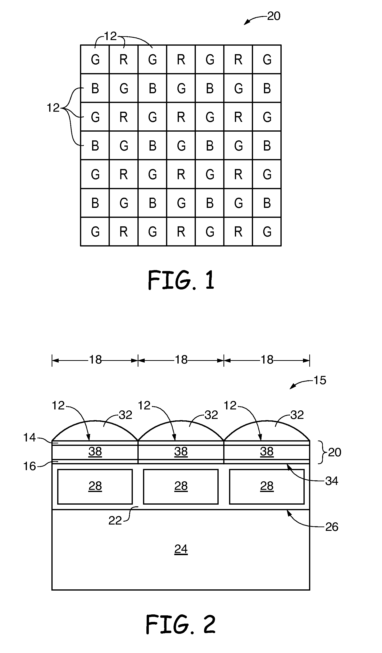
This application claims the benefit of provisional patent application No. 61/557,345, filed Nov. 8, 2011 which is hereby incorporated by reference herein in its entirety. This relates generally to imaging devices, and more particularly, image sensors having resonance enhanced absorptive color filters for both back and front side illumination image sensors. Image sensors are commonly used in electronic devices such as cellular telephones, cameras, and computers to capture images. Conventional image sensors are fabricated on a semiconductor substrate using complementary metal-oxide-semiconductor (CMOS) technology or charge-coupled device (CCD) technology. An image sensor may include an active pixel array having photodiodes. A color filler array is often formed over the photodiodes. The color fitter array contains color filters such as red, green, and blue color filters that filter incoming light before it reaches the photodiodes. However, conventional color filter arrays may be susceptible to optical cross talk. It would therefore be desirable to be able to provide improved color filter arrays for image sensors. Digital camera modules are widely used in electronic devices such as digital cameras, computers, cellular telephones, or other electronic devices. These electronic devices may include image sensors that receive incoming light to capture an image. The image sensors may include arrays of image sensor pixels. The pixels in the image sensors may include photosensitive elements such as photodiodes that convert the incoming light into digital data. Image sensors may have any number of pixels (e.g., hundreds or thousands or more). A typical image sensor may, for example, have millions of pixels (e.g., megapixels). In high-end equipment, image sensors with ten megapixels or more are not uncommon. Image sensors in digital cameras and other digital imaging devices typically have an array of pixels. Each pixel may have an associated color filter of for example, red, green, or blue. Color filter array 20 of In a resonance cavity, incoming light forms a standing wave between two reflectors. One or both of the reflectors may be only partially reflective in order to allow incoming light to enter or leave the resonance cavity. Each resonance enhanced color filter 12 in color filter array 20 may serve as a resonance cavity. The resonance cavity may be an absorptive resonance cavity. Multiple passes of light within the resonance cavity may result in absorptive side bands. For a green color filter, green light may be transmitted while red and blue light may be absorbed in absorption side bands. For a red color filter, red light may be transmitted while blue and green light may be absorbed. For a blue color filter, blue light may be transmitted while red and green light may be absorbed. Absorbed light may generate electrons and holes within the color filter material. A depletion region may form within the color filter material. Interfaces between the color filter material and adjacent layers may form opposing partially reflective interfaces for a resonance cavity. Partial reflectors and reflective interfaces may be made based on 1) Fresnel index contract reflections between different semiconductor materials; 2) Additional semiconductor material layers(s); 3) Plasmon-based 3D structures 4) Photonic band gap filter structures; 5) geometrically set up resonators; or 6) a combination of any of 1-5 with absorption filters. A cross-sectional side view of an illustrative back side illumination (BSI) image sensor that may have resonance enhanced color filter arrays is shown in Each pixel 18 has a photodiode 28 formed in a front side 26 of silicon substrate 48. A resonance enhanced color filter array 20 may be formed on back surface 34 of substrate 22. Microlenses 32 may be formed in an array over color filter array 20. Light can enter from the back side of the image sensor pixels through microlenses 32. Photons incident on photodiodes 28 may be converted into charge that is output as pixel signals. Resonance enhanced color filters 12 in color filter array 20 may have color filter material 38. A resonance cavity may be formed in each color filter 12. A resonance cavity may be formed in color filter material 38 between interfaces between color filter 38 and adjacent materials. A layer 14 may be provided between color filter material 38 and microlenses 32. Layer 14 may serve as a partially reflecting interface for a resonance cavity. Alternatively, an interface between layer 14 and color filter material 25 may serve as a partially reflecting interface for a resonance cavity. Layer 14 may be a material with a higher refractive index than color filter material 38. Layer 14 may have a refractive index in a range of 1.4 to 4.5, over 2.0, or in another suitable range. Layer 14 may be a high refractive index material such as silicon, silicon oxide, silicon nitride, silicon carbide, titanium oxide, tin oxide, germanium, or other suitable materials. Color filter material may have a refractive index of about 1.6, or in a range of 1.0 to 2.0. An interface between a high refractive index material 14 and color filter material 38 may serve as a partially reflecting interface for a resonance cavity. If desired, layer 14 may be formed from a metamaterial. A metamaterial layer may have features of about 100-200 nm in size. Layer 14 may be a plasmonic metamaterial or a bandgap metamaterial. A plasmonic metamaterial may have metal embedded in a dielectric. A bandgap metamaterial may have two alternating dielectrics. Types of metal that may be used in a plasmonic metamaterial include aluminum, copper, silver, titanium, tungsten, or other suitable metals. Types of dielectrics that may be used for plasmonic or bandgap metamaterials include silicon, silicon oxide, silicon, nitride, silicon carbide, titanium oxide, tin oxide, germanium, or other suitable dielectrics. A layer 16 may be provided between color filter material 38 and substrate 22. A partially reflective interface may be formed between color filter material 38 and substrate 22. Layer 16 may be a high refractive index material or a metamaterial. Alternatively, layer 16 may be omitted and an interface between color filter material 18 and substrate 22 may serve as a partially reflecting interface for the resonance cavity. If desired, layer 16 may be included in resonance enhanced color filter 12 and layer 14 omitted. If layer 14 is omitted, an interface between color filter material 38 and microlenses 32 may serve as a partially reflecting interlace for a resonance cavity. Resonance enhanced color filters 12 may be made thinner than conventional color filters. It may be advantageous to have thinner color filters in order to better handle incident light having chief ray angles that are off from vertical. Resonance enhanced color filter 12 may have a thickness of e.g., about 200 nm, 150-250 nm, less than 300 nm, or other suitable thicknesses. A resonance color filter array 20 may have a uniform thickness. If desired, a resonance enhanced color filler array 20 may be formed having color filters 12 with different thickness for different colors. Back side illumination sensors may also be provided with color filter material on a front side 26 of a substrate as well as on a back side 34 of a substrate (see, e.g., Processor system 300, which may be a digital still or video camera system, may include a lens such as lens 396 for focusing an image onto a pixel array such as pixel array 201 when shutter release button 397 is pressed. Pixel array 201 may resonance enhanced color filter array of Various embodiments have been described illustrating resonance enhanced color filter arrays. Resonance enhanced color filter arrays are provided tor image sensors. Resonance cavities are formed with color filter materials that enhance the color filtering capabilities of the color filter materials. Resonance enhanced color filter arrays may be provided for back side illumination image sensors. A layer of high refractive index material or metamaterial may be provided between a microlens and a color filter material to serve as a first partially reflecting interface for the resonance cavity. An optional layer of high refractive index material or metamaterial may be provided between color filter material and a substrate. Resonance enhanced color filter arrays may be provided for front side illumination image sensors. Front side illumination image sensors may have a light guide structure formed in interlayer dielectric that guides light to photodiodes in a substrate. Color filter material may be provided in a light guide structure. The color filter material in the light guide structure may form at least part of a resonance cavity for a resonance enhanced color filter array. A color filter array layer may also be provided that together forms a resonance cavity with the light guide structure. Back side illumination sensors may also be provided with color filter material on a front side of a substrate as well as on a back side of a substrate. Color filter material on a front side of a substrate may form a resonance cavity together with a substrate layer and color filter material on a back side of a substrate. If desired, color filter material on a front side of substrate may form a resonance cavity together with a substrate layer, and color filter material on a back side of the substrate may be omitted. The foregoing is merely illustrative of the principles of this invention which can be practiced in other embodiments. Resonance enhanced color filter arrays are provided for image sensors. Resonance cavities formed with color filter materials that enhance the color filtering capabilities of the color filter materials. Resonance enhanced color filter arrays may be provided for back side illumination image sensors and front side illumination image sensors. A layer of high refractive index material or metamaterial may be provided between a microlens and a color filter material to serve as a first, partially reflecting interface for the resonance cavity. An optional layer of high refractive index material or metamaterial may be provided between color filter material and a substrate. In front side illumination image sensors, color filter material may be provided in a light guide structure that extends through interlayer dielectric. The color filter material in the light guide structure may form at least part of a resonance cavity tor a resonance enhanced color filter array. 1. An image sensor, comprising:
an array of photodiodes in a substrate; color filter material in a color filter array; and first and second interfaces that form a resonance cavity with the color filter material, wherein the resonance cavity enhances a color filtering capability of the color filter material. 2. The image sensor defined in a micro lens array; and a layer of material between the microlens array and the color filter material, wherein the first interface comprises a partially-reflecting interface between the layer of material and the color filter material. 3. The image sensor defined in 4. The image sensor defined in 5. The image sensor defined in 6. The image sensor defined in a light guide cavity in an interlayer dielectric between the color filter array and the substrate, wherein the light guide cavity is at least partially filled with color filter material, and wherein the light guide cavity forms a portion of the resonance cavity. 7. The image sensor defined in an additional layer of material between the color filter material and the substrate, wherein the second interface comprises a partially-reflecting interface between the additional layer of material and the color filter material. 8. The image sensor defined in 9. An image sensor, comprising;
an array of photodiodes in a substrate; color filter material in a color filter array; a microlens array; and a metamaterial layer between the color fitter material and the microlens array, wherein a resonance cavity is formed at least partly from the color filter material and a first partially-reflecting interface between the color filter material and the metamaterial layer. 10. The image sensor defined in 11. The image sensor defined in 12. The linage sensor defined in 13. The image sensor defined in 14. The image sensor defined in 15. The image sensor defined in 16. A system, comprising:
a central processing unit; memory; input-output circuitry; and an imaging device, wherein the imaging device comprises:
a pixel array in a substrate; and a resonance enhanced color filter array, wherein the color filter array forms at least part of a resonance cavity. 17. The system defined in color filter material; and a patterned 3D band gap filter in the color filter material. 18. The system defined in 19. The system defined in 20. The system defined in BACKGROUND
BRIEF DESCRIPTION OF THE DRAWINGS
DETAILED DESCRIPTION