METHOD OF MANUFACTURING DETECTION DEVICE, DETECTION DEVICE, AND DETECTION SYSTEM
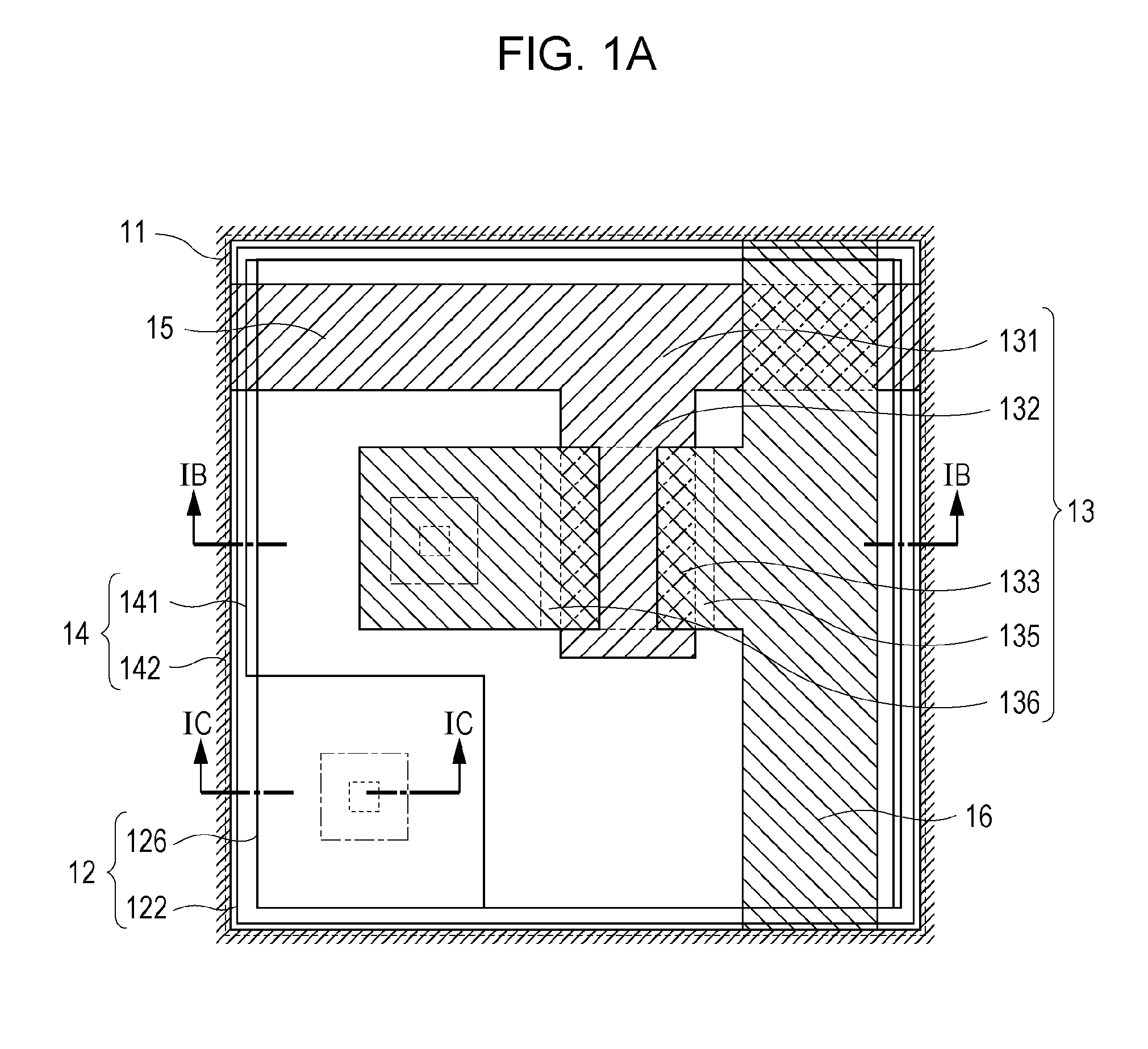
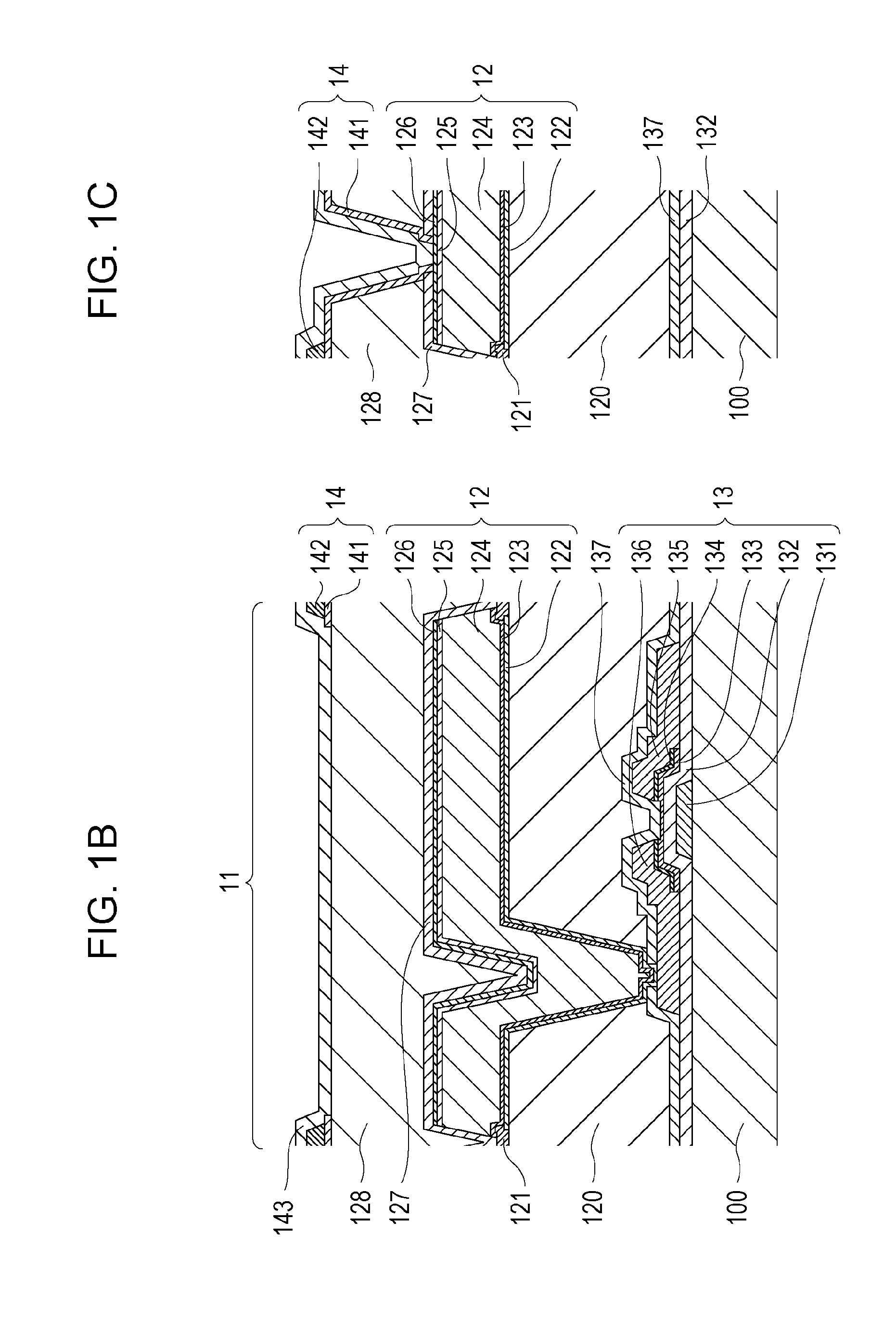
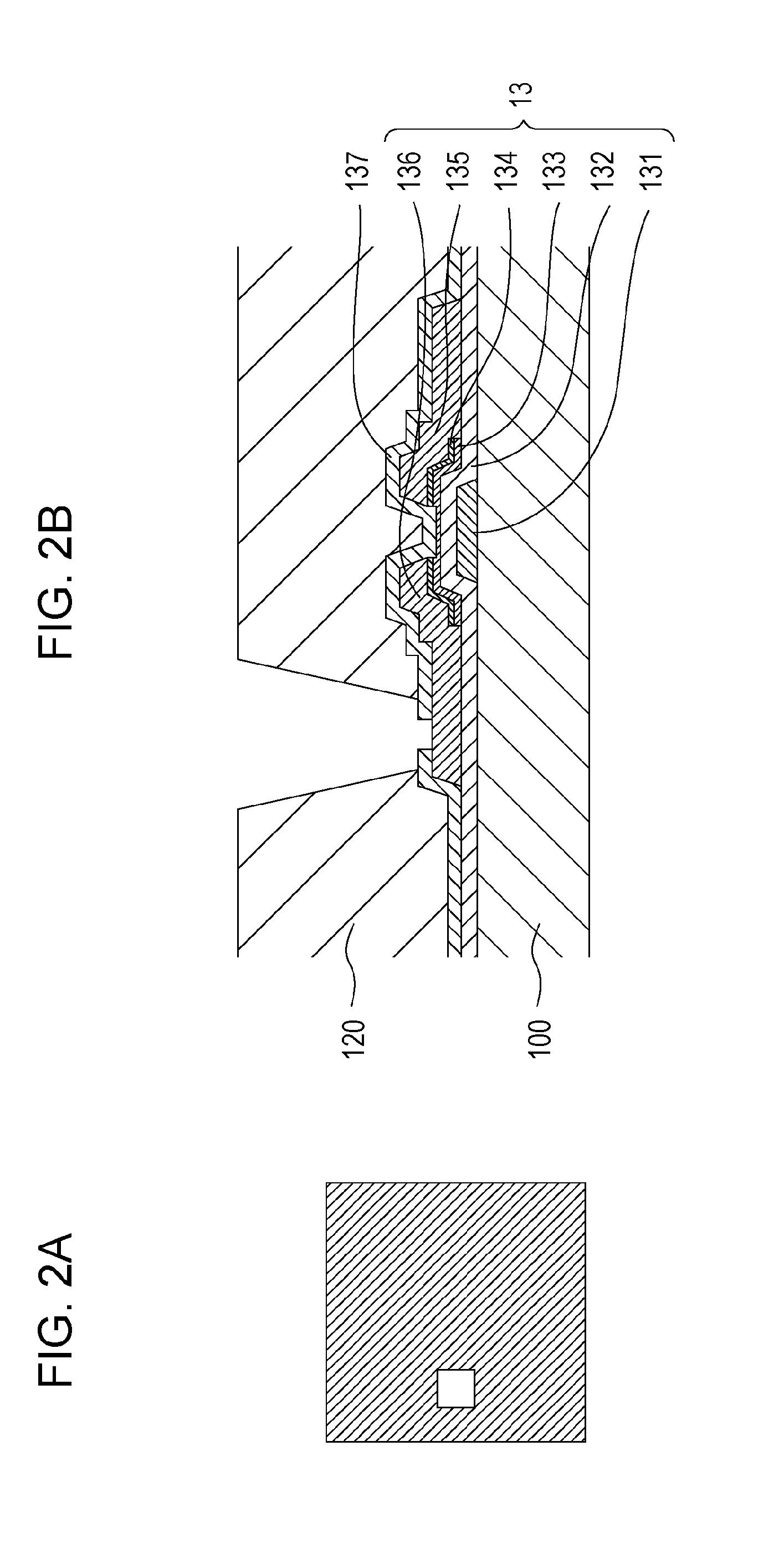
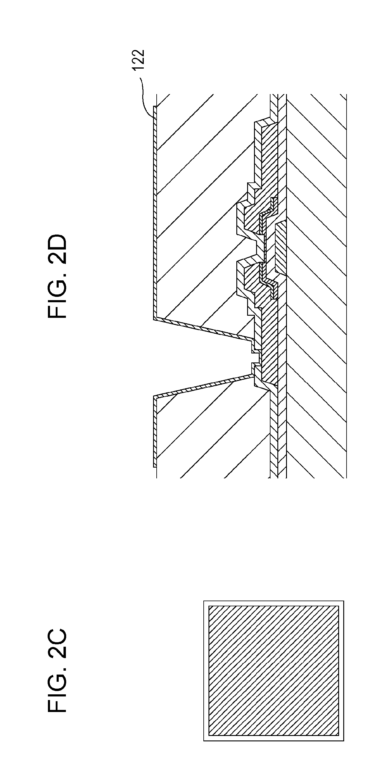
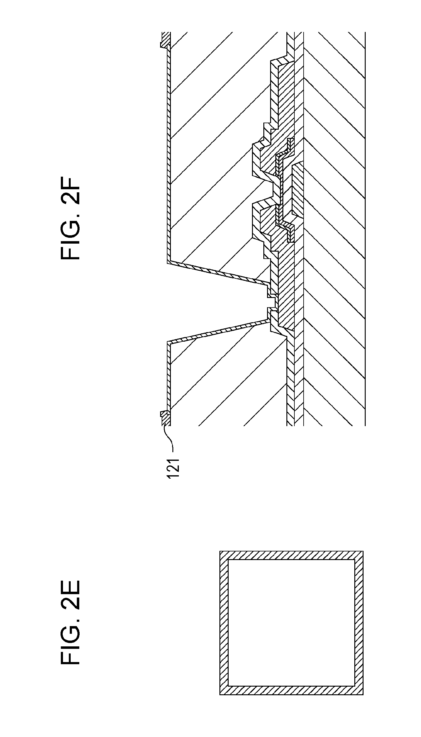
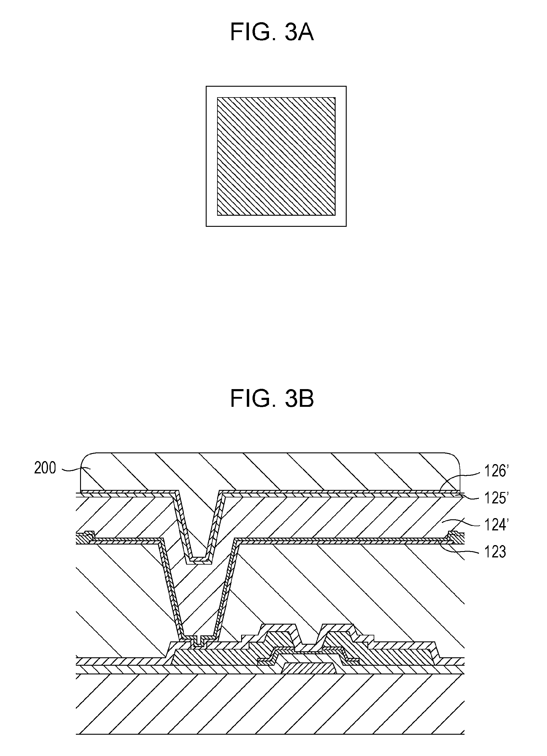
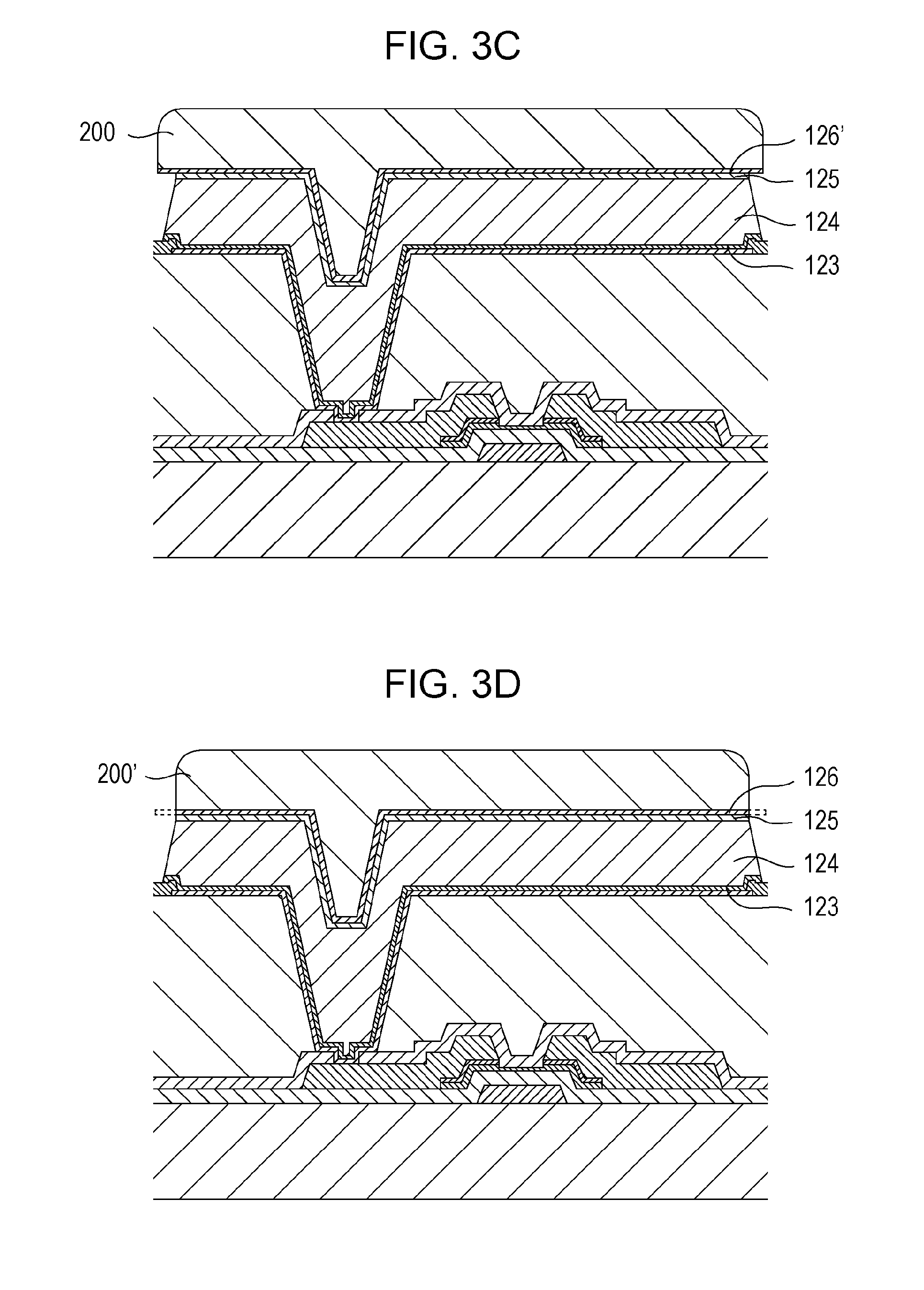
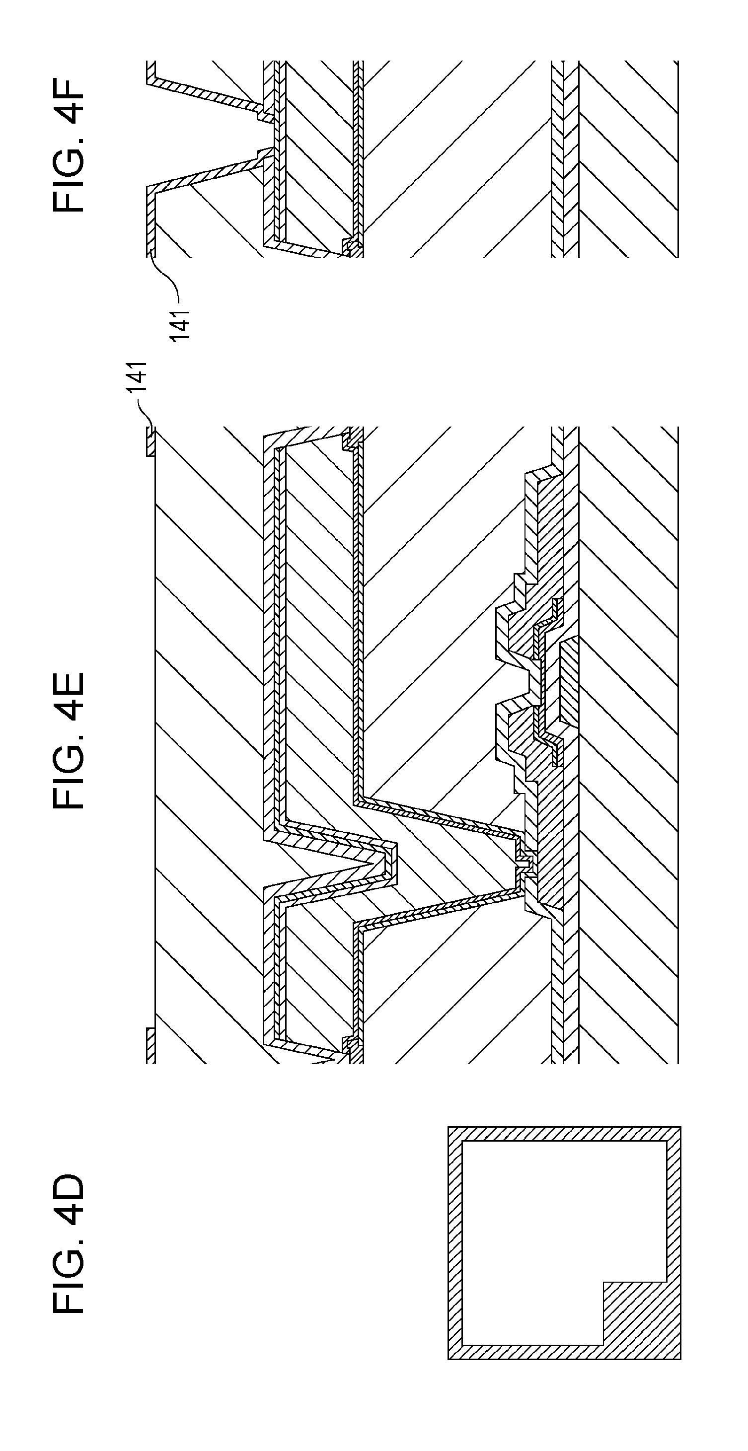
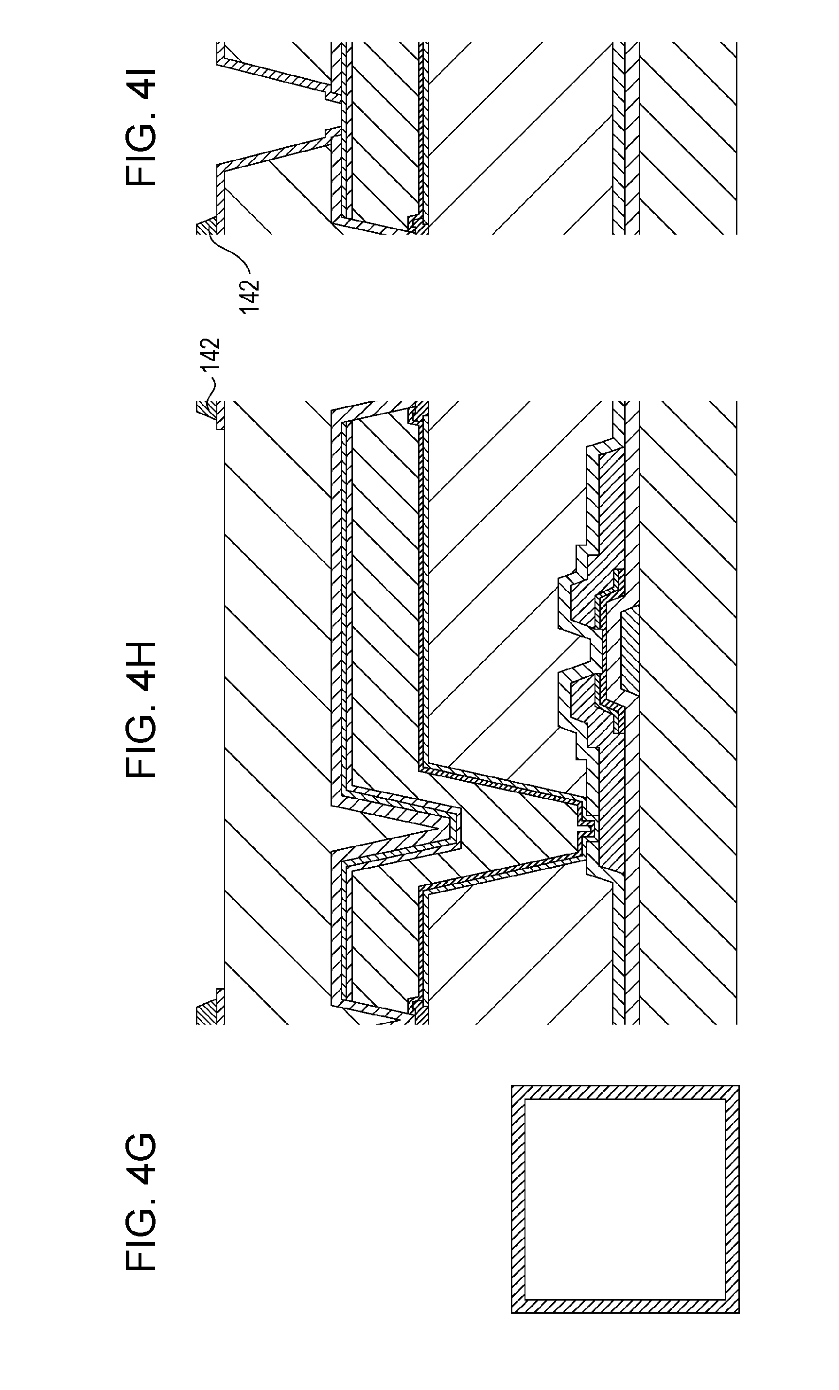
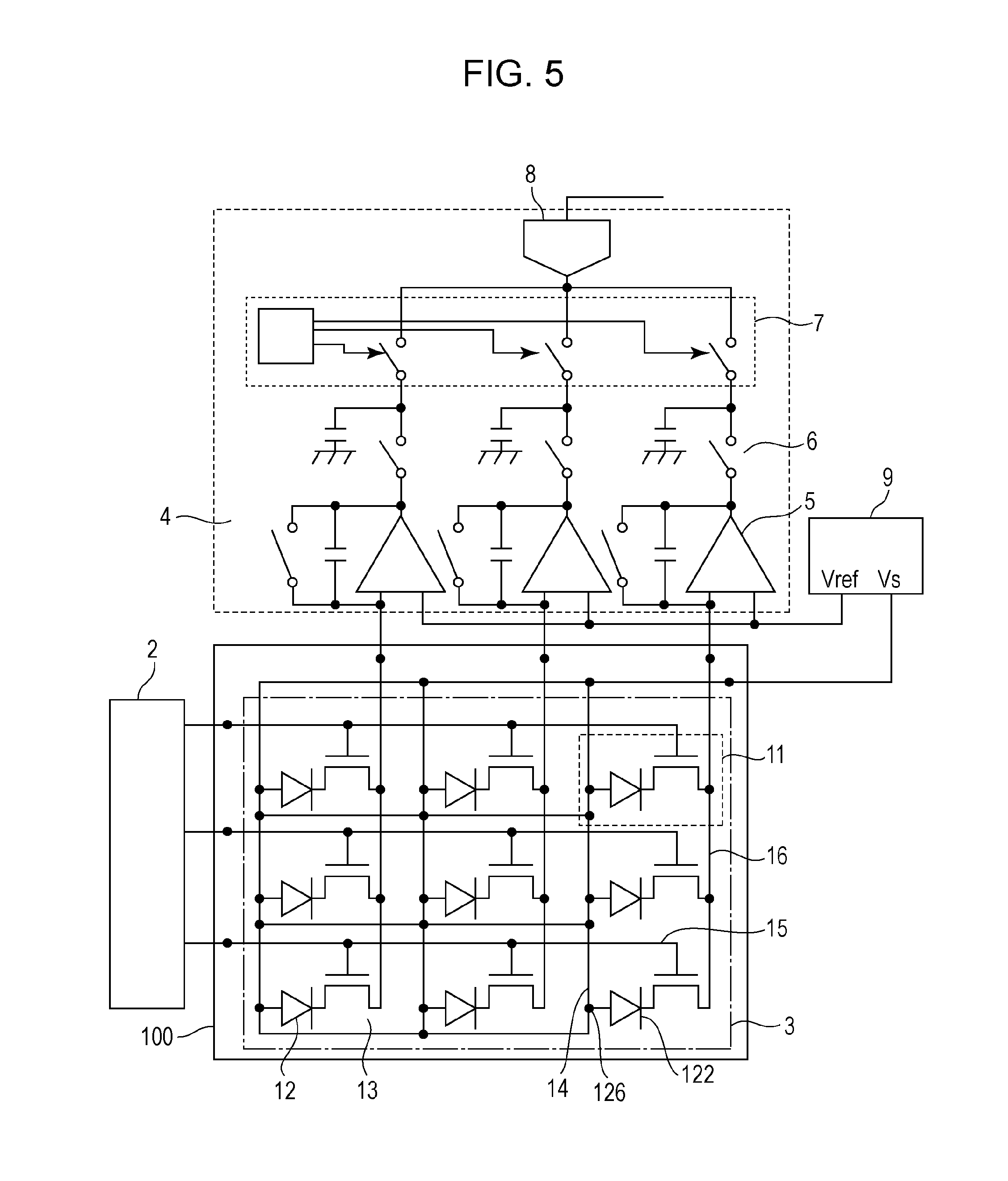
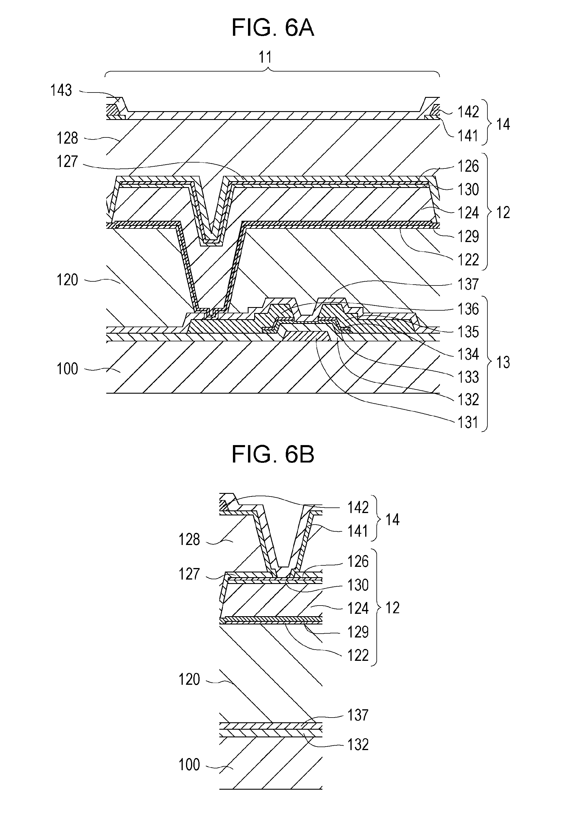
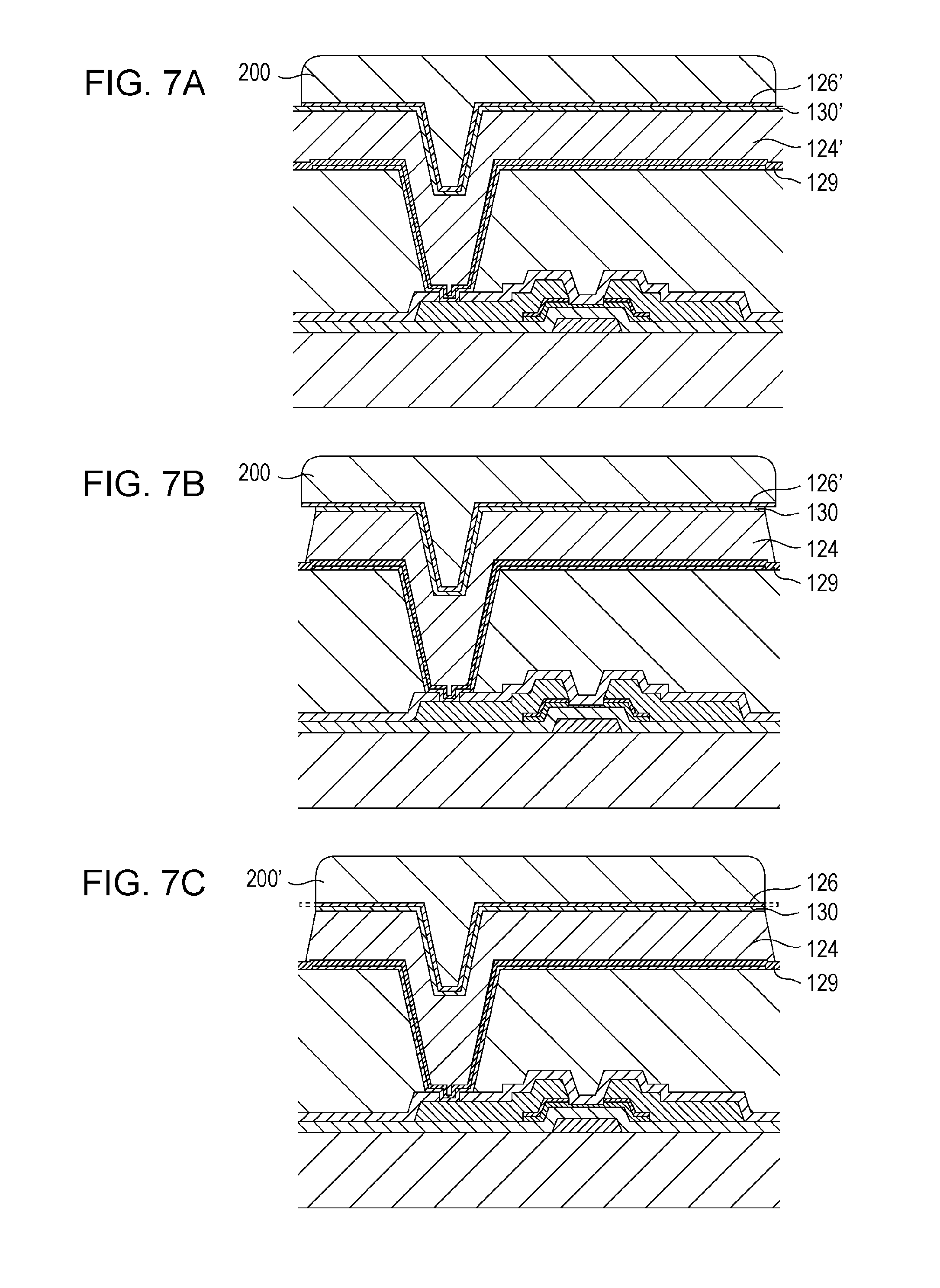
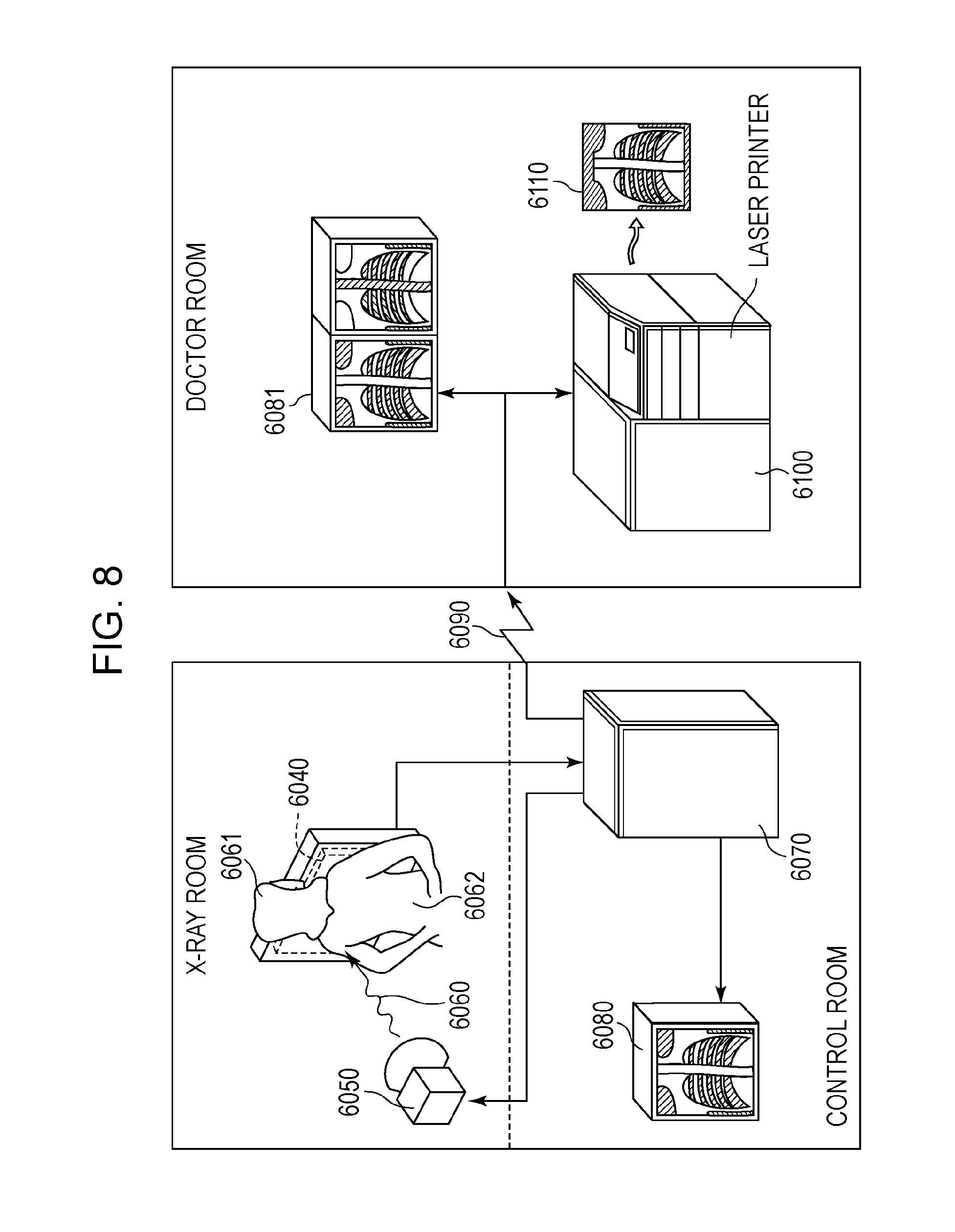
1. Field of the Invention The present application relates to a method of manufacturing a detection device that is applied to, e.g., an image diagnosis apparatus for medical care, a nondestructive inspection apparatus, and an analysis apparatus using radiation. The present application further relates to the detection device and a detection system. 2. Description of the Related Art Recently, the thin-film semiconductor manufacturing technology has been employed to manufacture a detection device including an array of pixels (pixel array), which is a combination of switch elements, e.g., thin-film transistors (TFTs), and conversion elements, e.g., photodiodes, for converting radiation or light to electric charges. Each of pixels in related-art detection devices disclosed in Japanese Patent Laid-Open No. 2004-296654 and No. 2007-059887 includes a conversion element including a first electrode disposed on a substrate, a second electrode disposed above the first electrode, a semiconductor layer disposed between the first electrode and the second electrode, and an the impurity semiconductor layer disposed between the second electrode and the semiconductor layer. The first electrode, the second electrode, the semiconductor layer, and the impurity semiconductor layer are each separated per conversion element, and the second electrode is disposed on the inner side than a region where the impurity semiconductor layer is disposed. In the structure disclosed in Japanese Patent Laid-Open No. 2004-296654 and No. 2007-059887, however, an uncovered region not covered with the second electrode exists in the impurity semiconductor layer, particularly, in the impurity semiconductor layer around the second electrode. Because the impurity semiconductor layer has much higher specific resistance than the second electrode, an electric field tends to be less efficiently applied to a region of the semiconductor layer, which contacts with the uncovered region of the impurity semiconductor layer, in comparison with the case where the second electrode is disposed over the entire impurity semiconductor layer. Even if an electric field is sufficiently applied to the relevant region of the semiconductor layer, when collecting electric charges generated in the relevant region of the semiconductor layer to the second electrode, a distance through which the electric charges generated in the relevant region of the semiconductor layer are moved in the impurity semiconductor layer is longer than a distance through which electric charges generated in a region of the semiconductor layer positioned just under the second electrode are moved. Therefore, a time required to collect the electric charges generated in the above-mentioned relevant region is prolonged and a collection speed of the electric charges is reduced. Thus, there is a possibility that response characteristics, e.g., sensitivity and an operation speed, of the detection device may degrade in comparison with those obtained in the case where the second electrode is disposed over the entire impurity semiconductor layer. With the view of solving the above-described problems in the related art, the present invention provides a detection device that has good response characteristics as a result of suppressing reduction of the response characteristics. According to an embodiment of the present disclosure, there is provided a method of manufacturing a detection device including a plurality of conversion elements disposed on a substrate, each of the conversion elements including a first electrode disposed on the substrate, a second electrode disposed above the first electrode, a semiconductor layer disposed between the first electrode and the second electrode, and an impurity semiconductor layer disposed between the semiconductor layer and the second electrode, the method including a film forming step of successively forming, over the plural first electrodes, a semiconductor film becoming the semiconductor layer, an impurity semiconductor film becoming the impurity semiconductor layer, and an electroconductive film becoming the second electrode in mentioned order, a first removing step of partly removing the electroconductive film, thereby forming an electroconductive layer on each of the plural first electrodes, a second removing step of removing a part of the semiconductor film and a part of the impurity semiconductor film through spaces between the plural electroconductive layers by etching using an etchant having a reaction with the electroconductive film that is slower than a reaction with the impurity semiconductor film and a reaction with the semiconductor film, thereby forming the semiconductor layer and the impurity semiconductor layer on each of the plural first electrodes, and a third removing step of removing a part of the electroconductive layer, the part being positioned on an outer side of the conversion element than an end of the impurity semiconductor layer formed in the second removing step, thereby forming the second electrode. With the embodiment as disclosed herein, the detection device for of suppressing reduction of the response characteristics and having good response characteristics can be provided. Further features of the present invention will become apparent from the following description of exemplary embodiments with reference to the attached drawings. Embodiments of the present invention will be described in detail below with reference to the accompanying drawings. It is to be noted that the term “radiation” used in this specification includes not only beams formed by particles (including photons) emitted through radioactive decay, such as an α-ray, a β-ray, and a γ-ray, but also beams having energy comparable to or more than the above-mentioned beams, such as an X-ray, a corpuscular ray, and a cosmic ray. The structure of one pixel in a detection device according to a first embodiment of the present disclosure is first described with reference to One pixel 11 in the detection device according to the first embodiment of the present disclosure includes a conversion element 12 for converting radiation or light to electric charges, and a TFT (thin-film transistor) 13 serving as a switch element that transfers an electric signal corresponding to the electric charges converted by the conversion element 12. The conversion element 12 may be constituted as an indirect conversion element including a photoelectric conversion element and a wavelength converter for converting radiation to light in a wavelength band sensible by the photoelectric conversion element, or as a direct conversion element for directly converting radiation to electric charges. In this embodiment, a PIN photodiode made of primarily amorphous silicon is used as a photodiode that is one type of photoelectric conversion elements. The conversion element 12 is stacked above the TFT 113, which is disposed on an insulating substrate 100, e.g., a glass substrate, with a passivation layer 137 and a first interlayer insulating layer 120 interposed between the conversion element 12 and the TFT 113. The TFT 13 includes a control electrode 131, a gate insulating layer 132, a semiconductor layer 133, an impurity semiconductor layer 134 having a higher impurity concentration than the semiconductor layer 133, a first main electrode 135, and a second main electrode 136, which are successively formed on the substrate 100 in the mentioned order from the substrate side. The control electrode 131 serves as a gate electrode of the TFT 13. The first main electrode 135 serves as one of a source electrode and a drain electrode of the TFT 13. The second main electrode 136 serves as the other of the source electrode and the drain electrode of the TFT 13. Partial regions of the impurity semiconductor layer 134 are contacted with the first main electrode 135 and the second main electrode 136, respectively. A region of the semiconductor layer 133, which is positioned between regions thereof contacting respectively with the above-mentioned partial regions of the impurity semiconductor layer 134, serves as a channel region of the TFT 13. The control electrode 131 is electrically connected to a control wiring 15. The first main electrode 135 is electrically connected to a signal wiring 16, and the second main electrode 136 is electrically connected to a first electrode 122 of the conversion element 12. In this embodiment, the first main electrode 135 and the signal wiring 16 are integrally constituted by the same electroconductive layer, and the first main electrode 135 is a part of the signal wiring 16. Furthermore, in this embodiment, the control electrode 131 and the control wiring 15 are integrally constituted by the same electroconductive layer, and the control electrode 131 is a part of the control wiring 15. The passivation layer 137 is made of an inorganic insulating material, e.g., silicon oxide or silicon nitride, and is disposed to cover the TFT 13, the control wiring 15, and the signal wiring 16. While, in this embodiment, an inverted-staggered TFT using the semiconductor layer 133 and the impurity semiconductor layer 134, each made of primarily amorphous silicon, is used as the switch element, the switch element used in the present invention is not limited to that type. As another example, a staggered TFT made of primarily polycrystalline silicon, an organic TFT, or an oxide TFT may also be used. The first interlayer insulating layer 120 is disposed between the substrate 100 and the plural first electrodes 122 to cover the plural TFTs 13, and it has contact holes. The first electrode 122 of the conversion element 12 and the second main electrode 136 of the TFT 13 are electrically connected to each other in the contact hole formed in the first interlayer insulating layer 120. The first interlayer insulating layer 120 is advantageously made of an organic insulating material, which can be formed thick, to reduce a parasitic capacity between the conversion element 12 and each of the TFT 13, the control wiring 15, and the signal wiring 16. The conversion element 12 includes the first electrode 122, an impurity semiconductor layer 123 of first conductivity type, a semiconductor layer 124, an impurity semiconductor layer 125 of second conductivity type, and the second electrode 126, which are successively formed on the first interlayer insulating layer 120 in the mentioned order from the first interlayer insulating layer side. Herein, the semiconductor layer 124 disposed between the first electrode 122 and the second electrode 126 is desirably an intrinsic semiconductor. The impurity semiconductor layer 123 of first conductivity type disposed between the first electrode 122 and the semiconductor layer 124 exhibits a polarity of first conductivity type, and it contains impurities of first conductivity type at a higher concentration than the semiconductor layer 124 and the impurity semiconductor layer 125 of second conductivity type. The impurity semiconductor layer 125 of second conductivity type disposed between the semiconductor layer 124 and the second electrode 126 exhibits a polarity of second conductivity type opposite to the first conductivity type, and it contains impurities of second conductivity type at a higher concentration than the impurity semiconductor layer 123 of first conductivity type and the semiconductor layer 124. The first conductivity type and the second conductivity type are conductivity types differing in polarity from each other. For example, when the first conductivity type is n-type, the second conductivity type is p-type. An electrode wiring 14 (described later) is electrically connected to the second electrode 126 of the conversion element 12. The first electrode 122 of the conversion element 12 is electrically connected to the second main electrode 136 of the TFT 13 in the contact hole formed in the first interlayer insulating layer 120. While this embodiment employs the photodiode including the impurity semiconductor layer 123 of first conductivity type, the semiconductor layer 124, and the impurity semiconductor layer 125 of second conductivity type, those layers being made of primarily amorphous silicon, the photodiode usable in the present application is not limited to that type. As another example, an element of directly converting radiation to electric charges may also be used. Such an element may include the impurity semiconductor layer 123 of first conductivity type, the semiconductor layer 124, and the impurity semiconductor layer 125 of second conductivity type, those layers being made of primarily amorphous selenium. The first electrode 122 and the second electrode 126 of the conversion element 12 are each made of a transparent electroconductive oxide, e.g., light-transmissive ITO. However, the first electrode 122 may be made of a metallic material. In particular, when the conversion element 12 is an indirect conversion element including a photoelectric conversion element and a wavelength converter, the transparent electroconductive oxide, e.g., light-transmissive ITO, is used for the second electrode 126 that is an electrode positioned on the wavelength converter side. On the other hand, the first electrode 122 positioned farther away from the wavelength converter than the second electrode 126 may be made of an electrical conductor made of Al and having low light transmissivity. In this embodiment of the present disclosure, the impurity semiconductor layer 125 of second conductivity type and the second electrode 126 are disposed such that an end of the impurity semiconductor layer 125 of second conductivity type and an end of the second electrode 126 are positioned on a linear line in a direction perpendicular to their surfaces. Between adjacent two of the plural first electrodes 122 on the first interlayer insulating layer 120, an insulating member (layer) 121 made of an inorganic insulating material is disposed in contact with the first interlayer insulating layer 120. Thus, the first electrode 122 and the insulating member 121 are disposed on the first interlayer insulating layer 120 to cover the first interlayer insulating layer 120. Accordingly, when an impurity semiconductor film becoming the impurity semiconductor layer 123 is formed, the surface of the first interlayer insulating layer 120 is not exposed and mixing of an organic insulating material into the impurity semiconductor layer 123 can be reduced. Moreover, in this embodiment, the impurity semiconductor layer 123, the semiconductor layer 124, and the impurity semiconductor layer 125 are separated for each pixel above the insulating member 121. In a dry etching step for that separation, since the insulating member 121 serves as an etching stop layer, the first interlayer insulating layer 120 is avoided from being exposed to species used in the dry etching, and the surrounding layers can be prevented from being contaminated by the organic insulating material. The passivation layer 127 and a second interlayer insulating layer 128 are disposed to cover the conversion element 12. The passivation layer 127 is made of an inorganic insulating material, e.g., silicon oxide or silicon nitride, and it covers the conversion element 12 and the insulating member 121. The second interlayer insulating layer 128 is disposed between the second electrode 126 and the electrode wiring 14 to cover the passivation layer 127. The passivation layer 127 and the second interlayer insulating layer 128 have contact holes. The second electrode 126 of the conversion element 12 and the electrode wiring 14 are electrically connected to each other in the contact holes formed in the passivation layer 127 and the second interlayer insulating layer 128. The second interlayer insulating layer 128 is advantageously made of an organic insulating material, which can be formed thick, to reduce a parasitic capacity between the conversion element 12 and the electrode wiring 14. The electrode wiring 14 includes a first electroconductive layer 141 made of a transparent electroconductive oxide and disposed on the second interlayer insulating layer 128, and a second electroconductive layer 142 made of a metallic material and disposed on the first electroconductive layer 141. The first electroconductive layer 141 is connected to the second electrode 126 of the conversion element 12 in the contact holes formed in the passivation layer 127 and the second interlayer insulating layer 128. The second electroconductive layer 142 is disposed on the first electroconductive layer 141 such that an orthographic projection of the second electroconductive layer 142 is positioned between the two first electrodes 122 of the two conversion elements 12 adjacent to each other. A passivation layer 143 made of an inorganic insulating material, e.g., silicon oxide or silicon nitride, is disposed to cover the electrode wiring 14. A method of manufacturing the detection device according to the first embodiment of the present disclosure will be described below with reference to The plural TFTs 13 are disposed on the insulating substrate 100, and a protective layer 137 is disposed to cover the plural TFTs 13. A contact hole is formed by etching in the protective layer 137 in its portion on the second main electrode 136 where the second main electrode 136 is electrically connected to the photodiode. In a step illustrated in In a step illustrated in In a step illustrated in In a step illustrated in A resist 200 is formed on the transparent electroconductive oxide film with the use of the mask illustrated in In a step illustrated in In view of the above-mentioned problem, in a step illustrated in In consideration of a process margin, however, it is not easy to align the end of the impurity semiconductor layer 125 and the end of the second electrode 126 with each other, and both the ends may slightly shift in some cases. In such a case, the end of the second electrode 126 formed by the third removing step is more advantageously positioned on the inner side of the conversion element 12 relative to the end of the impurity semiconductor layer 125 than being positioned on the outer side thereof. Additionally, a mutual shift between both the ends is allowed when the following formula is satisfied; where a distance between the end of the second electrode 126 and the end of the impurity semiconductor layer 125 is D (μm), a width of the conversion element 12 is P (μm), sheet resistance of the impurity semiconductor layer 125 is Rs (Ω), and on-resistance of the TFT 13 is Ron (Ω). While this embodiment has been described in connection with the method of etching the electroconductive film, the impurity semiconductor layer 125, etc. without removing the resist 200, the present disclosure is not limited to that method. An alternative method is, for example, as follows. The resist 200 is removed after the step illustrated in In a step illustrated in In a step illustrated in In a step illustrated in An equivalent circuit of the detection device according to the first embodiment of the present application will be described below with reference to The operation of the detection device according to this embodiment will be described below. The reference potential Vref is applied to the first electrode 122 of the conversion element 12 through the TFT 13, and the bias potential Vs necessary for separating an electron-hole pair, generated by radiation or visible light, is applied to the second electrode 126. In such a state, the radiation having transmitted through a subject or the visible light corresponding to that radiation enters the conversion element 12 and is converted to electric charges, which are accumulated in the conversion element 12. An electric signal corresponding to the electric charges are output to the signal wiring 16 upon the TFF 13 being brought into a conducted state with a drive pulse applied to the control wiring 15 from the drive circuit 2. The electric signal is then read out as digital data to the exterior by the read circuit 4. The structure of one pixel in a detection device according to a second embodiment of the present disclosure will be described below with reference to In the second embodiment, an MIS photoelectric conversion element is used as the conversion element 12 instead of the PIN photodiode used in the first embodiment. In more detail, the conversion element 12 includes a first electrode 122, an insulating layer 129, a semiconductor layer 124, an impurity semiconductor layer 130 of first conductivity type, and a second electrode 126, which are successively formed on the first interlayer insulating layer 120 in the mentioned order from the first interlayer insulating layer side. Herein, the insulating layer 129 disposed between the first electrode 122 and the semiconductor layer 124 is not separated per the conversion element 12 and is disposed to extend over the plural conversion elements 12. Therefore, the insulating member 121 in the first embodiment is not used in the second embodiment. A method of manufacturing the detection device according to the second embodiment will be described below with reference to In a step illustrated in In a step illustrated in At that time, the insulating layer 129 is not entirely removed, and a part of the insulating layer 129 remains as it is. As a result, the semiconductor layer 124, the impurity semiconductor layer 130, and the electroconductive layer 126′ are formed on each of the plural first electrodes 122. Herein, the impurity semiconductor layer 130 is obtained by partly removing the impurity semiconductor film 130′. Such a step also corresponds to the second removing step. The above-described pixel separation by the dry etching is effectuated on the insulating layer 129. Accordingly, the insulating layer 129 functions as an etching stop layer, whereby the first interlayer insulating layer 120 is avoided from being exposed to species used in the dry etching and the surrounding layers can be prevented from being contaminated by the organic insulating material. A similar etchant to that used in the first embodiment is also used for the dry etching in the second embodiment. With the dry etching, as described above, the respective ends of the impurity semiconductor layer 130 and the semiconductor layer 124 are retracted from the end of the resist 200 such that the end of the impurity semiconductor layer 130 is positioned on the inner side than the end of the electroconductive layer 126′. In a step illustrated in A radiation detection system using the detection device according to the embodiment of the present application will be described below with reference to An X-ray 6060 emitted from an X-ray tube 6050, i.e., a radiation source, transmits through the chest 6062 of a patient or a subject 6061 and enters individual conversion elements 12 of the conversion section 3 included in a radiation detection device 6040. The X-ray having entered the conversion elements 12 contains information regarding the interior of a body of the patient 6061. Upon the incidence of the X-ray, the radiation is converted to electric charges and electrical information is obtained in the conversion section 3. The obtained electrical information is converted to digital data and is subjected to image processing in an image processor 6070, i.e., an image processing unit, such that the information can be observed on a display 6080, i.e., a display unit, in a control room. Furthermore, the obtained information can be transferred to a remote place via a transmission processing unit, such as a telephone line 6090, and can be displayed on a display 6081, i.e., a display unit, or stored in a storage unit, e.g., an optical disk, in a doctor room at a different location. This enables a doctor at the remote place to make a diagnosis. As an alternative, the obtained information can be recorded on a film 6110, i.e., a recording medium, by a film processor 6100, i.e., a recording unit. While the present invention has been described with reference to exemplary embodiments, it is to be understood that the invention is not limited to the disclosed exemplary embodiments. The scope of the following claims is to be accorded the broadest interpretation so as to encompass all such modifications and equivalent structures and functions. This application claims the benefit of Japanese Patent Application No. 2012-106883 filed May 8, 2012, which is hereby incorporated by reference herein in its entirety. Before transmitting a print job to a printing apparatus, a CPU of a print processing apparatus determines whether paper information designated in the print job has been registered in a paper information database of the print processing apparatus. If the paper information has not been registered, the CPU extracts paper information similar to the paper information designated in the print job from those stored in the paper information database of the print processing apparatus. Furthermore, the CPU copies information about the dependency on the printing apparatus, which is included in the extracted paper information (printer dependency information) to the paper information designated in the print job. Then, the CPU registers the paper information designated in the print job, to which the printer dependency information has been copied, in a paper information database of the printing apparatus and transmits the print job to the printing apparatus. 1. A method of manufacturing a detection device that includes a plurality of conversion elements disposed on a substrate, each of the conversion elements comprising a first electrode disposed on the substrate, a second electrode disposed above the first electrode, a semiconductor layer disposed between the first electrode and the second electrode, and an impurity semiconductor layer disposed between the semiconductor layer and the second electrode, the method comprising:
a film forming step of successively forming, over the plural first electrodes, a semiconductor film becoming the semiconductor layer, an impurity semiconductor film becoming the impurity semiconductor layer, and an electroconductive film becoming the second electrode, in mentioned order; a first removing step of partly removing the electroconductive film with use of a resist formed on the electroconductive film, thereby forming an electroconductive layer on each of the plural first electrodes; a second removing step of removing, with use of the resist, a part of the semiconductor film and a part of the impurity semiconductor film through spaces between the plural electroconductive layers by etching using an etchant having a reaction with the electroconductive film that is slower than a reaction with the impurity semiconductor film and a reaction with the semiconductor film, thereby forming the semiconductor layer and the impurity semiconductor layer on each of the plural first electrodes; and a third removing step of removing a part of the electroconductive layer, the part being positioned on an outer side of the conversion element than an end of the impurity semiconductor layer formed in the second removing step, with use of an adjusted resist, which is obtained by removing a part of the aforesaid resist such that an end of the aforesaid resist and the end of the impurity semiconductor layer are positioned on a linear line, thereby forming the second electrode. 2. The method of manufacturing the detection device according to 3. The method of manufacturing the detection device according to 4. The method of manufacturing the detection device according to the method further comprises the steps of: forming a contact hole in an interlayer insulating film formed to cover the thin-film transistors, which are disposed on the substrate, at a position above each of the thin-film transistors, thereby forming a first interlayer insulating layer; and partly removing an electroconductive film formed to cover the thin-film transistors and the first interlayer insulating layer, thereby forming the plural first electrodes. 5. The method of manufacturing the detection device according to the method further comprises, between the first electrode forming step and the film forming step, a step of partly removing an insulating film made of an inorganic insulating material, which is formed to cover the first interlayer insulating layer made of an organic insulating material and the first electrodes, thereby forming an insulating member such that a surface of the first interlayer insulating layer is covered with the insulating member and the first electrode, and the second removing step is performed above the insulating member. 6. The method of manufacturing the detection device according to in the film forming step, the insulating layer, the semiconductor film becoming the semiconductor layer, the impurity semiconductor film becoming the impurity semiconductor layer, and the electroconductive film becoming the second electrode are successively formed over the plural first electrodes, in mentioned order, and in the second removing step, the semiconductor layer, the impurity semiconductor layer, and the electroconductive layer are formed on each of the plural first electrodes by removing a part of the electroconductive film, a part of the impurity semiconductor layer, and a part of the semiconductor film, while the insulating layer is left to remain. 7. The method of manufacturing the detection device according to 8. The method of manufacturing the detection device according to forming a contact hole in an interlayer insulating film formed to cover the conversion element at a position above the second electrode, thereby forming a second interlayer insulating layer; partly removing a transparent electroconductive oxide film formed to cover the second interlayer insulating layer and the second electrode, thereby forming a first electroconductive layer; and partly removing a metal film formed to cover the first electroconductive layer and the second interlayer insulating layer, thereby forming a second electroconductive layer on the first electroconductive layer, the second electroconductive layer being formed such that an orthographic projection of the second electroconductive layer is positioned between the two first electrodes adjacent to each other. 9. A detection device manufactured by the manufacturing method according to 10. A detection system comprising:
the detection device according to a signal processing unit configured to process a signal from the detection device; a display unit configured to display the signal from the signal processing unit; and a transmission processing unit configured to transmit the signal from the signal processing unit.BACKGROUND OF THE INVENTION
SUMMARY OF THE INVENTION
BRIEF DESCRIPTION OF THE DRAWINGS
DESCRIPTION OF THE EMBODIMENTS
First Embodiment
4×Second Embodiment
Application Embodiment
4×