STACKED PACKAGE OF VOLTAGE REGULATOR AND METHOD FOR FABRICATING THE SAME
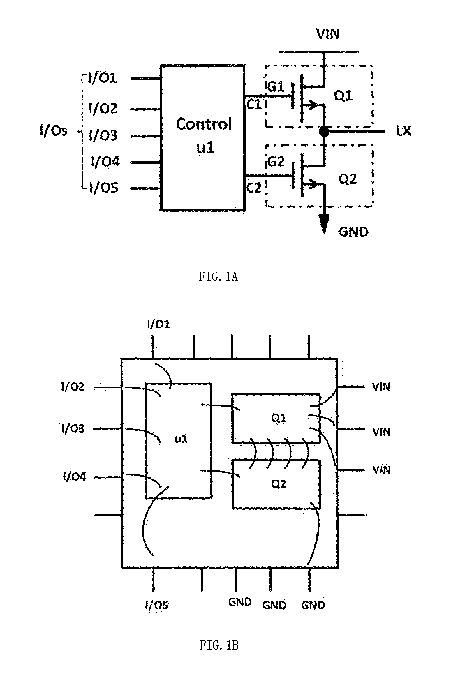
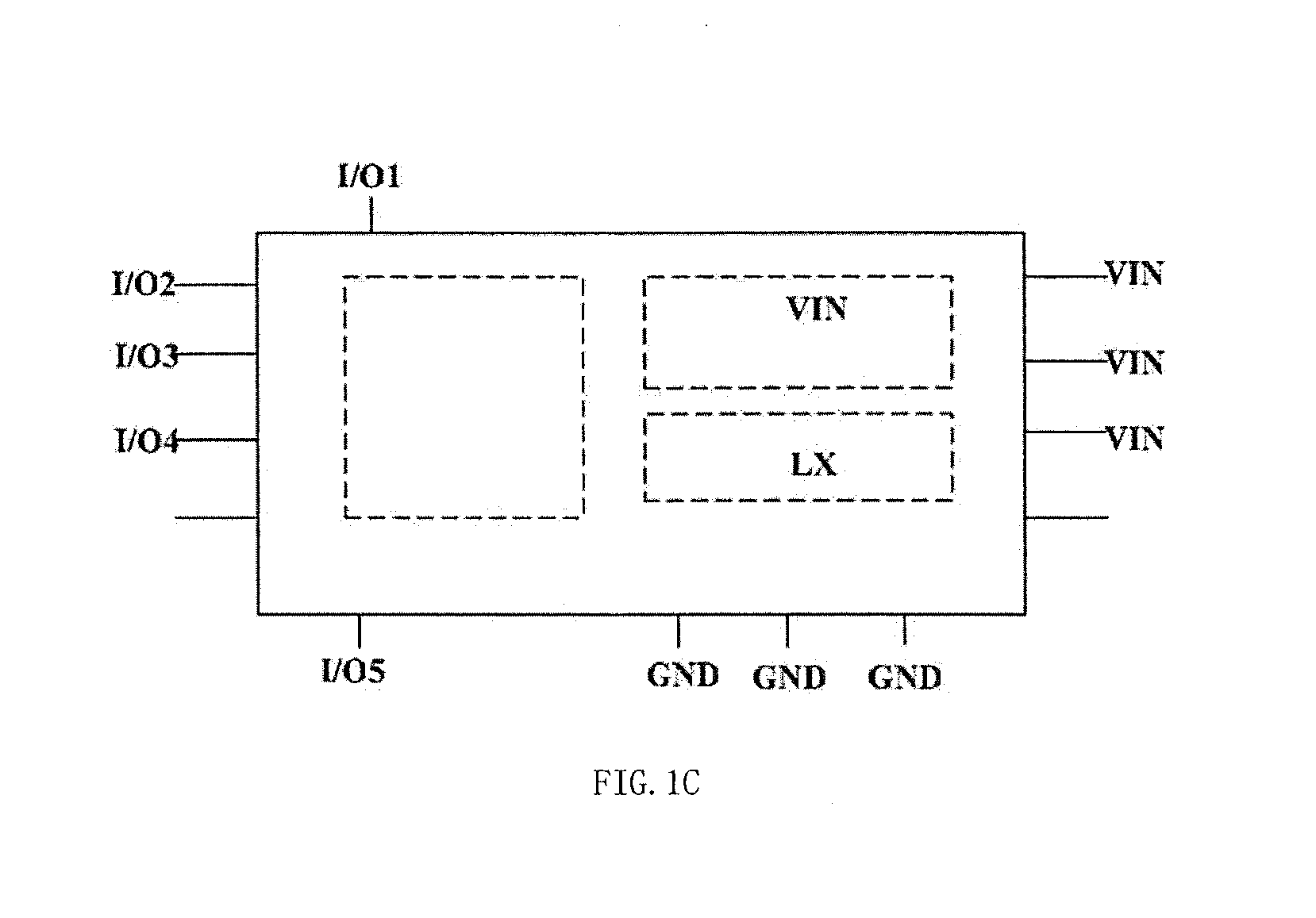
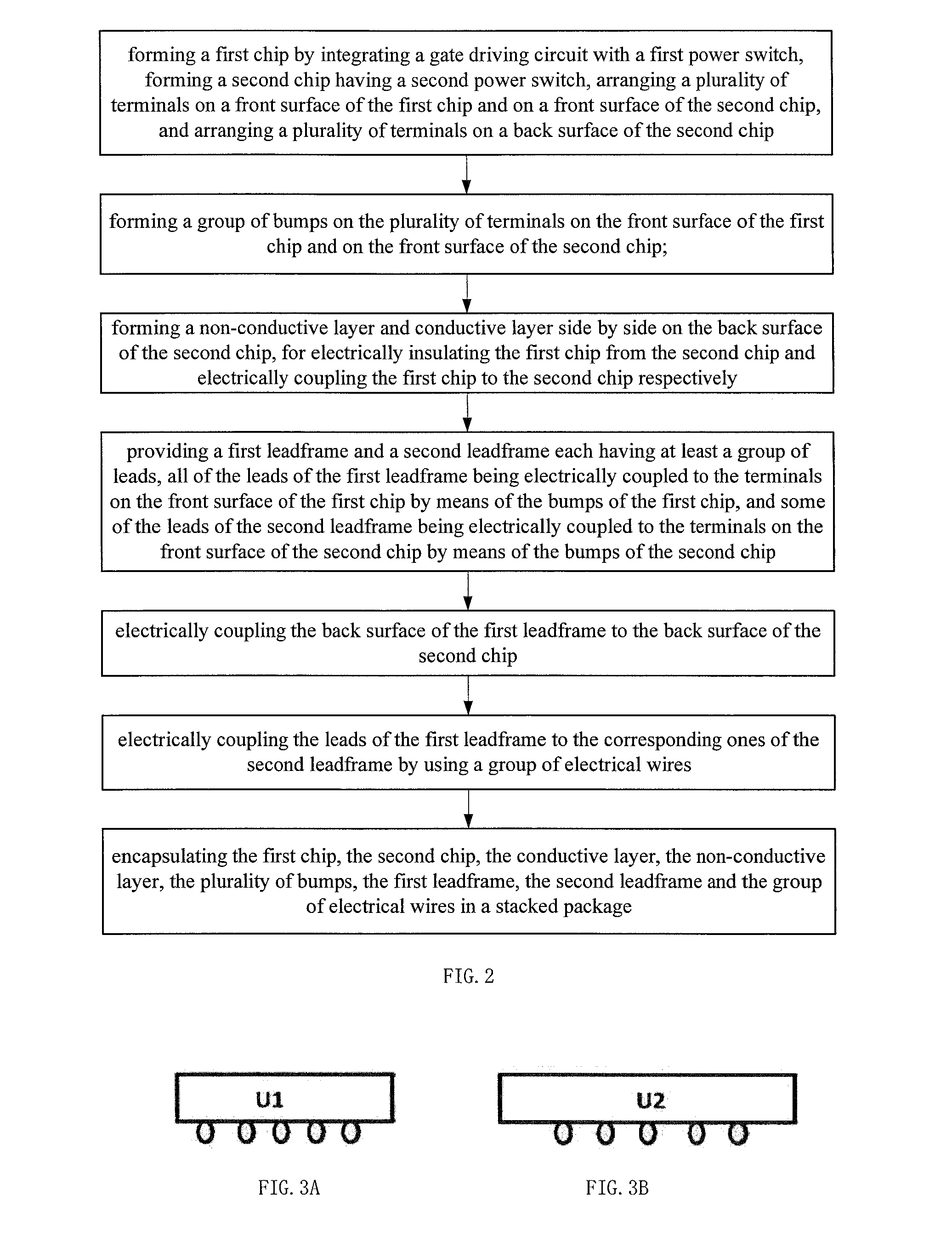
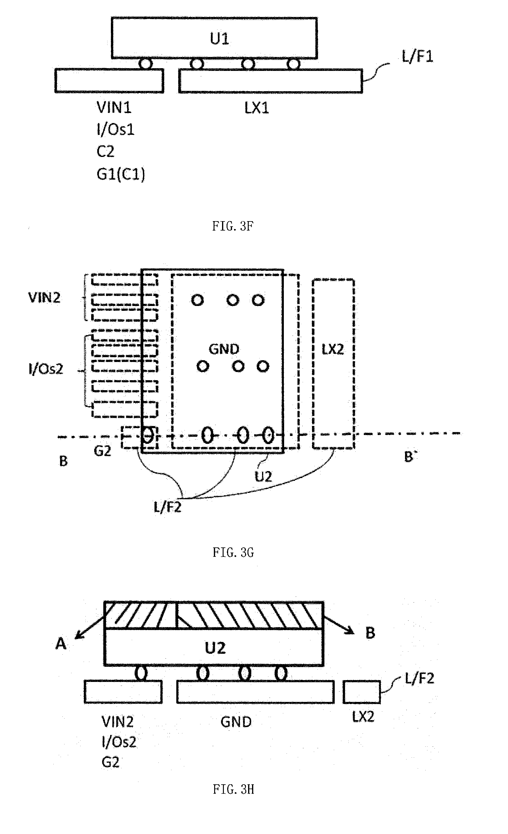
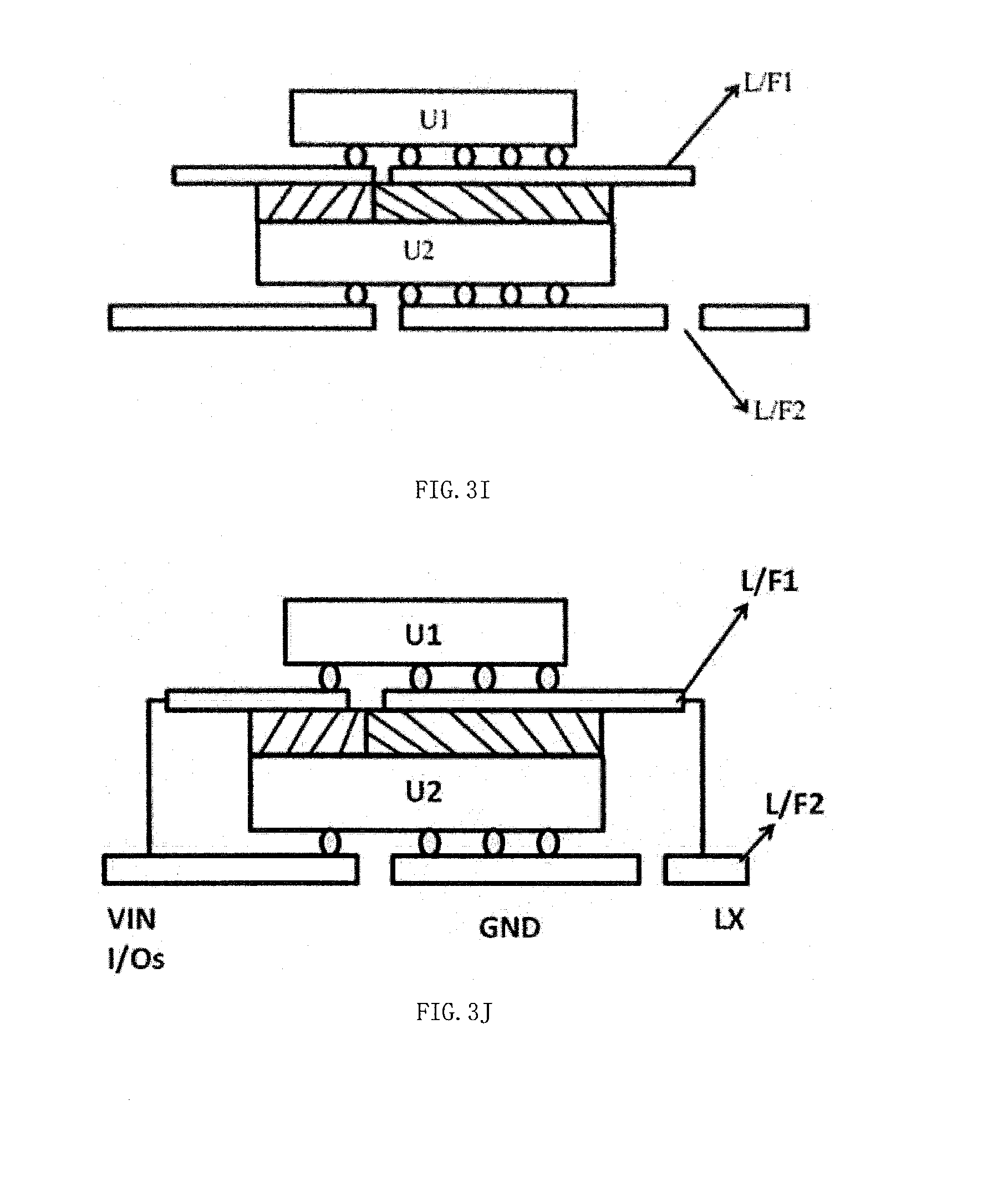
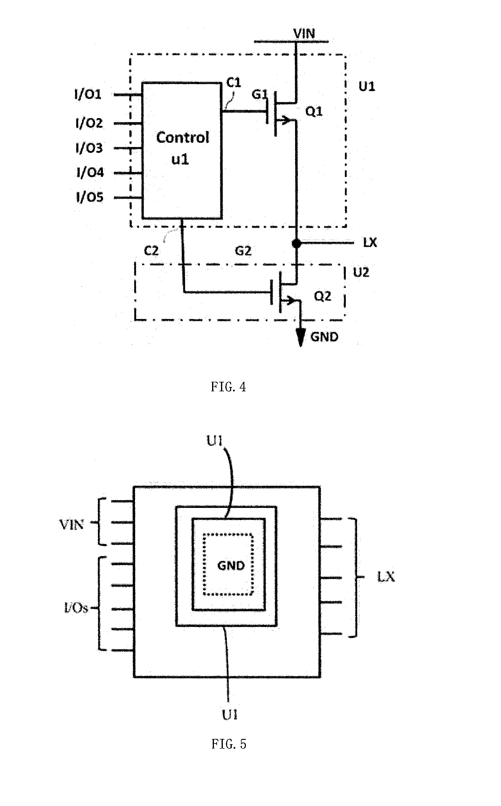
This application claims the benefit of Chinese Patent Application No. 201310378482.X, filed on Aug. 27, 2013, which is incorporated herein by reference in its entirety. The present disclosure generally relates to the field of semiconductor chip package, and more specifically, to a stacked package of a voltage regulator and a method for fabricating the same. As the demand for miniaturization, low manufacture cost, high density and multi-functionality of electronic products, chip packages continue to advance towards the package technology that a plurality of dies are encapsulated in one encapsulant. An example of a switching voltage regulator will now be described to show some features of the prior package technology, with reference to An important concern in the chip package technology is a ratio of a chip footprint to a package area. The package technology is advantageous if the ratio has a value of approximately 1. However, the above chip package structure means that the chip package has an area at least larger than a sum of the three independent chips. Consequently, it has a large package area and results in a high manufacture cost. One object of the present disclosure is to provide a stacked package of a voltage regulator and a method for fabricating the same. To solve the above problem, there is provided a method for fabricating a stacked package of a voltage regulator, comprising: forming a first chip by integrating a gate driving circuit with a first power switch, forming a second chip having a second power switch, arranging a plurality of terminals on a front surface of the first chip and on a front surface of the second chip, and arranging a plurality of terminals on a back surface of the second chip; forming a group of bumps corresponding to the plurality of terminals on the front surface of the first chip and on the front surface of the second chip; forming a non-conductive layer and conductive layer side by side on the back surface of the second chip, for electrically insulating the first chip from the second chip and electrically coupling the first chip to the second chip respectively; providing a first leadframe and a second leadframe each having at least a group of leads, all of the leads of the first leadframe being electrically coupled to the terminals on the front surface of the first chip by means of the bumps of the first chip, and some of the leads of the second leadframe being electrically coupled to the terminals on the front surface of the second chip by means of the bumps of the second chip; electrically coupling the back surface of the first leadframe to the back surface of the second chip; electrically coupling the leads of the first leadframe to the corresponding ones of the second leadframe by using a group of electrical wires so that the leads of the second leadframe may be coupled to an external circuit; and encapsulating the first chip, the second chip, the conductive layer, the non-conductive layer, the plurality of bumps, the first leadframe, the second leadframe and the group of electrical wires in a stacked package. Preferably, the method further comprises: attaching a printed circuit to the back surface of the second leadframe. Preferably, the leads are finger-like or block-like. Preferably, the conductive layer has a thickness the same as that of the non-conductive layer. Preferably, the conductive layer has an area larger than that of the non-conductive layer. Preferably, the electrical wires are copper clips. Preferably, the bumps are one selected from the group consisting of copper posts, solder bumps, and composite bumps formed by electroless nickel immersion gold. Preferably, the voltage regulator is a switching voltage regulator. Another object is to provide a stacked package comprising: a first chip having a gate driving circuit and a first power switch which are integrated with each other, the first chip having a front surface with a plurality of terminals thereon; a second chip having a second power switch, the second chip having a front surface and a back surface with a plurality of terminals thereon; a non-conductive layer and conductive layer side by side on the back surface of the second chip, for electrically insulating the first chip from the second chip and electrically coupling the first chip to the second chip respectively; a first leadframe and a second leadframe each having at least a group of leads, the back surface of the first leadframe being electrically coupled to the back surface of the second chip; a group of bumps corresponding to the terminals on the front surface of the first chip and on the front surface of the second chip respectively, for electrically coupling the terminals on the front surface of the first chip to the leads of the first leadframe and electrically coupling the terminals on the front surface of the second chip to some of the leads of the second leadframe respectively; a group of electrical wires for electrically coupling the leads of the first leadframe to the leads of the second leadframe; and an encapsulant for encapsulating the first chip, the second chip, the conductive layer, the non-conductive layer, the plurality of bumps, the first leadframe, the second leadframe and the group of electrical wires. Preferably, the voltage regulator further comprises: a printed circuit attaching to the back surface of the second leadframe. Preferably, the leads are finger-like or block-like. Preferably, the conductive layer has a thickness the same as that of the non-conductive layer. Preferably, the conductive layer has an area larger than that of the non-conductive layer. Preferably, the electrical wires are copper clips. Preferably, the bumps are one selected from the group consisting of copper posts, solder bumps, and composite bumps formed by electroless nickel immersion gold. In view of that above technical solutions, the present disclosure relates to a method for fabricating a stacked package of a voltage regulator, comprises: forming a first chip by integrating a gate driving circuit with a first power switch, forming a second chip having a second power switch, arranging a plurality of terminals on a front surface of the first chip and on a front surface of the second chip, and arranging a plurality of terminals on a back surface of the second chip; forming a group of bumps corresponding to the plurality of terminals on the front surface of the first chip and on the front surface of the second chip; forming a non-conductive layer and conductive layer side by side on the back surface of the second chip, for electrically insulating the first chip from the second chip and electrically coupling the first chip to the second chip respectively; providing a first leadframe and a second leadframe each having at least a group of leads, all of the leads of the first leadframe being electrically coupled to the terminals on the front surface of the first chip by means of the bumps of the first chip, and some of the leads of the second leadframe being electrically coupled to the terminals on the front surface of the second chip by means of the bumps of the second chip; electrically coupling the back surface of the first leadframe to the back surface of the second chip; electrically coupling the leads of the first leadframe to the corresponding ones of the second leadframe by using a group of electrical wires; and encapsulating the first chip, the second chip, the conductive layer, the non-conductive layer, the plurality of bumps, the first leadframe, the second leadframe and the group of electrical wires in a stacked package. In the present method for fabricating the stacked package, the conductive layer and the non-conductive layer are used for electrically insulating and coupling different parts of the integrated circuit. The stacked package of the voltage regulator is obtained by stacking the first chip on the second chip by using the first leadframe and the second leadframe. Thus, the stacked package formed by the present method has a small size, a high integration density and improved performance. Moreover, no bonding wires are used in the chip package where the first chip is stacked on the second chip by using a first leadframe and a second leadframe, which results in less power loss and higher efficiency. Objects, features and advantages of the present disclosure will become apparent from the following detailed description of particular embodiments of the present disclosure, with reference to the accompanying drawings. Some particular details will be described for thorough understanding of the present disclosure. However, the present disclosure may be practiced with or without these particular details by one skilled person, without departing the principles of the present disclosure. Thus, the present disclosure is not limited to the particular embodiments below. As an example, a method for fabricating a stacked package of a voltage regulator according to the present disclosure will be described with reference to the flow chart shown in Firstly, a first chip U1 is formed by integrating a gate driving circuit u1 with a power switch Q1, as shown in Alternatively, a first chip U1 is formed by integrating a gate driving circuit u1 with a power switch Q2, as shown in Only the previous arrangement will be described in the following steps, as an example of the method for fabricating the stacked package of the voltage regulator according to the present disclosure. However, it will be understood by one skilled person that the other arrangement may also be used in the method for fabricating the stacked package of the voltage regulator according to the present disclosure. In the present embodiment, the two power switches Q1 and Q2 are metal-oxide-semiconductor field effect transistors (MOSFETs). It should be understood that the two power switches may be any semiconductor switches in the art. Specifically, the gate driving circuit u1 has input/output terminal I/Os and driving output terminals C1 and C2, as shown in Preferably, the bumps are one selected from the group consisting of copper posts, solder bumps, and composite bumps formed by electroless nickel immersion gold. Next, a non-conductive layer A and a conductive layer B are formed in two different areas on the back surface of the second chip, for electrically insulating the first chip U1 from the second chip U2 and electrically coupling the first chip U1 to the second chip U2 respectively. Preferably, the conductive layer has a thickness the same as that of the non-conducting layer so that a first leadframe may then be firmly attached to the back surface of the second chip. The conductive layer has an area larger than that of the non-conductive layer to ensure electrical insulation from and coupling to the first chip, as shown in Next, a first leadframe L/F1 is provided, as shown in The first leadframe L/F1 has a group of finger-like leads at one side, including leads VIN1 being electrically coupled to the drain terminal of the first chip U1, leads I/Os1 being electrically coupled to the terminals I/Os1 of the first chip U1, a lead C2 being electrically coupled to the driving terminal C2 of the first chip U1. As mentioned above, the driving output terminal C1 and the gate G1 are combined into one terminal in the first chip U1. Thus, there may be no lead G1 for being electrically coupled to the gate G1 of the first chip U1. The first leadframe L/F1 has a block-like lead LX1 being electrically coupled to the source of the first chip U1 at the other side. The leads of the first leadframe L/F1 are insulated from each other. That is, the leads VIN1, I/Os1, G1, C2 and LX1 are insulated from each other. Reference may be further made to Next, a second leadframe L/F2 is provided, as shown in The second leadframe UF2 has a group of finger-like leads at one side, including a lead G2 for electrically coupling to the gate terminal G2 of the second chip U2, leads VIN2 for being electrically coupled to the leads VIN1, and leads I/Os2 for being electrically coupled to the leads I/Os1. The second leadframe has a block-like lead in a middle area for being electrically coupled to the source terminal on the front surface of the second chip. The second leadframe L/F2 has a group of finger-like leads or a block-like lead LX2 at the other side, for being electrically coupled to the lead LX1. The leads of the second leadframe L/F2 are electrically insulated from each other. That is, the leads VIN2, the leads I/Os2, the lead LX2 and the lead G2 are electrically insulated from each other. Reference may be further made to Next, the first leadframe is attached to the second chip in a back to back manner. One side of the first leadframe L/F1 where the finger-like leads are arranged is attached to the non-conducting layer of the back surface of the second chip, and the other side of the first leadframe where the block-like leads is attached to the conductive layer of the back surface of the second chip, respectively, as shown in Next, the leads of the first leadframe are electrically coupled to the corresponding leads of the second leadframe by means of a group of electrical wires, as shown in 1. the lead C2 of the first leadframe, which is in turn electrically coupled to the driving terminal C2 of the first chip U1, is electrically coupled to the lead G2 of the second leadframe, which is in turn electrically coupled to the gate terminal G2 of the power switch Q2 of the second chip U2; the leads I/Os1 of the first leadframe, which is in turn electrically coupled to the input/output terminal I/Os of the first chip U1, is electrically coupled to the leads I/Os2 of the second leadframe, for providing the lead I/Os for an external circuit; 2. the leads LX1 of the first leadframe, which are in turn electrically coupled to the source terminal of the power switch Q1 of the first chip U1, are electrically coupled to the leads LX2 of the second leadframe, which are in turn electrically coupled to the drain terminal of the power switch Q2 of the second chip U2, for providing the lead LX for an external circuit; and 3. the leads VIN1 of the first leadframe, which are in turn electrically coupled to the drain terminal of the power switch Q1 of the first chip U1, are electrically coupled to the leads VIN2 of the second leadframe, for providing the lead VIN for an external circuit. Moreover, the block-like lead of the second leadframe, which is in turn electrically coupled to the source terminal of the power switch Q2 of the second chip U2, provides the lead GND for the external circuit. Furthermore, the lead GND of the second leadframe is a block-like lead having a relatively large area. Thus, the block-like GND lead may be directly used as a pad for soldering, when the second leadframe is attached to the printed circuit board (PCB). Thus, the resultant stacked package may have less number of leads, small package size, and convenience for routing on the PCB. Furthermore, the electrical wires may be implemented with various interconnect technologies. In this embodiment, the electrical wires may be copper clips. Finally, the first chip, the second chip, the conductive layer, the non-conductive layer, the plurality of bumps, the first leadframe, the second leadframe and the group of electrical wires, as shown in The embodiments were chosen and described in order to best explain the principles of the disclosure and its practical applications, to thereby enable others skilled in the art to best utilize the disclosure. The disclosure is intended to cover alternatives, modifications and equivalents that may be included within the spirit and scope of the disclosure as defined by the appended claims. The present disclosure relates to a stacked package of a voltage regulator and a method for fabricating the same. The method comprises: providing a first chip and a second chip which are integrated with each other, the first chip and the second chip each having a front surface provided with a plurality of bumps; forming a non-conductive layer and a conductive layer side by side on the back surface of the second chip; providing a first leadframe and a second leadframe each having at least a group of leads, the plurality of bumps on the first chip being electrically coupled to the first leadframe, the plurality of bumps on the second chip being electrically coupled to the second leadframe, and the back surface of the second chip being electrically coupled to a back surface of the first leadframe; the first leadframe being electrically coupled to the second leadframe; the first chip, the second chip, the conductive layer, the non-conductive layer, the bumps, the first leadframe, and the second leadframe forms a stacked package to reduce the footprint of a chip and reducing manufacture cost. 1. A method for fabricating a stacked package of a voltage regulator, comprising:
forming a first chip by integrating a gate driving circuit with a first power switch, forming a second chip having a second power switch, arranging a plurality of terminals on a front surface of said first chip and on a front surface of said second chip, and arranging a plurality of terminals on a back surface of said second chip; forming a group of bumps corresponding to said plurality of terminals on said front surface of said first chip and on said front surface of said second chip; forming a non-conductive layer and conductive layer side by side on said back surface of said second chip, for electrically insulating said first chip from said second chip and electrically coupling said first chip to said second chip respectively; providing a first leadframe and a second leadframe each having at least a group of leads, all of said leads of said first leadframe being electrically coupled to said terminals on said front surface of said first chip by means of said bumps of said first chip, and some of said leads of said second leadframe being electrically coupled to said terminals on said front surface of said second chip by means of said bumps of said second chip; electrically coupling said back surface of said first leadframe to said back surface of said second chip; electrically coupling said leads of said first leadframe to the corresponding ones of said second leadframe by using a group of electrical wires so that said leads of said second leadframe may be coupled to an external circuit; and encapsulating said first chip, said second chip, said conductive layer, said non-conductive layer, said plurality of bumps, said first leadframe, said second leadframe and said group of electrical wires in a stacked package. 2. The method according to 3. The method according to 4. The method according to 5. The method according to 6. The method according to 7. The method according to 8. The method according to 9. A stacked package of a voltage regulator, comprising:
a first chip having a gate driving circuit and a first power switch which are integrated with each other, said first chip having a front surface with a plurality of terminals thereon; a second chip having a second power switch, said second chip having a front surface and a back surface with a plurality of terminals thereon; a non-conductive layer and conductive layer side by side on said back surface of said second chip, for electrically insulating said first chip from said second chip and electrically coupling said first chip to said second chip respectively; a first leadframe and a second leadframe each having at least a group of leads, said back surface of said first leadframe being electrically coupled to said back surface of said second chip; a group of bumps corresponding to said terminals on said front surface of said first chip and on said front surface of said second chip respectively, for electrically coupling said terminals on said front surface of said first chip to said leads of said first leadframe and electrically coupling said terminals on said front surface of said second chip to some of said leads of said second leadframe respectively; a group of electrical wires for electrically coupling said leads of said first leadframe to said leads of said second leadframe; and an encapsulant for encapsulating said first chip, said second chip, said conductive layer, said non-conductive layer, said plurality of bumps, said first leadframe, said second leadframe and said group of electrical wires. 10. The stacked package according to 11. The stacked package according to 12. The stacked package according to 13. The stacked package according to 14. The stacked package according to 15. The stacked package according to RELATED APPLICATIONS
TECHNICAL FIELD
BACKGROUND
SUMMARY
BRIEF DESCRIPTION OF THE DRAWINGS
DESCRIPTION OF EMBODIMENTS