TRANSFER SYSTEM FOR FLIPPING AND MULTIPLE CHECKING OF ELECTRONIC DEVICES
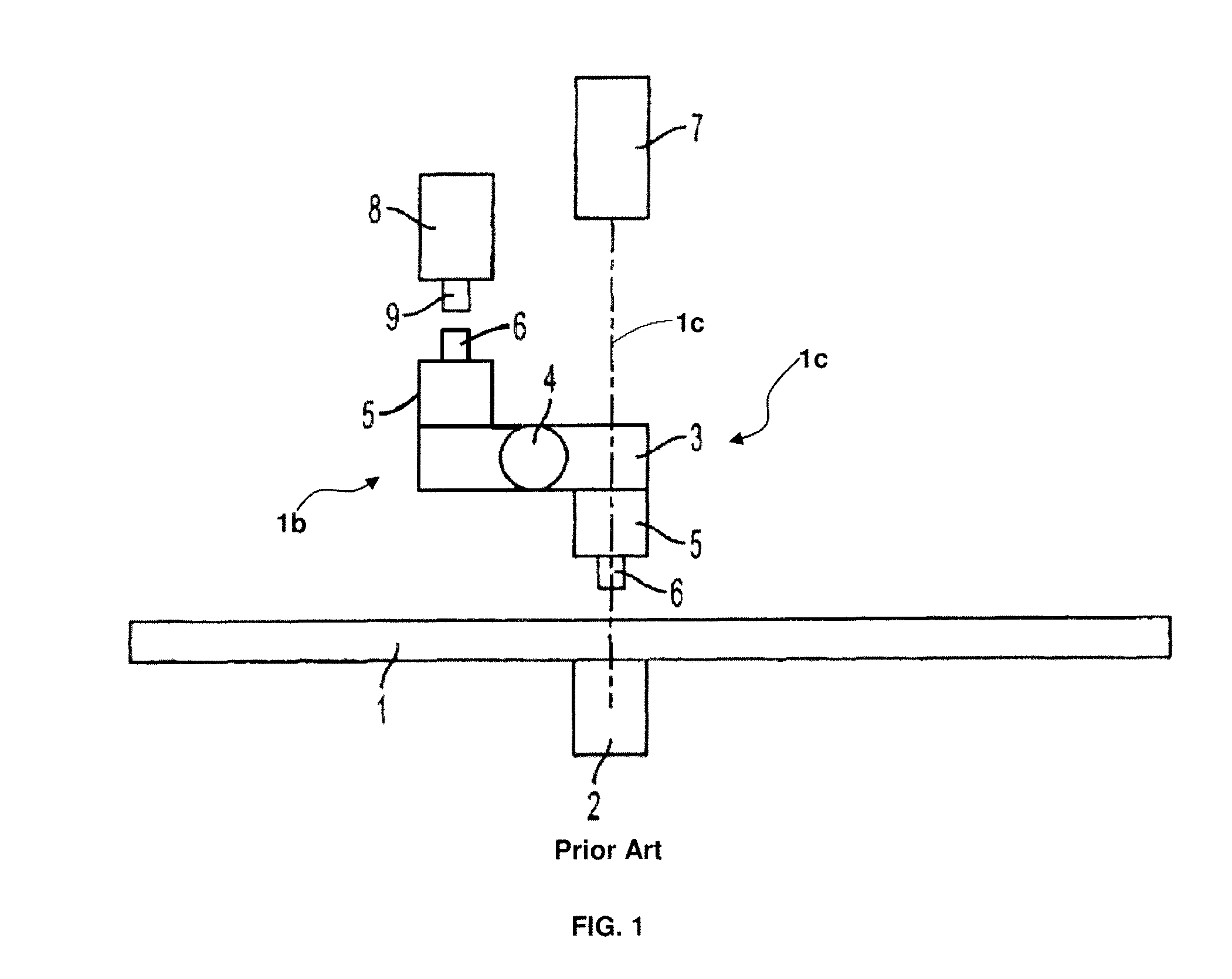
The following description relates generally to a transfer system for transferring and changing the orientation of electronic devices such as semiconductor chips, and more specifically, to a system for transferring and flipping chips that provides additional operation space and greater efficacy than conventional systems. Semiconductor device fabrication is the process used to create the integrated circuits that are present in everyday electrical and electronic devices. In typical semiconductor fabrication, integrated circuits (“ICs” or “chips”) are built in large quantities on a single large wafer of semiconductor material, typically silicon. The individual chips are patterned with small pads of metal near their edges that serve as connections to a mechanical carrier. The chips are then cut out of the wafer and attached to carriers, typically via wire bonding such as thermosonic bonding. The wires used in the wire bonding eventually lead to pins on the outside of the carriers, which are attached to circuitry making up the electronic system. A flip chip pin grid array (FCPGA) is a form of pin grid array in which the die faces downwards on the top of the substrate with the back of the die exposed. The term “flip chip” can also refer to a controlled collapse chip connection which is a method for interconnecting semiconductor devices, such as IC chips and microelectromechanical systems (MEMS), to external circuitry with solder bumps that have been deposited onto the chip pads. The process is similar to conventional integrated circuit fabrication, but includes a few additional steps. Toward the end of the manufacturing process, attachment pads are metalized to make them more receptive to solder. Metalization typically includes several treatments. A small dot of solder is deposited on each metalized pad. The chips are then cut out of the wafer. To attach the flip chip into a circuit, the chip is inverted to bring the solder dots down onto connectors on underlying electronics or a circuit board. The solder is then re-melted to produce an electrical connection, typically using a thermosonic bonding, or alternatively, a reflow solder process. During production, individual semiconductor chips are typically oriented such that their leads face away from the receiving surface. It may be necessary to “flip” the chips with a flipping mechanism before the chips are transferred for subsequent processes, such as function testing or visual integrity checking. Conventional flipping mechanisms increase the frequency by which the semiconductor packages are picked and placed, which increases the likelihood that packages are dropped and/or damaged. For example, The pivoting part 14 includes cheek projections 18 This sight channel 23 Related art US 20140328652 A1 discloses a transfer apparatus for transferring electronic devices from a wafer to a test handler. The transfer apparatus comprises a rotary device rotatable about an axis and a plurality of holders configured to hold the electronic devices for transfer from the wafer to the test handler. The holders are coupled to, and extendable from, the rotary device to pick the electronic devices from the wafer. Specifically, the plurality of holders are arranged circumferentially around, and inclined with respect to, the axis of the rotary device, so as to change an orientation of the electronic devices on the wafer to a desired orientation of the electronic devices on the test handler. Because the transfer apparatus uses a vertical wafer table, chips are prone to falling from the wafer and becoming damaged. Another related art, WO 2003058708 A1, discloses a flip bonder having a pick-up turret assembly with a number of pick-up nozzles, and a placing turret assembly with a number of placing nozzles. Each pick-up nozzle picks a die by its bumped surface, and indexes the picked die to the transfer location, thereby flipping the picked die. At the transfer location, the picked die is transferred to a placing nozzle, with die now held by its back surface. The placing nozzle is indexed to a fluxing location where flux is applied to the die, and further indexed to a placing location, where the fluxed die is placed on a target location on a lead frame, with the bumps abutting lead portions of the lead frame. The multiple nozzles allow concurrent operations with each die, thus supporting an improved throughput. However, because there is only one vertical flipper, it is only possible to have one check station. A need, therefore, exists for a system capable of quickly and accurately picking, flipping and transferring chips without dropping or damaging them. It should also provide increased operation space so that chips can be examined or checked by multiple devices such as cameras. The following summary is provided to facilitate an understanding of some innovative features and is not intended to be a full description. An appreciation of the various aspects disclosed herein can be gained by considering the specification, claims, drawings, and abstract. A transfer system for flipping and checking electronic devices includes a wafer table inclined about a first angle with respect to a horizontal axis. A first rotary device is rotatable about a second angle, and the first rotary device includes a plurality of first transfer heads circumferentially arranged around the first rotary device and inclined with respect to an axis of said first rotary device. The transfer heads are configured to pick and hold the electronic devices from the wafer table and transfer the electronic devices to a second rotary device. The second rotary device is rotatable about a vertical axis, and includes a plurality of second transfer heads vertically arranged on a circumference of the second rotary device. The rotary device is configured to pick the electronic devices from the first rotary device and transfer the electronic devices to a handling device. The transfer system further includes a first imaging device configured to inspect the electronic devices to be picked from the wafer table. A second imaging device is configured to inspect the electronic devices to be placed on the handling device. A plurality of check stations positioned around the first and second rotary devices are configured to check at least one parameter of the electronic devices held by at least one of the first and second transfer heads after picking the electronic devices from the wafer table. Each of the first transfer heads is configured to pick the electronic devices and place the electronic devices on one of the second transfer heads at an interval of 180 degrees of rotation. In one aspect, the electronic devices include semiconductor chips. In another aspect, the first angle is in the range of 1 to 89 degrees. In another aspect, the second angle is in the range of 1 to 89 degrees. In another aspect, the first imaging device includes a camera, a first light source, and a first reflecting device. In another aspect, the camera is a downward facing camera positioned above the wafer table. In another aspect, the first imaging device and the first light source are positioned along an axis of the first imaging device. In another aspect, the first reflecting device is configured to increase an inspection time of the electronic devices when picking the electronic devices from the wafer table. In another aspect, the first reflecting device is configured to reflect light from the light source to an axis of one of the transfer heads. In another aspect, the transfer system further includes at least one first suction device connected to the first transfer heads. The suction device is configured to provide suction force to each one of the first transfer heads when picking the electronic devices from the wafer table. In another aspect, the transfer system further includes at least one second suction device connected to the second transfer head. The second suction device is configured to provide suction force to each of the plurality of second transfer heads when picking the electronic devices from the second transfer heads. In another aspect, the first suction device is configured to provide sufficient suction force to hold the electronic devices during a flipping process. In another aspect, the second suction device is configured to provide sufficient suction force to hold the electronic devices during a flipping process. We also describe a transfer apparatus for flipping and checking electronic devices, comprising a wafer table for placing electronic devices, a first rotary head positioned at an acute angle the said wafer table for picking the electronic devices from the wafer, the first rotary head composed of a plurality of first transfer heads. A second rotary head is positioned substantially vertically, for picking the electronic devices from the first rotary head. The second rotary head is also composed of a plurality of second transfer heads. A handling device receives electronic devices from the second rotary head. One or more imaging devices are configured to inspect the electronic devices and one or more check stations are configured to check at least one parameter of the electronic devices. The electronic devices are rotated 180 degrees when transferred from the first rotary head to the second rotary head. The electronic devices include integrated circuits and semiconductor chips. The imaging devices can be comprised of a camera, a first light source and a first reflecting device. Further, the camera can be a downward facing camera positioned above the wafer table. The first imaging device and the first light source can be positioned along an axis of the first imaging device. A first suction device can be connected to the first transfer heads, configured to provide suction force to each of the transfer heads when picking electronic devices from the wafer table. A second suction device can be connected to the second transfer heads, configured to provide suction force to each of the second transfer heads. The summary above, as well as the following detailed description of illustrative embodiments, is better understood when read in conjunction with the appended drawings. For the purpose of illustrating the present disclosure, exemplary constructions of the disclosure are shown in the drawings. However, the disclosure is not limited to specific methods and instrumentalities disclosed herein. Moreover, those in the art will understand that the drawings are not to scale. Wherever possible, like elements have been indicated by identical numbers. The particular values and configurations discussed in the following non-limiting examples can be varied, are cited merely to illustrate at least one embodiment, and are not intended to limit the scope thereof. Without intent to further limit the scope of the disclosure, examples of instruments, apparatus, methods and their related results according to the embodiments of the present disclosure are given below. Note that titles or subtitles may be used in the examples for convenience of a reader, which in no way should limit the scope of the disclosure. Unless otherwise defined, all technical and scientific terms used herein have the same meaning as commonly understood by one of ordinary skill in the art to which this disclosure pertains. In the case of conflict, the present document, including definitions, will control. The term “ball grid array” or “BGA” as used herein, refers to type of surface-mount packaging (a chip carrier) used for integrated circuits. The term “electronic device,” as used herein, refers to a single chip or a die cut from a semiconductor wafer. The term “integrated circuit,” as used herein, refers to a small complex of electronic components and their connections that is produced in or on a small slice of material such as silicon. The term “operation space,” as used herein, refers to the space available to test, examine, photograph, alter or manipulate an electronic device during the fabrication process. The term “pick and place” or “PnP” as used herein, refers to surface mount technology (SMT) component placement systems, which are robotic machines used to place surface-mount devices (SMDs) onto a printed circuit board (PCB). The term “semiconductor chip,” as used herein, refers to an integrated circuit or monolithic integrated circuit (also referred to as an IC, a chip, or a microchip) which is a set of electronic circuits on one small plate (“chip”) of semiconductor material, normally silicon. The term “wafer table,” as used herein, refers to a type of handling system, which must reliably, securely, and selectively position and hold a wafer or chip relative to elements of a processing system. It will be appreciated that terms such as “front,” “back,” “top,” “bottom,” “side,” “short,” “long,” “up,” “down,” and “below” used herein are merely for ease of description and refer to the orientation of the components as shown in the figures. It should be understood that any orientation of the components described herein is within the scope of the present invention. Other technical terms used herein have their ordinary meaning in the art that they are used, as exemplified by a variety of technical dictionaries. The invention includes a transfer system for flipping and checking electronic devices. The design presents several advantages over conventional systems including:
In one embodiment, the first angle ranges from 1 to 89 degrees, preferably between 10 and 84 degrees, or more preferably 30 degrees. The angle of the wafer table is an important consideration for optimal use of the system. With a higher angle (more vertical), the electronic device is more likely to fall. With a lower angle there is less operation space. For example, with an angle of 45 degrees from horizontal, the wafer table may not be able to support the weight of the electronic device. When the first angle is between 35 degrees and 40 degrees, the electronic device can slip. When the angle is below 30 degrees, there is less operation space for arranging the devices used for flipping and checking the electronic devices. Hence, an optimal first angle is 30 degrees. In another embodiment, the second angle ranges from 1 to 89 degrees. Although the embodiment of the first rotary device shown in According to the embodiments shown in It should be noted that to flip the electronic devices, each first transfer head is rotated 180 degrees after picking the electronic devices. Furthermore, the electronic device 43 is placed at 180 degrees on the second transfer head 36 of the second rotary device. As shown in In one embodiment, the check station 24 is arranged in front of the second transfer head 37. As shown in The second rotary device 50 may be a Pick and Place (PnP) turret with six transfer heads, although other devices may also be used without limitation. The check station 22, 23 and 24 may comprise one or more sensors, cameras, and the like, to check at least one parameter of the electronic device. As shown in the embodiment of The camera 26 is configured to image the electronic device from above when the wafer table is picked for inspection. In one embodiment, the first reflecting device 28 is a mirror. However, other reflecting devices can also be used without limitation. Similar to the first imaging device 64, the transfer system 70 can also have a second imaging device 25. The second imaging device 25 can include a camera, which may be, for example, an upward facing camera configured to inspect the flipped electronic device placed on the handling device 60. In one embodiment, the second imaging device 25 also includes at least one light source, at least one reflecting device, and at least one camera. The first imaging device 64 and the second imaging device 25 can include any number of cameras. In one embodiment, at least one downward facing camera is used to check the position of the electronic device to facilitate picking the electronic device. If one of the first transfer heads 30, 31, 32, 33, 34 or 35 is set to be a check station, then there can also be a camera for that station. In one embodiment, the first imaging device 64 and the second imaging device 25 act as a check station. Images obtained from the cameras of the check station can be used to detect the position of the chip on the check station for adjustment before placing the electronic device into the handling device. The images can also be used to test a weld ball on a top face of the electronic device (die) or the side face of the electronic device (die), etc., without limitation. In one embodiment, each first transfer head 30, 31, 32, 33, 34 and 35 is connected to a first suction device 29 to provide controlled suction force for picking the electronic device 40, 41, 42 or 43 from the wafer table 21. The first suction device 29 allows the respective first transfer heads 30, 31, 32, 33, 34, and 35 to hold the electronic device 40, 41, 42 or 43 during 180 degree rotation and also provides force necessary to place the electronic device 40, 41, 42 or 43 on the second transfer head 36, 37, 38 or 39 of the second rotary device 50 during the flipping process. The suction force can be created by a vacuum. The transfer system 70 can be controlled by a controller (not shown) via manual operation or software to perform flipping and checking of the electronic devices 40, 41, 42 and 43. The inclined first rotary device 20 and inclined wafer table 21 increase the operation space of the transfer system 70. The inclined first rotary device 20 can be configured to provide space for multiple checking stations 22, 23 and 24 during flipping, or index rotation, of the electronic device 40, 41, 42 or 43, and allow the operator to clearly and easily observe the operating condition of the transfer system 70. As the transfer system 70 uses two rotary devices 20 and 50 with multiple transfer heads, the flipping process can be performed at higher speeds, which in turn increases the UPH. The inclined wafer table 21 provides space for the first imaging device 64, such that the first light source 27 and the first reflecting device 28 increase the inspection time of the electronic devices 40, 41, 42 or 43 when picking from the wafer table 21. It should be noted that in one embodiment, the wafer table 21 is oriented at an angel (α°) from horizontal, as depicted in It will be appreciated that variations of the embodiments disclosed above and other features and functions, or alternatives thereof, may be combined into many other different systems or applications. It will also be appreciated by those skilled in the art that various other modifications, variations or improvements may be made. Although the embodiments set forth in the current disclosure have been described in considerable detail to cover certain aspects, those skilled in the art will recognize that other versions of the embodiments set forth herein are also possible. The present invention includes a transfer system for flipping and checking electronic devices. A first rotary device has a plurality of transfer heads configured to pick electronic devices from a wafer table and place the electronic devices on a transfer head of a second rotary device. Check stations can be positioned around the first and second rotary devices and configured to inspect or check the electronic devices during the flipping process. The transfer system can further include an imaging device to inspect the accuracy of picking and placing of the electronic devices during the flipping process. The wafer table and the first rotary device are inclined to increase the operation space. The system accurately picks, flips and transfers chips at a high operation speed. 1. A transfer system for flipping and checking electronic devices, said transfer system comprising:
a wafer table inclined about a first angle with respect to a horizontal axis; a first rotary device positioned at a second angle with respect to a horizontal axis, said first rotary device comprising a plurality of first transfer heads circumferentially arranged around said first rotary device, said first transfer heads configured to pick and hold said electronic devices from said wafer table and transfer said electronic devices to a second rotary device; the second rotary device being rotatable about a horizontal axis, said second rotary device comprising a plurality of second transfer heads vertically arranged on a circumference of said second rotary device, said second rotary device configured to pick said electronic devices from said first rotary device and transfer said electronic devices to a handling device; a first imaging device to inspect said electronic devices to be picked from the wafer table; a second imaging device to inspect said electronic devices to be placed on the handling device; a plurality of check stations positioned around said first and second rotary devices, said plurality of check stations configured to check at least one parameter of said electronic devices held by at least one of said first and second transfer heads; and wherein said wafer table is at a substantially right angle with respect to the axis of said first transfer heads. 2. The transfer system of 3. The transfer system of 4. The transfer system of 5. The transfer system of 6. The transfer system of 7. The transfer system of 8. The transfer system of 9. The transfer system of 10. The transfer system of 11. The transfer system of 12. The transfer system of wherein the first suction device is configured to provide sufficient suction force to hold said electronic devices during a flipping process. 13. The transfer system of wherein the second suction device is configured to provide sufficient suction force to hold said electronic devices during a flipping process. 14. (canceled) 15. (canceled) 16. An apparatus for transferring electronic devices, comprising:
a. a wafer table for placing and storing electronic devices, said wafer table positioned at a 30 degree angle below horizontal; b. a first rotary head positioned at a 90 degree angle from the wafer table for picking electronic devices from the wafer table, said first rotary head composed of a plurality of first transfer heads positioned around the circumference of the first rotary head; c. a second rotary head positioned horizontally, for receiving electronic devices from the first rotary head, said second rotary head composed of a plurality of second transfer heads positioned around the circumference of the second rotary head; d. a handling device for receiving electronic devices from said second rotary head; e. one or more imaging devices configured to inspect the electronic devices; and f. one or more check stations configured to check at least one parameter of the electronic devices, wherein said electronic devices are flipped 180 degrees when transferred from said wafer table to said second rotary head. 17. (canceled) 18. The apparatus of 19. The apparatus of 20. The apparatus of 21. The apparatus of 22. The apparatus of 23. The apparatus of FIELD OF THE INVENTION
BACKGROUND
SUMMARY OF THE INVENTION
BRIEF DESCRIPTION OF THE DRAWINGS
DETAILED DESCRIPTION OF THE INVENTION
Description of Preferred Embodiments