SINGLE-ENDED CURRENT SENSE AMPLIFIER
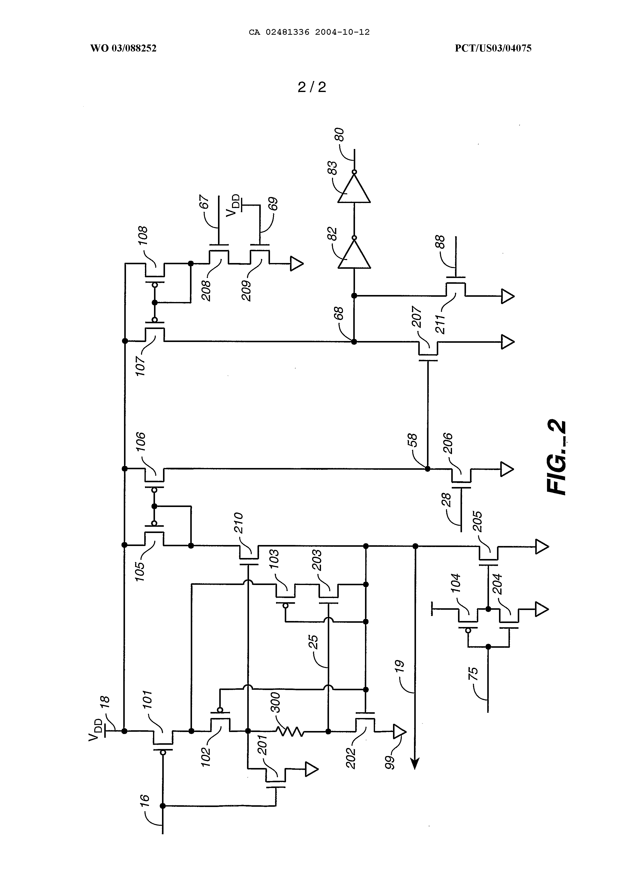
WO 03/088252 PCT7US03/04075 SINGLE-ENDED CURRENT SENSE AMPLIFIER TECHNICAL FIELD The present invention relates to sense ampli¬ fier circuits for use in memory integrated circuits. BACKGROUND ART In memory integrated circuits, sense amplifiers are used to detect and determine the data content of a selected memory cell. In EEPROM (Electronically Erasable Programmable Read Only Memories) and Flash memories, the sense amplifier serves two functions. Firstly, the sense amplifier précharges the bitline to a clamped value, and secondly, it senses the current flowing into the bitline, which depends on the memory cell state. Both the reli¬ ability, in terms of endurance and retention, and the performance depend to greatly on the design of the sense amplifier. The majority of integrated sense amplifier structures are based on a differential amplifier being used to compare the current coming from the selected memory cell to the current of a reference cell. The reference cells can be implemented in different ways, and are of different types. The reference cells are pro¬ grammed one time only during the test of the memory, thus increasing the testing time. In order to ensure the good functionality of the sense amplifier, the ratio Icell/Iref must be maintained high enough to take into account the process fluctuations on the memory and the reference cells, and the impact of the memory cycling on the memory cells. Moreover, it has been shown that the speed performance and reliability of the standard differ¬ ential amplifier sense amplifiers are highly reduced for supply voltage values under 2V. Other types of sense amplifier structures are non-differential types that have nonsymmetrical circuits WO 03/088252 PCT7US03/04075 which detect and amplify signals which are generated by an accessed memory cell on a single amplifier input node. These types of sense amplifiers are often referred to as "single-ended". Among the single-ended sense amplifiers of the prior art is U.S. Pat. No. 4,918,341 to Galbraith et al. which discloses a single-ended sense amplifier that includes a complementary current mirror circuit that converts a single-ended input current into a single-ended output voltage. The x341 patent also discloses a circuit for filtering high frequency noise spikes. U.S. Pat. No. 5,013,943 to Hirose discloses a single-ended sense ampli¬ fier having a precharging circuit in order to lessen the effect of changing the bitline capacitance and the vari¬ ability in the current conducted by the cell. U.S. Pat. No. 5,666,310 to Yu et al. discloses a sense amplifier circuit that senses the current drawn by the memory array and changes the state of the output once a certain cur¬ rent has been reached. The trend in recent years is to design memory circuits that consume less power. One way to do this is to decrease the voltages of the power supplies that pro¬ vide power to the memory. As the power supply voltages used for sense amplifiers decrease, it becomes more im¬ portant that the sense amplifier be able to sense very low current levels. It is the object of the present invention to provide a single-ended sense amplifier having direct current amplification in order to sense very low cur¬ rents . It is a further object of the invention to provide a single-ended sense amplifier that can be de¬ signed using standard low voltage CMOS devices. SUMMARY OF THE INVENTION The above objects have been achieved by a single-ended current sense amplifier having a précharge circuit to maintain a stable voltage on a bitline, a sensing circuit coupled to the bitline for sensing an WO 03/088252 PCT7US03/04075 amount of current flowing into the bitline, a direct current amplification circuit coupled to the sensing circuit for amplifying the current sensed on the bitline, a current-to-voltage conversion circuit for converting the sensed current to a voltage, and a voltage amplifica¬ tion circuit for amplifying the voltage at the sense amplifier output. The sense amplifier also includes an overshoot filtering circuit to filter out positive glitches on the bitline. The single-ended structure provides the advan¬ tage of eliminating the need to have a reference cell and a comparator circuit as are commonly used in the differ¬ ential sense amp structures. This provides a savings in testing time and in the amount of die area used by the sense amplifier circuit. Additionally, the single-ended structure provides other advantages over the standard differential structures such as providing less sensitiv¬ ity to mismatching and process variations and providing improved access time at low supply voltages. By providing direct current amplification imme¬ diately following the current sensing, the sense ampli¬ fier of the present invention is faster and can sense very low currents compared to other single-ended sense amplifiers of the prior art. BRIEF DESCRIPTION OF THE DRAWINGS Fig. 1 is a block diagram of the structure of the sense amplifier circuit of the present invention. Fig. 2 is an electrical schematic diagram of the sense amplifier circuit of Fig. 1. BEST MODE FOR CARRYING OUT THE INVENTION With reference to Fig. 1, the sense amplifier of the present invention includes a précharge circuit 20, which functions to précharge and maintain a stable volt¬ age on the bitline 19. The précharge circuit 2 0 receives a power supply voltage Vdd 18 at an input terminal and a sense on/off signal 16 at another input terminal to acti- WO 03/088252 PCT7US03/04075 vate the sense amplifier circuit. A sensing circuit is coupled to the bitline 19 and is used to sense the current flowing into the bitline. An overshoot filtering circuit 7 0 is coupled to the sensing circuit 30 in order to filter out positive glitches on the bitline. The output of the sensing circuit 30 goes to a direct current amplification circuit 40 which amplifies the current that was sensed by the sensing circuit. The amplified current is converted into a voltage by the current-to-voltage conversion circuit 5 0 and then the resulting voltage is amplified by the output amplification stage 60 and is provided to the sense amplifier output 80. With reference to Fig. 2, the précharge circuit consists of transistors 101, 102, 103, 202, 203 and re¬ sistor 3 00. Transistors 101, 102 and 103 are PMOS type transistors while transistors 2 02 and 2 03 are MMOS type transistors. Transistor 101 has a gate input connected to the sense amplifier on/off signal input terminal 16, a source terminal coupled to the power supply voltage Vdd 18, and a drain terminal connected to the source terminal of PMOS transistor 102. Transistor 102 has a drain ter¬ minal coupled to the first end of resistor 300, and a gate terminal coupled to the gate of transistor 202. Transistor 2 02 has a drain terminal connected to the second end of resistor 300 and a source terminal con¬ nected to ground potential 99. Transistor 103 has a gate terminal connected to the gate terminal of transistor 2 02, a source terminal connected to the drain terminal of transistor 101, and a drain terminal connected to the drain of transistor 2 03. Transistor 2 03 has a source terminal connected to the gate of transistor 202 and a gate terminal connected between the drain terminal of transistor 202 and the second end of resistor 300. The précharge circuit functions to précharge and maintain a stable voltage on the bitline 19. The bitline 19 is connected to the source terminal of transistor 203, as shown in Fig. 2. The branch consisting of transistors 101, 103 and 2 03 must drive enough current to set the WO 03/088252 PCT7US03/04075 bitline 19 to its clamped voltage in a limited amount of time. The clamped précharge voltage is determined by the sizing of transistors 102 and 2 02 and the size of the resistor 300. When the bitline reaches the trip point of the 102, 202 and the resistor 300 stage, the bias low line 25 goes low, turning off transistor 203, and thus turning off the précharge branch. The sensing circuit consists of NMOS transistor 210, and PMOS transistors 105 and 106. Transistor 210 has a gate terminal connected to the drain terminal of transistor 2 01, a drain terminal connected to the drain terminal and gate terminal of transistor 105 and to the gate terminal of transistor 106, and a source terminal connected to the bitline. Transistors 105 and 106 have gate terminals connected to the drain terminal of 105, and source terminals connected to the power supply volt¬ age Vdd. The drain terminal of transistor 106 is con¬ nected to the drain terminal of NMOS transistor 206. Transistor 206 has a gate terminal 28 connected to a sense mode enable signal, and a source terminal connected to a ground potential. Transistor 210 serves to isolate the bitline voltage from the gate level of transistor 105, which allows the potential on the bitline to be imposed by the précharge circuit. Transistor 106 mirrors the cell current multiplied by a factor of N. Thus, the cell current is directly amplified and is supplied to the drain of the low drive 2 06 transistor, resulting in current-to-voltage conversion and a first voltage VI at node 58. Transistor 206 has a low W/L value and the current trip point of the sense amplifier can be adjusted by varying the multiplication factor N and the size of the transistor 206. The converted voltage VI is amplified by the voltage amplification circuit consisting of PMOS transis¬ tors 107 and 108, and NMOS transistors 2 07, 2 08 and 2 09. Transistor 107 has a source terminal connected to the power supply voltage Vdd 18 and a drain terminal con¬ nected to the drain terminal of transistor 2 07. Transis- WO 03/088252 PCT7US03/04075 tor 2 07 has a gate terminal connected to node 58 to re¬ ceive the voltage VI, and a source terminal connected to a ground potential. Transistors 107 and 207 amplify the voltage VI to produce an amplified voltage V2 at a node 68. Transistors 108, 208, and 209 act as a bias current generator. Transistor 2 08 has a source terminal con¬ nected to the power supply voltage Vdd 18, and a gate terminal connected to its drain terminal and also to the gate terminal of transistor 107. Transistor 208 has a drain terminal connected to the drain terminal of tran¬ sistor 108, and a gate terminal 67 connected to a sense mode enable signal. Transistor 209 has a drain terminal connected to the source of transistor 2 08, a gate termi¬ nal 69 connected to a power supply voltage Vdd and a source terminal connected to a ground potential. The bias current generator generates a bias current which is supplied through transistor 207 to the node 68. The voltage V2 goes through a pair of inverters 82, 83, serv¬ ing as output buffers, and the output of the sense ampli¬ fier is produced at terminal 80. NMDS Transistors 201 and 211 are used to turn the sense amplifier off in stand by mode, or in the mode where there is no DC current. Transistor 201 has a drain terminal connected to the gate terminal of transistor 210 and to the source terminal of transistor 102 and to the first end of resistor 300. Transistor 201 also has a source terminal connected to ground potential, and a gate terminal 88 connected to sense on/off signal input termi¬ nal. Transistor 211 has a drain terminal connected to node 68, a source terminal connected to ground potential, and a gate terminal 88 connected to the sense on/off signal. Additionally, the sense amplifier also includes an overshoot filtering circuit consisting of PMOS tran¬ sistor 104 and NMOS transistors 204 and 205. Transistors 104 and 2 04 are connected as an inverter with the source of transistor 104 being connected to a power supply Vdd, the drain of 2 04 being connected to the drain of transis- WO 03/088252 PCT7US03/04075 tor 204, the source of transistor 204 being connected to a ground potential, and the gates of transistors 104 and 2 04 being connected together and being supplied with a bias high signal at the gate terminal 75. The output of the 104, 2 04 inverter is connected to the gate of tran¬ sistor 205. Transistor 205 has a drain terminal con¬ nected to the bitline 19 and a source terminal connected to the ground potential. Due to the sense environment, overshoots can occur on the bitline that can affect the normal sensing operation. The overshoot filtering cir¬ cuit serves to filter positive glitches on the bitline. In the case of a positive glitch on the bitline, the bias high signal goes low which produces a high signal at the output of inverter 104, 204. This high signal turns on transistor 2 05 which discharges the glitch. Compared to the usual prior art structures that use a transistor in diode, this solution has the advantage to drive current in the transistor 2 05 only if there is an overshoot on the bitline 19. The following is the description of the circuit according to the inputs. When the sense on/off signal 16 is off, the sense on/off signal is set high while the sense mode enable signal 2 8 is set low. The high sense mode enable signal turns on transistor 211, placing a low potential on node 68, and setting the output 80 of the sense amplifier to a low state. In this situation, there is no DC current in the structure. When the sense on/off signal is on, meaning that DC current is flowing, the sense on/off signal goes low and the sense mode enable signal goes high. The low signal turns on transistor 101 and turns off transistor 201. This allows current to flow through transistors 103, 2 03 and 210 and thus start the précharge circuit. As explained above, the précharge circuit will set the bitline 19. In order to read an ON cell, or a "0", transis¬ tor 2 06 must drive a large current equal to the current generated from the drain of transistor 106 in order for the voltage VI at its drain to rise. The variation of WO 03/088252 PCT7US03/04075 voltage VI is then amplified by the voltage amplification circuit (transistors 107 and 207) and the output voltage V2 at node 68 quickly goes low, providing a low signal, or "0", on the sense amplifier output 80. In order to read a OFF cell, or a "1", the transistor 206 has no current to drive so the voltage VI at node 58 goes low. This turns off transistor 207 and the voltage V2 at node 68 increases strongly, producing a high output at the sense amplifier output 80. The sizing of the sense amplifier will be driven by two objectives, the first objective is to meet the targeted current trip point limit. This is obtained through a DC analysis. The second objective is to achieve the performance target in terms of access time and power. To determine these objectives, a first order modeling of the structure is needed. This first order modeling is described herein. The first step in this process is to use DC modeling to calculate the current trip point. The sense amplifier switches from 1 to 0 when node 58 reaches the output stage trip point. For the purpose of simplifica¬ tion, an assumption is made that the output stage trip point is equal to the threshold voltage (VTN) of transis¬ tor 207. When VI varies from 0 to VTN, transistor 206 is in linear mode, acting as a resistance. The condition to determine the current trip point limit (Ilim) is as fol¬ lowing : R206nIlim=VTNwhereR206 = ii cox — \yDD-vTN) V L ) 206 giving the following expression for Ilim: 1 (W\ ( \ V J 206 WO 03/088252 PCT7US03/04075 - y - This expression exhibits a linear variation with respect to VDD. As the mobility \i and threshold voltage VTN decrease with temperature, a decrease of Ilim with temperature is expected. Finally, it appears clearly that the current trip point can be fixed by tun¬ ing the multiplication factor n of the current mirror and the sizing of the transistor 206. Next, dynamic analysis is used to calculate the switching time. Both falling delay (reading an ON memory that drives loNiim) ani rising delay (reading an OFF cell that drives IoffhiJ must be considered for the dynamic analysis. The total switching delay can be divided into four contributions: the précharge delay, the time neces¬ sary to start the current mirror, the time necessary to charge/discharge the node 58 (VI), and the time needed to charge/discharge the node 68 (V2). For reasonable multi¬ plication factor values (n<3), the current mirror start¬ ing time is negligible. The assumption is made that the voltage V2 at node 68 is the output of the sense, the delay in the output buffers 82, 83 being negligible. When reading an ON memory cell, the voltage VI at node 58 is charged through the unbalance current nl0n- I206, and the voltage V2 at node 68 is discharged through the unbalance current l207~Ibias- So t*16 read On cell delay can be written as: IrdON ~tprécharge + 10207 "*" parl ) r _r + [ INV1 par! ) r _j where tprecharge is the précharge delay that can be adjusted by sizing the transistors 103 and 2 03, CG207 is the gate capacitance of transistor 2 07, CINV1 the input capacitance of inverter 82, Cparl is the total parasitic capacitance on node 58, including the drain capacitance of transis¬ tors 206 and 106 as well as the routing, and Cpar2 is the total parasitic capacitance on node 68 including the drain capacitance of transistors 2 07 and 107, as well as WO 03/088252 PCT7US03/04075 ' the routing. I206 and I207 are the current flowing through transistors 206 and 207 respectively. When reading an OFF memory, the VI node 58 is discharged through the current I206' while the V2 node 68 is charged through the current Ibias. More precisely, when VI switches from VDD to VTN the output voltage V2 starts rising due to the unbalance current Ibias - IN7. This is neglected for the first order modeling. The read OFF cell delay can be written as : Vnn-V™ /_ _ \VDD/2 t -t 4-(r xr \ DD TN -i. (r + r )— lrd0FF ~lprechuge r luG207 parl ) j T %%DESCRIPTION%% INV1 T u par! ) j 1 206 1 bias These equations give an indication on how the sense must be sized: First, adjust factor n and the length of the minimum width transistor 206 in order to meet the trip point target. Then, decrease the dimen¬ sions of INVl 82 in order to minimize the capacitance on V2 node 68 (CINV1) . Then, size transistor 207 and Ibias in order to minimize and balance the read ON and read OFF cell delays. In order to limit the capacitance on VI node 58, transistor 207 must be sized as small as possi¬ ble. The above described sense amplifier provides many advantages including a high robustness to process variations, improved access time at low power supply voltages, and a full and easy implementation using low voltage CMOS devices. WO 03/088252 PCT7US03/04075 A single-ended sense amplifier (Fig. 1) having a precharge circuit (20) for maintaining a stable voltage on a bitline (19), a sensing circuit (30) coupled to the bitline (19) for sensing an amount of current flowing into the bitline (19), a direct current amplification circuit (40) electrically coupled to the sensing circuit (30) for amplifying the current sensed on the bitline (19), a current-to-voltage conversion circuit (50) for converting the sensed current to a voltage and a voltage amplification circuit (60) for amplifying the voltage at the sense amp output (80). The sense amplifier can be implemented using standard CMOS components (Fig. 2) and provides improved access time at low power supply voltage, high robustness to process variations, and the ability to sense very low currents. 1. A current sense amplifier comprising:
a précharge circuit receiving an activation signal and a first power supply voltage and producing a précharge voltage on a bitline; a sensing circuit coupled to the bitline and having means for sensing an amount of current flowing into the bitline; a current amplification circuit electrically coupled to the sensing circuit and having means .for amplifying the current sensed on the bitline; a current-to-voltage conversion circuit electrically coupled to the current amplification circuit and having means for converting the sensed current to a first voltage; and a voltage amplification circuit electrically coupled to the current-to-voltage conversion circuit and having means for amplifying the first voltage to produce a second voltage at a sense amplifier output. 2. The sense amplifier of Claim 1 further including means for isolating the précharge voltage on the bitline from the sensing circuit. 3. The sense amplifier of Claim 1 further comprising an overshoot filter circuit coupled to the bitline, said overshoot filter having means for filtering glitches on the bitline. 4. The sense amplifier of Claim 3 wherein the overshoot filter includes a first inverter which receives a bias signal indicating a glitch at an input and produces an inverted bias signal at an output, and a discharge transistor having a gate terminal electrically coupled to the output of the first inverter, a drain terminal electrically coupled to the bitline and a source terminal electrically coupled to a ground potential.
WO 03/088252 PCT7US03/04075 5. The sense amplifier of Claim 1 wherein the précharge circuit clamps the précharge voltage on the bitline to a value that is lower than the value of the first power supply. 6. The sense amplifier of Claim 1 further including a first input terminal for receiving the activation signal and a second input terminal for receiving the first power supply voltage. 7. The sense amplifier of Claim 6 wherein the précharge circuit includes:
a first resistor; a first PMOS transistor (101) having a gate electrically coupled to the first input terminal and a source terminal electrically coupled to the second input terminal; a second PMOS transistor (102) having a source terminal electrically coupled to the drain terminal of the first PMOS transistor, and a drain terminal electrically coupled to a first end of the first resistor; a first NMOS transistor (202) having a gate terminal electrically coupled to the bitline, a drain terminal electrically coupled to a second end of the first resistor and a source terminal electrically coupled to a ground potential; a third PMOS transistor (103) having a gate terminal electrically coupled to the bitline, and a source terminal electrically coupled to the drain terminal of the first PMOS transistor; and a second NMOS transistor (203) having a source terminal electrically coupled to the bitline, a gate terminal electrically coupled to the second end of the first resistor, and a drain terminal electrically coupled to the drain terminal of the third PMOS transistor.
WO 03/088252 PCT7US03/04075 8. The sense amplifier of Claim 6 wherein the sensing and current amplification circuits include:
a third input terminal for receiving a sense mode enable signal; a fourth PMOS transistor (105) having a source terminal electrically coupled to the second input terminal; a fifth PMOS transistor (106) having a source terminal electrically coupled to the second input terminal, a gate terminal electrically coupled to the gate terminal of the fourth PMOS transistor, and a drain terminal electrically coupled to a first voltage node (58; VI); a third NMOS transistor (206) having a gate terminal electrically coupled to the third input terminal, a source terminal electrically coupled to the ground potential, and a drain terminal electrically coupled to the first voltage node; a fourth NMOS transistor (210) having a drain terminal electrically coupled to the drain terminal of the fourth PMOS transistor, a source terminal electrically coupled to the bitline; and a fifth NMOS transistor (201) having a drain terminal electrically coupled to the gate of the fourth NMOS transistor, a source terminal electrically coupled to the ground potential, and a gate terminal electrically coupled to the first input terminal to receive the activation signal. 9. The sense amplifier of Claim 6 wherein the voltage amplification circuit includes:
a bias current generator circuit; a sixth NMOS transistor (207) having a gate terminal electrically coupled to a first voltage node (58; VI), a source terminal electrically coupled to a ground potential, and a drain terminal electrically coupled to a second voltage node (68); WO 03/088252 PCT7US03/04075 a sixth PMOS transistor (107) having a source terminal electrically coupled to the second input terminal, a gate terminal electrically coupled to the bias current generator circuit, and a drain terminal electrically coupled to the second voltage node. 10. The sense amplifier of Claim 9 wherein the bias current generator circuit includes :
a fourth input terminal for receiving a sense mode enable signal; a seventh PMOS transistor (108) having a drain terminal, a source terminal electrically coupled to the second input terminal, and a gate terminal electrically coupled the a drain terminal; a seventh HMOS transistor (208) having a source terminal, a drain terminal electrically coupled to the drain terminal of the seventh PMOS transistor, and a gate terminal electrically coupled to the fourth input terminal; and an eighth NMOS transistor (209) having a drain terminal electrically coupled to the source terminal of the seventh NMOS transistor, a gate terminal electrically coupled to the second input terminal, and a source terminal electrically coupled to a ground potential. 11. The sense amplifier of Claim 9 wherein the voltage amplification circuit further includes a plurality of inverters electrically coupled between the second voltage node and the sense amplifier output. 12. The sense amplifier of Claim 9 further including a ninth NMOS transistor (211) having a gate terminal electrically coupled to the first input terminal, a drain terminal electrically coupled to the second voltage node, and a source terminal electrically coupled to the ground potential.