DEVICE OF MEMORY HAS SEMICONDUCTOR INCLUDING/UNDERSTANDING WAYS OF EXIT OF DATA FOR RAPID ACCESS
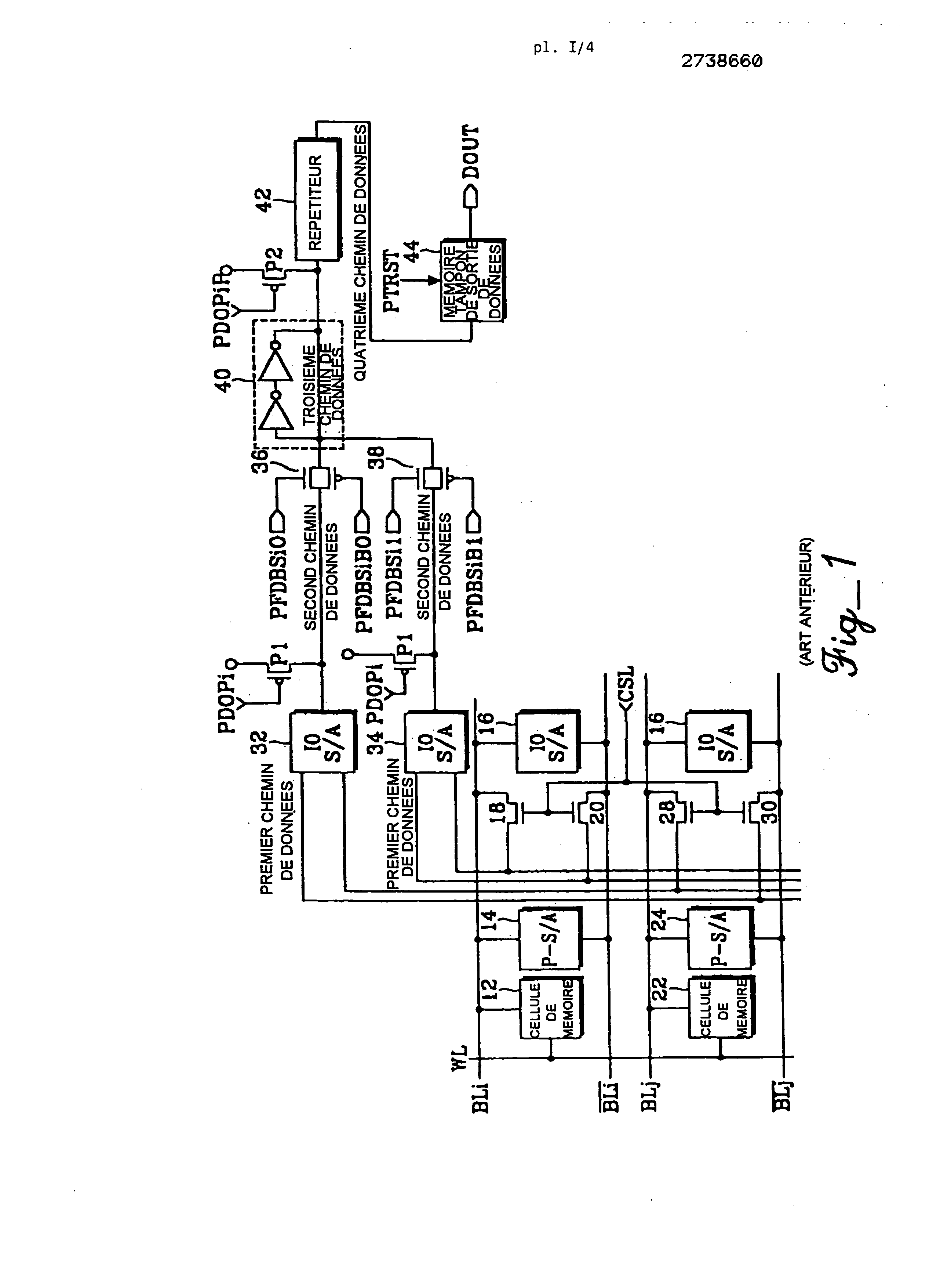
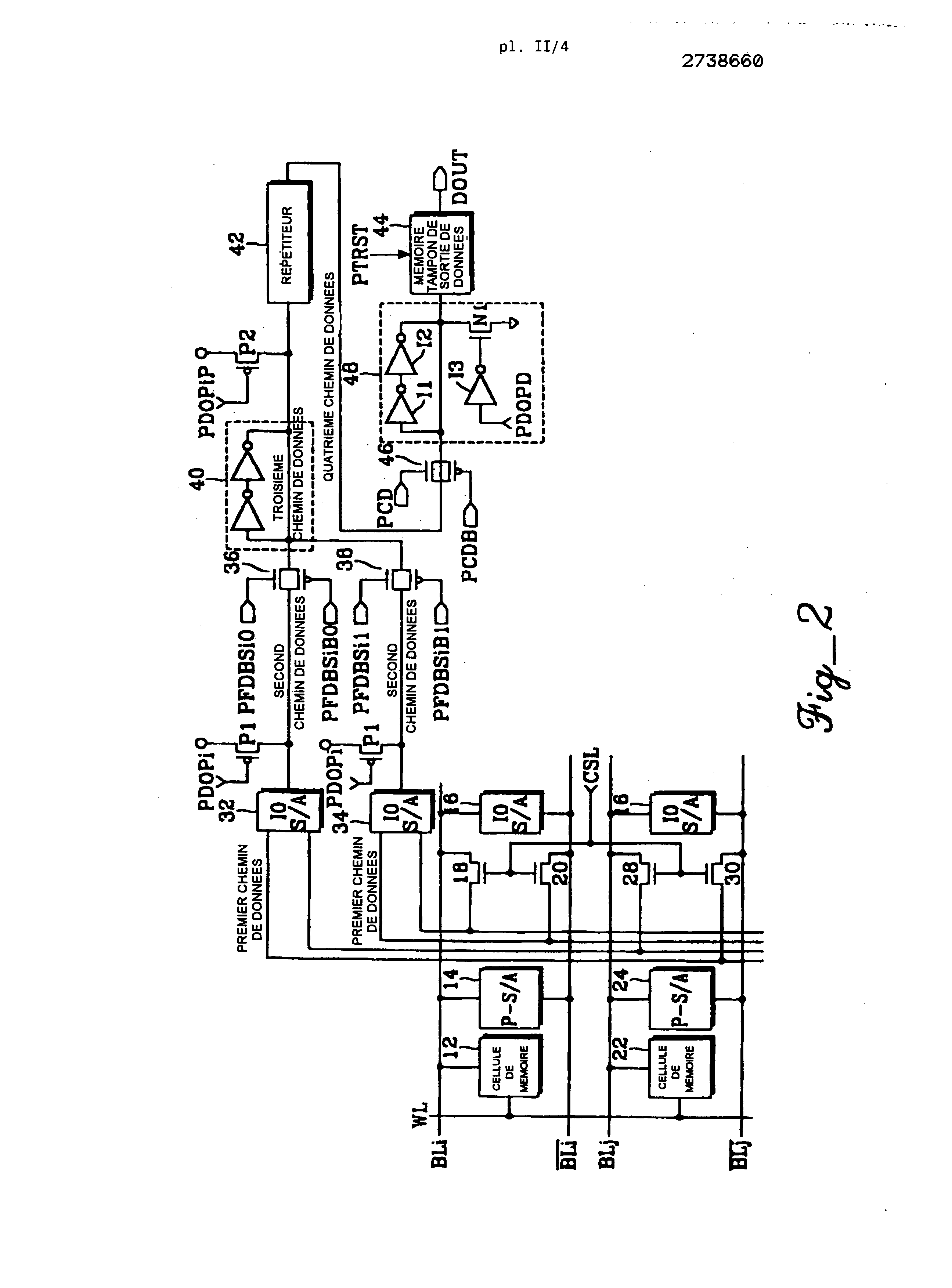
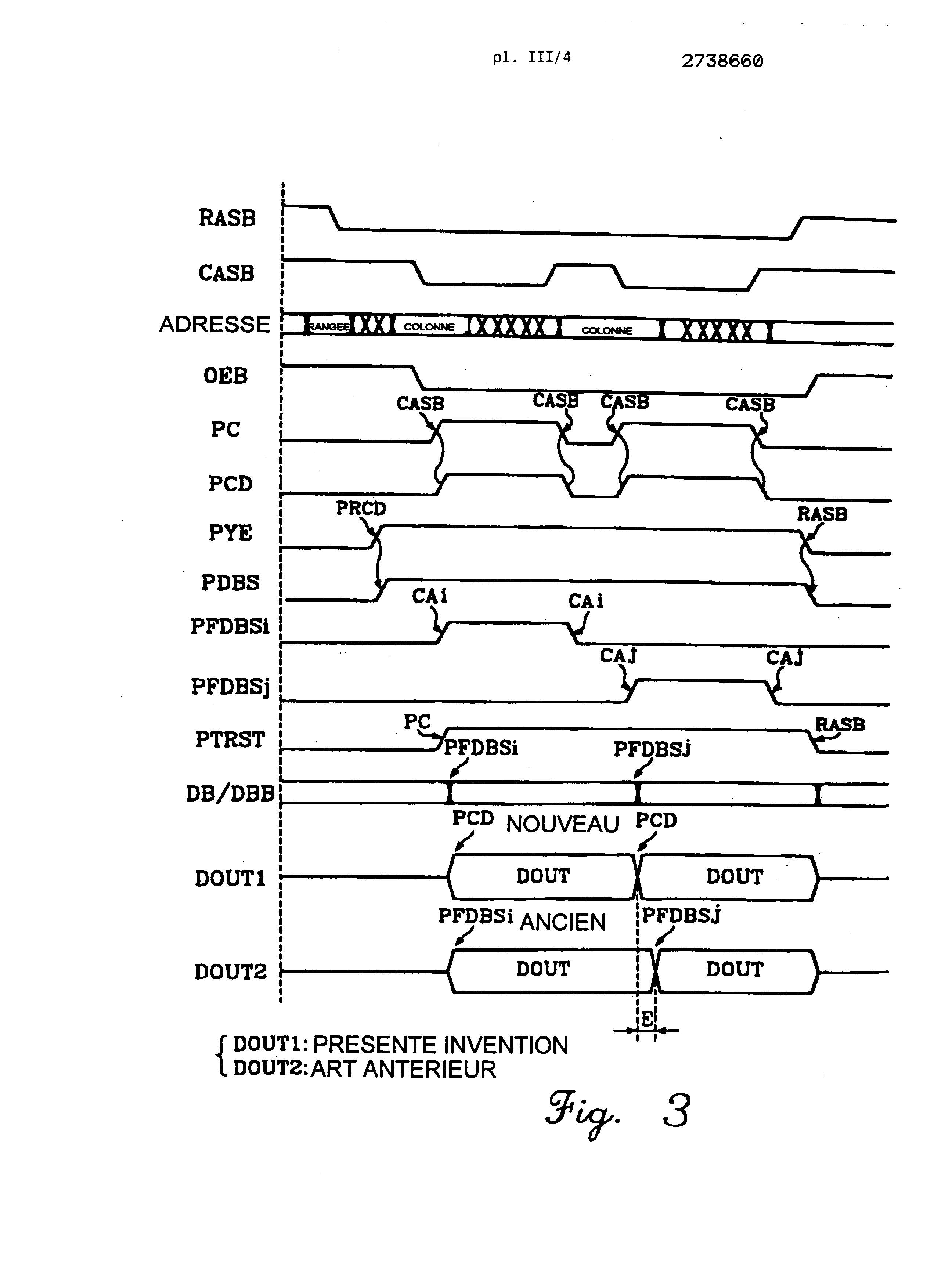
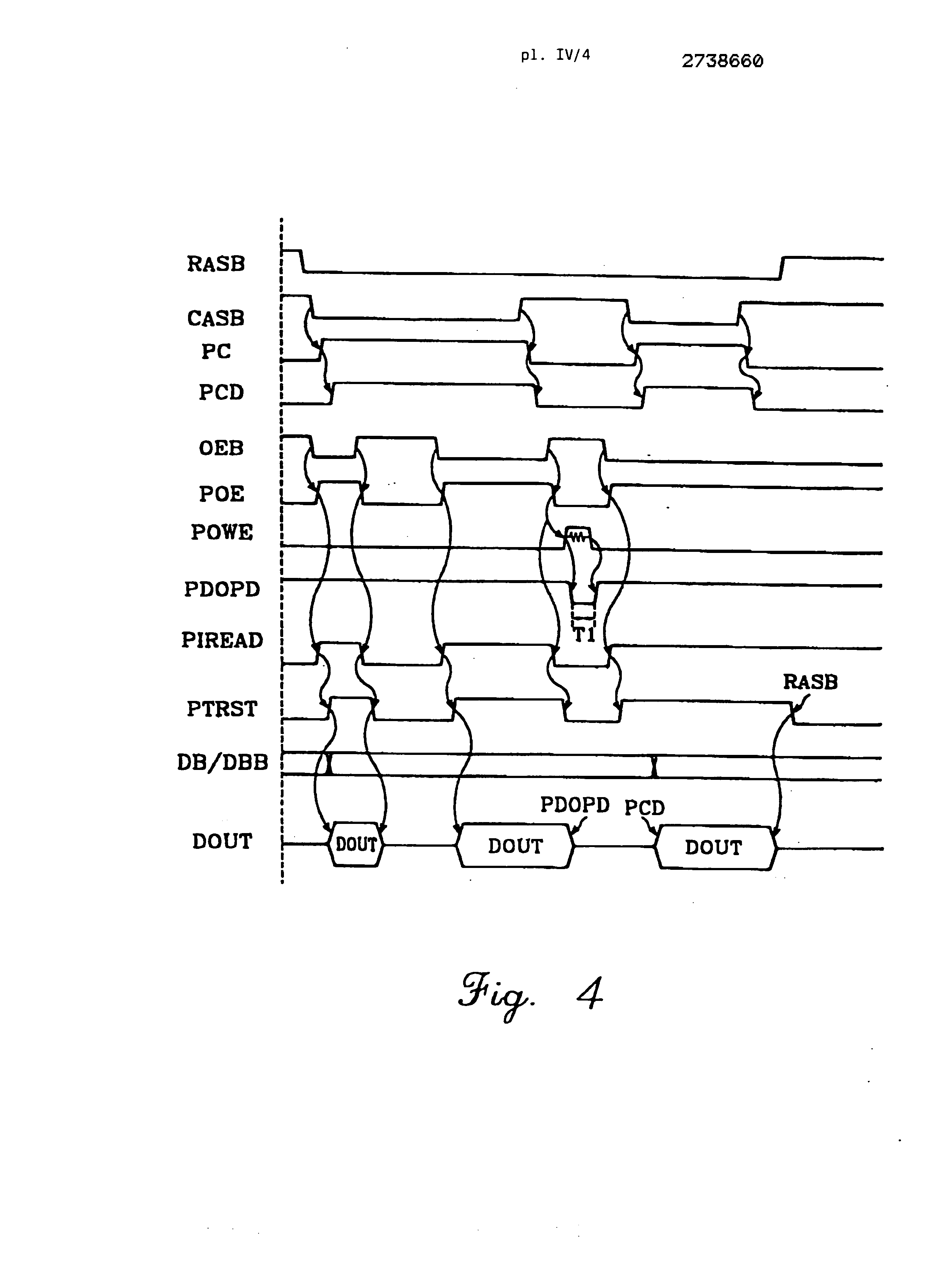
1. Field1 1 invention A semiconductor memory device and, more particularly, a semiconductor memory device comprising paths data output for performing operations for high-speed output during a data output mode extended. The present request for a semiconductor memory device comprising paths data output for performing operations for high-speed output, is based on the Korean request No. 29572/1995 which is incorporated herein as a reference and for any suitable purpose. 2. Description of the related art In terms of improvement of the quality of a semiconductor memory device, a factor [...] is to provide the data in high-speed output, in addition to the high integration of the semiconductor memory device. In the mess of respond to the factor above, of investigation have been made to simplify the steps of providing the data, or to render the output path as short as possible. However, when the semiconductor memory device has gradually multiple functions, the construction of the semiconductor memory device becomes very sophisticated design. As a result the problem that it is extremely difficult to supply the data in high-speed output in the complicated construction of the semiconductor memory device. One attempts to obtain a rapid operation of the semiconductor memory device, is set a wide variety of modes in a normal mode operation, for example a small mode not, a page mode, and the output mode extended data, and access to a number of data bits during an access cycle. In the case of a conventional normal mode, the general steps to provide the data, placing the data in a triple state at a preload region of a chopping signal column address (hereinafter referred to as [...] ), and of receiving an input from address when the slice signal column address [...] is active, thereby outputting the address input received. In this connection, during the output mode extended data (hereinafter referred to as EDO), although the preceding data is maintained even in the preload region of the slice signal column address [...], in case that the state of the output generated in a subsequent cycle is the same as that of the preceding data, the state of the signal remains intact. Instead, in case that the state of the output generated in a subsequent cycle is different from that of the preceding data, the output transitions complete. As a result, the output mode extended data EDO has the advantage of reducing a page of the cycle in that the output data is maintained, as the preceding data, even in the preload region of the slice signal column address [...]. Figure 1 is a scheme illustrating the steps to provide the output data, according to the prior art. Considering Figure 1, suitably when it is assumed that a memory 12 is selected, if control signals for performing a read operation in a system (not shown), e.g. a cutting row address (hereinafter referred to as [...] ) or the slice signal column address [...], are switched to a logic level "low" to be armed, all types of internal control signals synchronized with the control signals above are generated and therefore operated sequentially by a given time sequence, thereby to perform the read operation. In a semiconductor memory device general, substantially is used, to reduce the size of the chip, a address multiplexing system wherein the same address line is controlled as the signal cutting row address [...] or the slice signal column address [...], respectively and the address input is recognized as a row address or a column address. Therefore, when the row address is designated, a given wordline corresponding to the row address is selected, and a boosted wordline voltage is applied to the word line, thereby effecting a load sharing between the cell and the bit line. Arbitrary When a word line is selected and when the load sharing is performed therebetween, a voltage difference of given level is generated between a pair of bit lines and BL BL. Sense amplifiers (P-S/A and N-S/A) 14 and 16 detect and amplify the voltage difference above between the bit lines, thereby subsequently developing the voltage between them. Therefore, after load sharing, a pair of bit line BLi BLi respectively and perform vine negative amplification in the sense amplifier of n-type conductivity and a positive amplification in the P-type sense amplifier, and are developed respectively to a voltage level of power supply VCC and to a ground voltage level VSS. After that the voltage between the bit lines is sufficiently developed and BLi BLi to a CMOS level, arbitrary when an address is decoded in a level of column decoder (not shown) and when a corresponding column select line (hereinafter referred to as CSL) is triggered, select gates of data column 18 and 20 are so selected that the voltage between the pair of bit lines and BLi BLi can be transmitted to a pair of input/output lines and Identifiers, Identifiers, , and that the tension transmitted can be loaded into a first data path. The voltage of the first data path is once more detected and amplified in a sense amplifier input/output line (10 S/A) 34, thereby to be sent to a second data path. Here, PMOS transistors PI P2 are respectively used for precharging a second and third data path. At this point, when control signals [...][...] and are transmitted to a gate of a transmission gate 38, the data loaded into the second data path is transmitted to a third data path and simultaneously momentarily stored in a latch circuit 40. Furthermore, the voltage of the third data path is transmitted via a repeater 42 to a fourth data path, and the voltage of the fourth data path is transmitted to a data output buffer 44. The data output buffer 44 outputs the output data DOUT which corresponds to the data loaded into the fourth data path, in response to the control signal input [...]. Data above output DOUT is transmitted, by a lug (not shown), to the outside of the chip. Therefore, the read operation for reading the data bit 1 is completed. However, in the circuit according to the prior art as shown in Figure 1, the data output buffer is switched off in case the control signal [...] is initiated irrespective of the slice signal column address [...], while the slice signal row address [...] and the slice signal column address [...] at the same time maintain their precharge state. During the output mode extended data EDO of the circuit above, the slice signal column address [...] is to be maintained without interruption as the preceding data, even the signal cutting column address [...] passes to the precharge state. Therefore, although the slice signal column address [...] is preloaded to the transmission gate to the latch circuit 38 and 40, the two being mounted between the second data path and the third data path, using the control signal synchronized with the chopping signal column address [...], the preceding data is permanently maintained and the valid data is maintained. In the above circuit, when the next data is to be output by the control signal synchronized with the chopping signal column address [...], there is the problem that the access time can be extended. Therefore, the valid data is loaded into the data path by the fourth transmission gate is between the second and the third data path data path. At this time, as compared with the normal mode, the delay interval can be extended. The present invention is therefore to provide a semiconductor memory device comprising paths data output operation fast access. To this end, the present invention relates to a semiconductor memory device comprising paths data output to access data at high speed during a given operating mode, that comprises a certain number of memory cells connected between a pair of bit lines and a pair of word lines, a sense amplifier bit line for performing a first amplification of the potential of the selected pair of bit lines, with a given voltage, column select gates selectively for interfacing the bit lines with input/output lines in response to a column selection signal, a sense amplifier input/output line connected to an output terminal of the first data path to perform a second amplifying a potential of the first data path, at given voltage level, a second data path connected to an output terminal of the sense amplifier input/output line, transmission gates connected to an output terminal of the second data path to be selectively made conductive in response to an address signal given, a latch circuit connected to an output terminal of the transmission gate for storing an output of the second data path for a given time, a third data path connected to an output terminal of the latch circuit, a repeater connected to an output terminal of the third data path, a fourth data path connected to an output terminal of the repeater, and a data output buffer connected to an output terminal of the fourth data path for transmitting, to the outside of the chip, data loaded in the fourth data path, in response to a given control signal, characterized in that it comprises: a switching block which is connected to the output terminal of the fourth data path and that is rendered conductive in response to the control signal given; and a latch circuit connected between an output terminal of the switching block and the data output buffer. In other features of the invention: each data output path comprises in series: -a first current control block responsive to a signal given address; -a first latch block; -a repeater; -a second current control block responsive to a given control signal; -a second latch block; and -a data output buffer. the device comprises a number of memory cells each connected between a respective pair of bit lines and a respective word line; each pair of bit lines comprises a sense amplifier bit line for boosting the voltage of the pair of bit lines to a given level; the device comprises a number of column select gates selectively for interfacing the bit lines with input/output lines in a first data path in response to a column selection signal; each pair of input/output lines includes a sense amplifier I/O line for boosting the voltage of the pair of input/output lines to a given voltage level; the device comprises a second data path connected to the output terminals of each sense amplifier in the input/output line, and the first current control block comprises a transmission gate connected to the output terminal of the second data path; the first latch block comprises a latch circuit connected to an output terminal of the transmission gate, to store the output of the second data path for a given time; -the device comprises a third data path connected between the output terminal of the latch circuit and the repeater; -it comprises a fourth data path connected between the output terminal of the repeater and the second current control block that includes a second transmission gate connected to the output terminal of the fourth data path; -the data output buffer is designed to transmit to the exterior of the device the data transmitted via the second transmission gate, in response to a given control signal; -the control signal is a signal given cutting column address; -the given mode is a data output mode extended; -the device comprises: -a switching block mounted between the line of data output of the repeater and the data output buffer, for transmitting the output of the repeater at its output terminal in response to a signal associated cutting column address, for a predetermined data output mode instead of a normal read mode, so as to provide rapid access of the data; and -a latch block to be placed in parallel, connected between the output terminal of the switching block and the data output buffer, thereby momentarily to lock the data of the output terminal; -the latch block is included with a input control block to determine the output of the data by controlling an input node of the data output buffer in response to a response signal output trigger provided in another node data output, output mode instead of the predetermined data. The present invention will be described below in greater detail using embodiments represented in the accompanying drawings in which the same or similar components are designated by the same references, and in which: -figure 1 is a scheme illustrating the steps to provide the output data, according to the prior art; -figure 2 is a graph illustrating the steps to provide the output data, according to the present invention; -figure 3 is a chronogram showing the read cycle for the EDO mode. As shown in Figure 3, because the transmission gate 46 to perform the operation of transmitting the fourth data path, is controlled by the signal PCD generated in response to the signal transition [...], the read operation is carried out more rapidly, a E, DOUT that the timing according to the prior art; figure 4-is a chronogram showing the relationship data output signal controlled by the EPO (output trigger bar). In the interval during which the signal [...] is at logic level "H", the DOUT is output. Instead, Tl in the range in which the signal [...] is at logic level "L In all drawings, is may be noted that the same numeric references letters and the same are to be used to designate the like or the like having the same function. Furthermore, in the description that follows, many specific details are disclosed to enable a better understanding of the present invention. It will appear however to a specialist of the question that the present invention may be practiced without these specific details. The detailed description of known functions and constructions unnecessarily obscuring the object of the present invention, will not be resumed herein. Figure 2 is a graph illustrating the steps for providing the data output, according to the present invention. The first data path is for transmitting the data of the bit line to the line 10, the second data path is charged by the amplification block, the third data path is selected by the first switch, the fourth data path corresponds to the path through the repeater to reach the buffer OUT, [...][...] signals and signals are line precharge DO, a signal [...] selects the line block 10 as a switching signal for transmitting the DO the pilot line D0, PCD and [...] signals have information [...] and a signal PD0PD 0EB information. Except in that a transmission gate 46 and a latch circuit 48 determining the existence/absence of conduction in response to a given control signal, are connected between a fourth data path and a data output buffer, for example a chopping signal column address [...], the construction of Figure 2 is the same as that of Figure 1. The latch circuit 48 includes inverters II, 12 and 13 to receive a signal [...], and a transistor NMOS 1 whose gate is connected to an output of the inverter 13. Furthermore, the operation of the circuit as shown in Figure 2 is similar to that of a data output path according to the prior art as shown in Figure 1. Here, when it is assumed that a memory 12 is selected, various control signals are generated in response to the slice signal row address [...] and the cutting column address [...], thereby performing read operation desired. When the row address is designated, a word line of data corresponding to the row address is selected, and a boosted wordline voltage is applied to the word line, thereby effecting a load sharing between the cell and the bit line. Arbitrary When a word line is selected and when the load sharing is performed therebetween, voltage difference of a given level is generated between a pair of bit lines and BL BL. Sense amplifiers (P-S/A and N-S/A) 14 and 16 detect and amplify the voltage difference above between the bit lines, and the voltage between them is then expanded. Therefore, after load sharing, a pair of bit lines and BLi BLi respectively carry out a negative amplification in the sense amplifier of n-type conductivity and a positive amplification in the P-type sense amplifier, and are respectively developed to a voltage level of power supply VCC and to a ground voltage level VSS. After that the voltage between the bit lines is sufficiently developed and BLi BLi to a CMOS level, arbitrary when an address is decoded in a level of column decoder (not shown) and when a corresponding column select line (hereinafter referred to as CSL) is triggered, select gates of data column 18 and 20 are thus selected, so that the voltage between the pair of bit lines and BLi BLi can be transmitted to a pair of input/output lines and Identifiers, Identifiers, , and that the tension transmitted can be loaded in a first data path. The voltage of the first data path is once more detected and amplified in a sense amplifier input/output line (10 S/A) 34, to be then sent to a second data path. At this point, when control signals [...][...] and are transmitted to a gate of a transmission gate 38, the data loaded into the second data path is transmitted to a third data path and simultaneously momentarily stored in a latch circuit 40. Furthermore, the voltage of the third data path is transmitted via a repeater 42 to a fourth data path, and the voltage of the fourth data path is transmitted to a data output buffer 44. The data output buffer 44 outputs the output data DOUT which corresponds to the data loaded into the fourth data path, in response to an input of a control signal [...]. Data above output DOUT is transmitted, via a terminal (not shown), to the outside of the chip. Therefore, the read operation for reading the data bit 1 is completed. In a preferred embodiment of the present invention as set forth above, the transmission gates 36 and 38 transmit the data on the first data path to the fourth data path in response to the address signal, prior to activation of the slice signal column address, and the transmission gate 46 is switched by the slice signal column address that for the EDO mode, thereby applying the data to the data output buffer. Therefore, to the inverse of the prior art, a time-saving 3 or 4 nanoseconds may appear at the time of the access operation during the EDO mode. As a result, the transmission gate 46 is adapted to be always held in 1' conduction state not during the EDO mode but during the normal mode. Ultimately, as from the foregoing, the present invention can be implemented with a semiconductor memory device to perform the same operation as that of the prior art and to simultaneously access the data at a high speed during the output mode extended data EDO. Although is shown and described that are believed to be the preferred embodiments of the present invention, those skilled in the question will include as many changes and modifications can be made, and their parts may be replaced by equivalent elements without departing from the true scope of the present invention. Furthermore, many modifications may be made to adapt a particular situation to the indication of the present invention, without exiting from the fundamental spirit thereof. As a result, the present invention is not to be taken as being limited to the particular embodiment disclosed as the best mode of practice of the present invention, but it should include all embodiments entering the frame of the appending claims. A memory device having normal and extended data out (EDO). modes includes an array of memory cells arranged in plurality of rows and columns, first and second data latches which store data, a column address input which receives a column address signal, and a column address strobe input which receives a column address strobe signal. First latch control means, responsive to said column address input and to the column address strobe input, electrically couples one memory cell in the array of memory cells and the first data latch when a column address signal is asserted at the column address input and electrically decouples the one memory cell and the first data latch when a column address strobe signal is asserted at the column address strobe input, thereby latching data present in the one memory cell prior to assertion of the column address strobe signal in the first data latch. Second latch control means, responsive to the column address strobe input, electrically couples the first data latch and the second data latch when a column address strobe signal is asserted at the column address strobe input and electrically decouples the first data latch and the second data latch when a column address strobe signal is deasserted at the column address strobe input, thereby latching data present in the first data latch prior to deassertion of the column address strobe signal in the second data latch. 1°) semiconductor memory device, comprising paths data output at a high speed in a given operating mode, characterized in that each data output path comprises in series: -a first current control block responsive to a signal given address; -a first latch block (40); -a repeater (42); -a second current control block responsive to a given control signal; -a second latch block (48); and -a data output buffer (44). 2°) Device according to claim 1, characterized in that it comprises a number of memory cells (12,22) each connected between a respective pair of bit lines and a respective word line. 3°) Device according to claim 2, characterized in that each pair of bit lines (14) comprises an amplifier detection bit line for boosting the voltage of the pair of bit lines to a given level. 4°) Device according to claim 2 or claim 3, characterized in that it comprises a number of column select gates (18,20) selectively for interfacing the bit lines with input/output lines in a first data path in response to a column selection signal. 5°) Device according to claim 4, characterized in that each pair of input/output lines comprises an amplifier (34) for detecting input/output line for boosting the voltage of the pair of input/output lines to a voltage level given. 6°) Device according to claim 5, characterized in that it comprises a second data path connected to the output terminals of each amplifier (34) for detecting input/output line, and the first current control block comprises a transmission gate connected to the output terminal of the second data path. 7°) Device according to claim 6, characterized in that the first latch block (40) comprises a latch circuit connected to an output terminal of the transmission gate, to store the output of the second data path for a given time. 8°) Device according to claim 7, characterized in that it comprises a third data path connected between the output terminal of the latch circuit (40) and the repeater (42). 9°) Device according to claim 8, characterized in that it comprises a fourth data path connected between the output terminal of the repeater (42) and the second current control block that includes a second transmission gate connected to the output terminal of the fourth data path. 10°) Device according to claim 9, characterized in that the data output buffer (44) is designed to transmit to the exterior of the device the data transmitted via the second transmission gate, in response to a given control signal. 11°) Device according to any one of the preceding claims, characterized in that the control signal is a signal given cutting column address. 12°) Device according to any one of the preceding claims, characterized in that the given mode is a data output mode extended. 13) semiconductor memory device comprising a repeater (42) to receive a data output from a memory cell via a data output line, and for providing the received data to a data output buffer, characterized in that it comprises: -a switching block (46) mounted between the line of data output of the repeater and the data output buffer, for transmitting the output of the repeater at its output terminal in response to a signal associated cutting column address, for a predetermined data output mode instead of a normal read mode, so as to provide rapid access of the data; and -a latch block (48) to be placed in parallel, connected between the output terminal of the switching block (46) and the data output buffer, to lock thereby momentarily data the output terminal. 14°) Device according to claim 13, characterized in that the latch block (48) is included with an input control block to determine the output of the data by controlling an input node of the data output buffer (44) in response to a response signal output trigger provided in another node data output, output mode instead of the predetermined data. Background of the invention
Summary of the invention
Breve description of the drawings
Detailed description preferred embodiments