OPTICAL DEVICE HAS SEMICONDUCTOR.
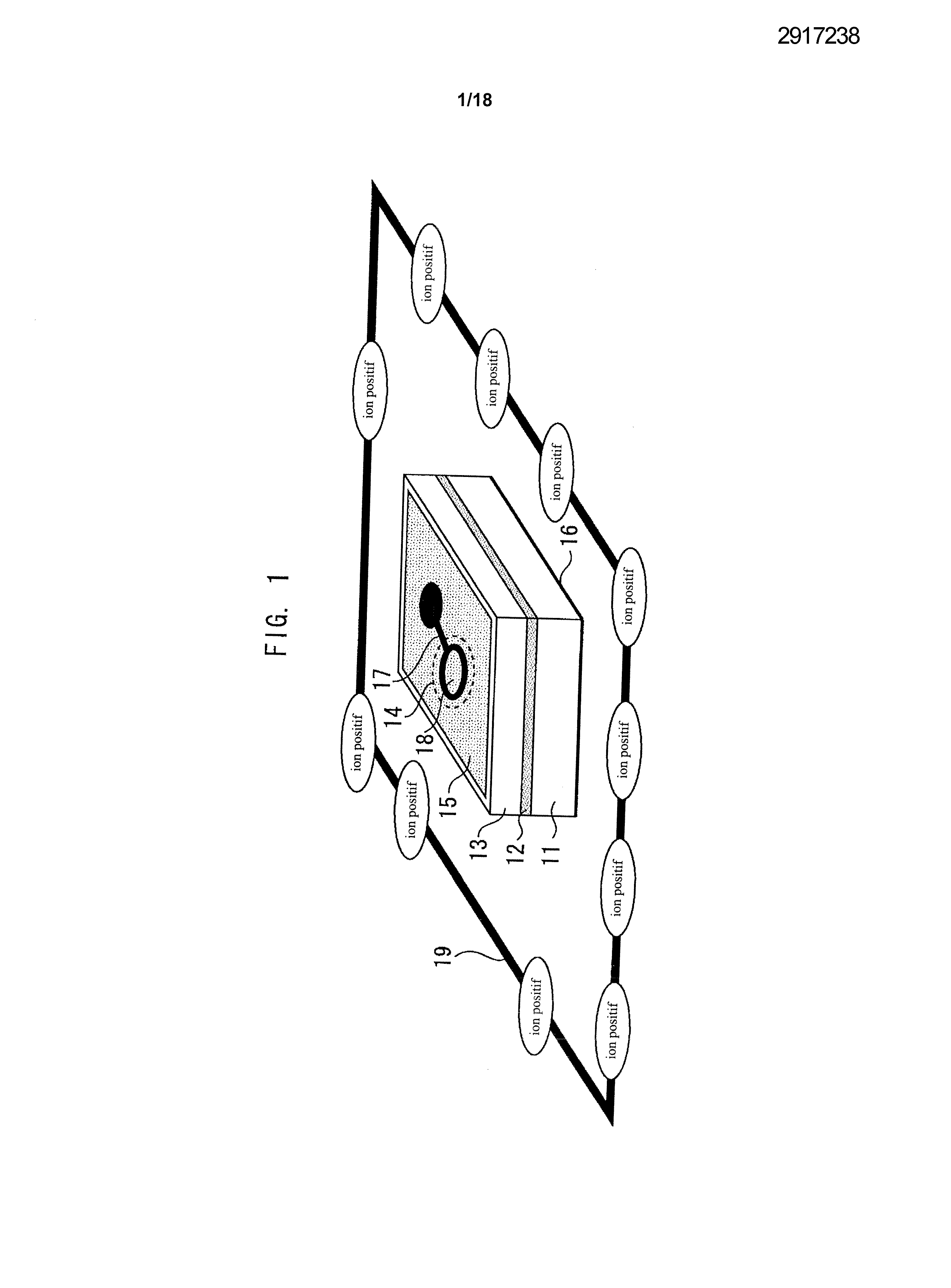
The present invention relates to an optical semiconductor device such as an avalanche photodiode for optical communication and. more particularly, to an optical semiconductor device for improving a property moisture barrier. Figure 18 is a perspective view representing an optical semiconductor device according to the prior art. The optical semiconductor device is an avalanche photodiode for optical communication (refer, for example, the Japanese Patent No. 10-209 486, open to public inspection). 12 A layer pholoabsorbante InGaAs n-type, a layer 13 of InP n-type layer which is a window and a multiplication layer are laminated on one another on a substrate 11 InP n-type. By diffusion of impurities and selective ion implantation, a region 14 InP P-type is formed on a part of the top surface of the layer 13 of InP n-type. The upper surfaces of the layer 13 of InP n-type and of the type of region 14 InP P are covered by a surface protective film 15. A cathode electrode 16 is connected to the underside of the substrate 11 InP n-type. An anode electrode 17 of annular shape is connected to the upper surface of the region 14 P InP The region surrounded by the anode electrode 17 is a light receiving section 18. One will now explain the operation of the semiconductor optical device described above. A voltage less than that of the cathode electrode 16 is applied to the anode electrode 17. Therefore, a reverse bias is applied between the anode electrode 17 and the cathode electrode 16. The reverse bias (operating voltage) is set to be about 90% of a breakdown voltage. Since the breakdown voltage is very high, of the order of 20 to 80 V, the reverse bias reaches a maximum of about 70 V. An optical signal enters the light receiving section 18, from above in Figure 63 InP Since a layer of P-type has a wide bandgap, it allows light to a wavelength (1.3 pm and 1.55 μπΐ) used in optical communication normal pass without absorbing it. The light that has passed is absorbed by the light absorbing layer 12 of n-type InGaAs which has a low energy gap, by producing electrons and holes. These holes pass through a depletion layer, penetrate the stratum 13 of InP n-type which a strong electric field is applied, cause an avalanche multiplication under the effect of such a strong electric field and produce as large number of new electrons and holes. Therefore, an optical signal is extracted from the semiconductor optical device in the form of a signal intensity multiplied. This allows a signal to intensity value more than ten times greater by comparison to the case where the multiplication occurs. Many parts such as a capacitor circuit, a wire, a preamplifier, a resistor, a support are employed about an optical semiconductor device and a housing in the form of a base is also used for mounting the optical semiconductor device. A non-negligible number of charged ions adhere to these elements. These charged ions have a property of ctre attracted to where a voltage is applied. Therefore, positive ions are attracted around the anode electrode 17 to which is applied a negative bias. This causes a leakage current to begin to traverse the surface of the chip. Therefore, a current flows from the anode electrode 17 to the layer 13 of InP n-type. When the semiconductor optical device is employed in a high-humidity atmosphere, a leakage current passes through the top surface of the die with moisture and causes corrosion. This corrosion attacks the surface protective film 15 and causes a further increase of the intensity of the electric current. Therefore, and degraded 101 of the discolored parts appear on the top surface of the die. The decolourisation occurs from the end of the protection film 15 surfaces toward the anode electrode 17. Furthermore, discoloration can also grow to the periphery from the anode electrode 17 as a starting point. Advancement of the bleaching leads finally to a problem in prevention of shorting and openings. Therefore, the optical semiconductor device according to the prior art cannot be used in a high-humidity atmosphere. Furthermore, even if the optical semiconductor device is sealed with a lid or the like, strict measurements are to be taken so that there is no infiltration of moisture into the cover. The present invention was constructed to overcome the above-mentioned problems and the present invention provides a semiconductor optical device which can exhibit improved anti-moisture property. According to one aspect of the present invention, a semiconductor optical device includes: a semiconductor layer of a first conductivity type; a semiconductor region of a second conductivity type formed on line portion of an upper surface of the semiconductor layer of the first conductivity type; a surface protective film which covers the upper surfaces of the semiconductor layer of the first conductivity type and the semiconductor region of the second conductivity type; a first electrode connected to the semiconductor layer of the first conductivity type; a second electrode connected to the semiconductor region of the second conductivity type and to which is applied a voltage lower than that of the first electrode; and a low voltage electrode which is arranged to surround the second electrode and to which is applied a voltage lower than that of the first electrode. It is possible to improve an anti-moisture property. The invention will be better understood with the study of the detailed description of a exemplary embodiment of non-limiting example and illustrated in the accompanying drawings on which: figure 1 is a perspective view representing an optical semiconductor device according to the embodiment of the present invention no. 1; figure 2 illustrates the result of a measurement of the proportion of elements are decolorized and degraded due to a change in the voltage applied to the low voltage electrode; figure 3 is a perspective view representing an optical semiconductor device according to the embodiment of the present invention no. 2; figure 4 is a perspective view representing an optical semiconductor device according to the embodiment of the present invention no. 3; figure 5 is a perspective view representing an optical semiconductor device according to the embodiment of the present invention no. 4; the Ligurian 6 is a plan view representing an optical semiconductor device according to the embodiment of the present invention no. 5; figure 7 is a plan view representing an optical semiconductor device according to the embodiment of the present invention no. 6; figure 8 is a cross-sectional view and a potential distribution of Figure 7; figure 9 is a plan view representing an optical semiconductor device according to the embodiment no. 7 of the present invention; figure 10 is a plan view representing an optical semiconductor device according to the embodiment of the present invention no. 8: figure 11 is a plan view representing an optical semiconductor device according to the embodiment of the present invention no. 9; figure 12 is a plan view representing an optical semiconductor device according to the embodiment of the present invention no. 10; figure 13 is a plan view representing an optical semiconductor device according to the embodiment of the present invention no. 11; figure 14 is a plan view representing an optical semiconductor device according to the embodiment of the present invention no. 12; figure 15 is a plan view representing an optical semiconductor device according to the embodiment of the present invention no. 13; figure 16 is a perspective view representing an optical semiconductor device according to the embodiment of the present invention no. 14; figure 17 is a perspective view representing an optical semiconductor device according to the embodiment of the present invention n 5 ; and figure 18 is a perspective view representing an optical semiconductor device according to the prior art. Form embodiment no. 1 Figure 1 is a perspective view representing an optical semiconductor device according to the embodiment of the present invention no. 1. The optical semiconductor device is an avalanche photodiode for optical communication. A InGaAs light absorbing layer 12 n-type and a layer 13 of InP n-type (semiconductor layer of the first conductivity type) which is a layer window and a multiplication layer are laminated on one another on a substrate 11 InP n-type. By diffusion of impurities and selective ion implantation, a region 14 InP P-type (semiconductor region of the second conductivity type) is formed on a part of the top surface of the layer 13 InP n-type. The upper surfaces of the layer 13 in InP and of the n-type region 14 InP P-type are covered by a surface protective film 15. A cathode electrode 16 (first electrode) is connected to the underside of the substrate 11 InP n-type. An anode electrode 17 annular (second electrode) is connected to the upper surface of the region 14 P InP The region surrounded by the anode electrode 17 is a light receiving section 18. A voltage less than that of the cathode electrode 16 is applied to the anode electrode 17. In the present embodiment, a low voltage electrode 19 is arranged surrounding the anode electrode 17. A voltage less than that of the cathode electrode 16 is applied to the low voltage electrode 19. This causes positive ions present around the semiconductor optical device to be trapped by the low voltage electrode 19 and prevents positive ions does gather around the anode electrode 17. Therefore, discoloration and degradation are less likely to occur and the moisture barrier property can be improved. Figure 2 illustrates the result of a measurement of the proportion of elements are decolorized and degraded under the effect of a change in the voltage applied to the low voltage electrode. Experience took place under conditions where the temperature was set at 85 °C, moisture to 85% and 90% of a voltage breakdown voltage has been applied between the anode electrode 17 and the cathode electrode 16. Following the experience, 100% of the elements are decolorized and degraded in the case (a) in which no voltage has been applied to the low voltage electrode 19 and in the case (c) wherein a voltage greater than that of the cathode electrode 16 has been applied. In contrast, in the case (b) wherein a voltage lower than the cathode electrode 16 has been applied to the low voltage electrode 19, 0% of the elements are decolorized and degraded. The result of this experience, it has been confirmed that this embodiment can prevent discoloration and degradation. On Figure 1, the entire periphery of the chip of the semiconductor optical device is surrounded by the low voltage electrode 19, but a similar effect can also be provided without necessarily surround all the peripheries. Furthermore, a similar effect may also be obtained by surrounding the periphery of the anode electrode 17 with the low voltage electrode 19 without surrounding the entire chip. Form embodiment no. 2 Figure 3 is a perspective view representing an optical semiconductor device according to the embodiment of the present invention no. 2. Die semiconductor optical device similar to that of the embodiment 1 is mounted on a ri insulating base 21. An electrode 22 on the side of the base 21 makes contact with a cathode electrode 16 of the semiconductor optical device. A low voltage electrode 19 is disposed on the base 21 so as to surround the electrode 22 on the side of the base. An anode electrode 17, the electrode 22 on the side of the base, the low voltage electrode 19 are electrically connected to an external circuit (not shown) respectively via wires 23, 24, 25. A voltage less than eelle of the electrode 22 on the side of the base is applied to the low voltage electrode 19. This causes positive ions on and around the base 21 to be attracted to the low voltage electrode 19, and therefore a smaller number of positive ions are attracted to the anode electrode 17. Therefore, discoloration and degradation are less likely to occur and the anti-moisture property of the device can be improved. On Figure 3, the entire periphery of the electrode 22 on the side of the base is surrounded by the low voltage electrode 19, but a similar effect can also be provided without necessarily surround the entire periphery. Form embodiment no. 3 Figure 4 is a perspective view representing an optical semiconductor device according to the embodiment of the present invention no. 3. An anode electrode 17 and a low voltage electrode 19 are electrically connected by a wire 23. For the rest, the same configuration as the embodiment n 2. This eliminates the need of a power supply to make the voltage of the low voltage electrode 19 lower than the voltage of a cathode electrode 16. Form embodiment no. 4 Figure 5 is a perspective view representing an optical semiconductor device according to the embodiment of the present invention no. 4. A section high impedance 26 is mounted between an anode electrode 17 and a low voltage electrode 19. This section high impedance 26 consists of a thin film resistor, a chip resistance, an induction coil, induction coil chip or the like and the impedance thereof is equal to or greater than 20 O. However, the impedance of the high impedance section 26 is preferably greater than or equal to 200 to 300 Form embodiment no. 5 Figure 6 is a plan view representing an optical semiconductor device according to the embodiment of the present invention no. 5. A low voltage electrode 19 is formed on a surface protective film 15 in the form of a thin metal film of Ti, Cr, Au or other. Pad 31 is connected to the low voltage electrode 19 and a wire 32 is connected to the pad 31. A voltage less than that of the cathode electrode 16 is applied to the low voltage electrode 19 via the bonding pad 31 and 32 of the wire. For the rest, the same configuration as the embodiment no. 1. This allows the low voltage electrode 19 attracts positive ions on the upper surlace the chip and for longer serves to prevent degradation, even in an atmosphere containing moisture. The low voltage electrode 19 can also be formed under the surface protective film 15. In this case, some or all of the protective film 15 of surfaces on the low voltage electrode 19 can be eliminated to make the low voltage electrode 19 is exposed. Furthermore, the low voltage electrode 19 may also not be made of metal, but by providing a diffusion region with P type dopant implanted in the surface of a layer 13 InP n-type. Furthermore, in Figure 6, the entire circumference of the anode electrode 17 is surrounded by the low voltage electrode 19, but a similar effect can also be provided without necessarily surround the entire periphery. Form embodiment no. 6 Figure 7 is a plan view representing a optical device semicondueteur no. 6 according to the embodiment of the present invention. A high voltage electrode 33 is disposed between a low voltage electrode 19 and an anode electrode 17 so as to surround the anode electrode 17. The high voltage electrode 33 is formed on a surface protective film 15 in the form of a thin metal film of Ti, Cr, Au or other. Pad 34 is connected to the high voltage electrode 33 and a wire 35 is connected to the pad 34. A voltage higher than those of the anode electrode 17 and 19 of the low voltage electrode is applied to the high voltage electrode 33 via the bonding pad 34 and wire 35. For the rest, the same configuration as the embodiment no. 5. Figure 8 is a cross-sectional view and a potential distribution of Figure 7. As shown on Fig., in assume a potential M-shaped causes the formation of a potential barrier around the anode electrode 17 at the center, thereby preventing positive ions approach of the anode electrode 17. This serves to prevent for longer degradation, even in an atmosphere containing moisture. Despite the absence of the high voltage electrode 33 in the embodiment no. 5, the surface protective film 15 is in contact with the layer 13 InP n-type, thereby increasing the potential of the portion corresponding to the high voltage electrode 33 and produces a similar effect. Form embodiment no. 7 Figure 9 is a plan view representing an optical semiconductor device according to the embodiment no. 7 of the present invention. The edges of a surface protective film 15 are covered by a metal film 36. For the rest, the same configuration as the embodiment no. 6. By covering the boundary between the edges of the film 15 and the surface protective layer 13 InP n-type with the metal film 36, it is possible to prevent moisture and the charged ions to permeate under the surface protective film 15. Therefore, it is possible to prevent the progression of the discoloration and degradation from the sides of the surface protective film 15. Form embodiment no. 8 Figure 10 is a plan view representing an optical semiconductor device according to the embodiment of the present invention no. 8. A surface protective film 15 is provided with an opening 37 between a low voltage electrode 19 and an anode electrode 17 so as to surround the anode electrode 17. Through this opening 37 is uncovered a layer 13 InP n-type, the voltage of which is higher than that of the low voltage electrode 19. For the rest, the same configuration as the embodiment no. 5. The presence of the opening 37 prevents the positive ions approach the anode electrode 17 as in the case of the embodiment no. 6. The formation of a thin metal film to cover the opening 37 can prevent infiltration of moisture and of charged ions under the surface protective film 15. Form embodiment no. 9 Figure 11 is a plan view representing an optical semiconductor device according to embodiment no. 9 of the present invention. A region 41 P-type diffusion is formed on the surface of a layer 13 InP n-type, and this region 41 P-type diffusion is electrically connected to a 14 InP type P. A surface protective film 15 is partially suppressed electrodes and contacts 42, 43 are formed. A low voltage electrode 19 is electrically connected to the P-type region InP through the electrode contact region 41 and 42 of the-type diffusion P. An high voltage electrode 33 is electrically connected to the layer 13 InP n-type via the contact electrode 43. This configuration eliminates the need to provide, from the outside, power to the low voltage electrode 19 and to the high voltage electrode 33. Performing-type diffusion region 41 P thinner or shallower to have a larger resistance is effective to prevent a high frequency signal produced by a light receiving section 18 from escaping to the low voltage electrode 19. Furthermore, instead of using the electrodes of eontacts 42, 43, it is also possible to connect the entire low voltage electrode 19 and the high voltage electrode 33 respectively to the region 41 P-type diffusion layer and the 13 InP n-type. Form embodiment no. 10 Figure 12 is a plan view representing an optical semiconductor device according to the embodiment of the present invention no. 10. A groove 44 is formed on the surface of a layer 13 InP n-type, between a low voltage electrode 19 and an anode electrode 17, so as to surround the anode electrode 17. A metal film 45 for covering the groove 44 is formed on a surface protective film 15. For the rest, the same configuration as the embodiment n 5. The groove 44 may provide insulation between a light receiving section 18 and the end of the chip. However, the groove 44 present on the surface of the puee is easily subject to constraints, these constraints and damage the film 15 for protecting surfaces of which cause discoloration and degradation from the groove 44. Therefore, by covering the groove 44 with the metal film 45, it is possible to prevent moisture and the charged ions to permeate under the surface protective film 15. Form embodiment no. 11 Figure 13 is a plan view representing an optical semiconductor device according to the embodiment of the present invention no. 11. A surface protective film 15 is partially suppressed electrodes and contacts 46, 47 are formed. A low voltage electrode 19 is electrically connected to a diffusion 49 F type within a groove 44 via the contact electrode 46 and a wiring 48. A metal film 45 is electrically connected to a layer 13 in InP n-type out of the groove 44 through the electrode contact 47. For the rest, the same configuration as the embodiment no. 10. Therefore, a voltage lower than the cathode electrode 16 is applied to the low voltage electrode 19. Furthermore, a voltage greater than that of the low voltage electrode 19 is applied to the metal film 45. Therefore, there is no need to provide, from the outside, power to the low voltage electrode 19 and the metal film 45. The region 49 P-type diffusion is not necessarily present. Therefore, the low voltage electrode 19 may be electrically connected to a layer 13 in InP n-type within the groove 44 through the electrode contact 46 and 48 of the wiring. Indeed, the layer 13 InP n-type within the groove 44 has a lower voltage than the layer 13 in InP n-type out of the groove. However, a lower voltage can be obtained with the presence of the-type diffusion region 49 P. Also, the region 49 P-type diffusion can be connected to a region 14 in InP P-type of a light receiving section 18. In this case, making a thinner or shallower junction between the region 49 P-type diffusion region 14 InP and the P-type to have a larger resistance is effective to prevent a high frequency signal produced in the light receiving section 18 from escaping toward the low voltage electrode 19. Form embodiment no. 12 Figure 14 is a side-view showing an optical semiconductor device according to the embodiment of the present invention no. 12. A chip 53 of the optical semiconductor device is mounted on a rod 51 through a insulating base 52. Other components forming chips 54 . 55 are also mounted on the rod 51. The chips are electrically connected with one another by a wire 56. Terminals for leads project from 57 of the rod 51. Electricity is supplied to the shaft 51 so that the voltage thereof is lower than that of the cathode electrode of the semiconductor optical device. Therefore, the positive ions present on the rod 51 are attracted to the rod 51 and the positive ions attracted to the anode electrode of the semiconductor optical device are therefore fewer. Therefore, discoloration and degradation are less likely to occur and thus it is possible to improve the anti-moisture property. Form embodiment no. 13 Figure 15 is a side-view showing an optical semiconductor device according to the embodiment of the present invention no. 13. A insulating base 58 whose upper surface is covered by a metal as the electrode is disposed between a shaft 51 and a base 52. Electricity is supplied to the top surface of the base 58 so as to have a voltage lower than that of a cathode electrode of the semiconductor optical device. For the rest, the same configuration as the embodiment no. 12. Therefore, the positive ions present on the rod 51 are attracted to the base 58 and the positive ions attracted to the anode electrode of the semiconductor optical device are therefore fewer. Therefore, discoloration and degradation are less likely to occur and thus it is possible to improve the anti-moisture property. Form embodiment no. 14 Figure 16 is a perspective view representing an optical semiconductor device according to the embodiment of the present invention n 14. The optical semiconductor device is a laser diode of the type that emits light through an end face. A activated layer 61 is formed in a layer 13 InP n-type (couehc semiconductor of a first conductivity type). By diffusion of impurities and selective ion implantation, a region 14 InP P-type (semiconductor region of a second conductivity type) is formed in a part of the top surface of a layer 13 InP n-type. The upper surfaces of the layer 13 InP and of the n-type region 14 InP P-type are covered by a surface protective film 15. A éleetrode cathode 16 (first electrode) is connected to the lower side of the layer 13 InP n-type. An anode electrode (second electrode) 17 is connected to the upper surface of the region 14 InP type P. An voltage greater than that of the cathode electrode 16 is applied to the anode electrode 17. In the present embodiment, a high voltage electrode 62 is arranged to surround an anode electrode 17. A voltage greater than that of the cathode electrode 16 is applied to the high voltage electrode 62. This causes the negative ions present around the semiconductor optical device to be trapped by the high voltage electrode 62 and, thereby, prevents negative ions does gather around the anode electrode 17. Therefore, discoloration and degradation are less likely to occur and thus it is possible to improve the anti-moisture property. The above-described configuration can be combined with the configurations of the embodiments 2 to 13. Form embodiment no. 15 Figure 17 is a perspective view representing an optical semiconductor device according to the embodiment of the present invention no. 15. The optical semiconductor device is a laser diode of the light emission type by an end face. A activated layer 61 is formed in a layer 63 InP P-type (semiconductor layer of a first conductivity type). By diffusion of impurities and selective ion implantation, a region 64 InP n-type (semiconductor region of a second type of conduetivité) is formed in a part of the top surface of the layer 63 InP type P. The upper surfaces of the layer 63 InP and of the P-type region 64 InP n-type are covered by a surface protective film 15. An anode electrode 65 (first electrode) is connected to the lower side of the layer 63 InP type P. An cathode electrode 66 (second electrode) is connected to the upper surface of the region 64 InP n-type. A voltage lower than the anode electrode 65 is applied to the cathode electrode 66. In the present embodiment, a low voltage electrode 19 is arranged so as to surround the cathode electrode 66. A voltage lower than the anode electrode 65 is applied to the low voltage electrode 19. This causes the positive ions present around the semiconductor optical device to be trapped by the low voltage electrode 19 and, thereby, prevents positive ions does gather around the cathode electrode 66. Therefore, discoloration and degradation are less likely to occur and, thereby, it is possible to improve the anti-moisture property, The configuration described above can be combined with the configurations of the embodiments 2 to 13. An n-type InGaAs light absorbing layer and an n-type InP layer (first conductivity type semiconductor layer), which is a window layer, and a multiplication layer are multilayered one atop another on an n-type InP substrate. By selectively diffusing impurities and implanting ions, a p-type InP region second conductivity type semiconductor region) is formed on a part of the top surface of the n-type InP layer. The top surfaces of the n-type InP layer and p-type InP region are covered with a surface protection film. A cathode electrode (first electrode) is connected to the underside of the n-type InP substrate. A ring-shaped anode electrode (second electrode) is connected to the top surface of the p-type InP region. A low-voltage electrode surrounds the anode electrode. A voltage lower than that of the cathode electrode his applied to this low-voltage electrode. 1. An optical semiconductor device, characterized in that it comprises: a semiconductor layer (13) of a first conductivity type; a region (14) semiconductor of a second conductivity type, formed on a portion of an upper surface of the semiconductor layer (13) of the first conductivity type; a film (15) of which covers the upper surfaces of the semiconductor layer (13) of the first type of conductivity and the semiconductor region (14) of the second conductivity type; a first electrode (16) connected to the semiconductor layer (13) of the first conductivity type; a second electrode (17) which is connected to the semiconductor region (14) of the second conductivity type and to which is applied a voltage lower than that of the first electrode (16); and a low voltage electrode (19) which is arranged so as to surround the second electrode (17) and to which is applied a voltage lower than that of the first electrode (16). 2. An optical semiconductor device according to claim 1, characterized in that the low voltage electrode (19) is electrically connected to the second electrode (17). 3. An optical semiconductor device according to claim 2, characterized in that it further comprises a high impedance section (26) mounted between the ' clcctrode low voltage (19) and the second electrode (17), and having an impedance equal to or greater than 20 Ω. 4. An optical semiconductor device according to claim 1, characterized in that it further comprises a high voltage electrode (33) disposed between the low voltage electrode (19) and the second electrode (17) so as to surround the second electrode (17) and to which is applied a voltage higher than those of the other electrode (17) and the low voltage electrode (19). 5. An optical semiconductor device according to claim 1, characterized in that it further comprises a metal film (36) which covers the edges of the film (15) surface protection. 6. An optical semiconductor device according to claim 1, characterized in that the film (15) surface protection is provided with an opening (37) between the low voltage electrode (19) and the second éleetrode (17) so as to surround the second electrode (17), and the layer (13) the first conducting type semiconductor is exposed through the opening (37). 7. An optical semiconductor device according to claim 1, characterized in that the low voltage electrode (19) is electrically connected to the semiconductor region (14) of the second conductivity type. 8. An optical semiconductor device according to claim 4, characterized in that the high voltage electrode (33) is electrically connected to the semiconductor layer (13) of the first conductivity type. 9. An optical semiconductor device according to claim 1, characterized in that it further comprises: a groove (44) formed in the surface of the semiconductor layer (13) of the first conductivity type between the low voltage electrode (19) and the second electrode (17) so as to surround the second electrode (17); and a metal film (45) formed on the eom (15) surface protection to cover the groove (44). 10. An optical semiconductor device according to claim 9. characterized in that the low voltage electrode (19) is electrically connected to the semiconductor layer (13) of the first conductivity type or the semiconductor region (14) of the second conductivity type within the groove (44). 11. An optical semiconductor device according to claim 9, characterized in that the metal film (15) is electrically connected, out of the groove (44), (13) to the semiconductor layer of the first conductivity type. 12. An optical semiconductor device, characterized in that it comprises: a semiconductor layer (13) of a first conductivity type; a region (14) semiconductor of a second conductivity type, formed on a portion of an upper surface of the semiconductor layer (13) of the first conductivity type; a film (15) of which covers the upper surfaces of the semiconductor couehe (13) of the first type of conductivity and the semiconductor region (14) of the second conductivity type; a first electrode (16) connected to the semiconductor layer (13) of the first conductivity type; a second electrode (17) which is connected to the semiconductor region (14) of the second conductivity type and to which is applied a voltage lower than that of the first electrode (16); and a high voltage electrode (33) which is arranged so as to surround the second electrode (17) and to which is applied a voltage lower than that of the first electrode (16). SEMICONDUCTOR OPTICAL DEVICE