SEMICONDUCTOR DEVICE
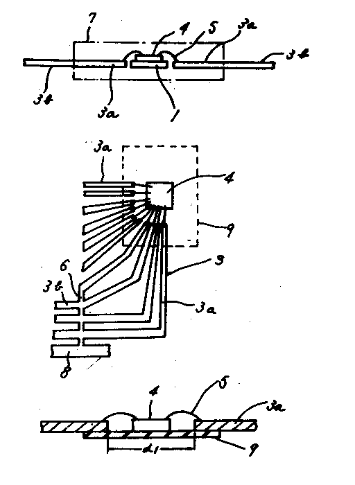
PURPOSE: To prevent defective wire bonding due to the instability of an inner lead and defective short circuits, etc. by a wire by sealing a metallic small wire connected between the electrode of a pellet and a lead, the pellet and the inner end of the lead with a resin molding body so as to be surrounded. CONSTITUTION: The semiconductor device uses a lead frame consisting of only a plurality of the leads 3 with no tab and tab hanging lead, a dam 6 connecting the leads and a peripheral frame 8, and has the pellet 4, to which a semiconductor element is formed, and an insulating sheet piece 9 simultaneously supporting and fixing the inside sections of a plurality of the leads 3 surrounding the pellet, the inner leads 3a, on one plane, and the electrode of the pellet 4 and the inner leads 3a are connected by the wires 5 while the pellet and one parts of the leads are sealed with the resin molding body 7. Since the inner leads are fixed by a resin tape, they are not moved vertically even when they are long, empty touch in case of bonding can be prevented, and defective bonding can be removed. COPYRIGHT: (C)1983,JPO&Japio