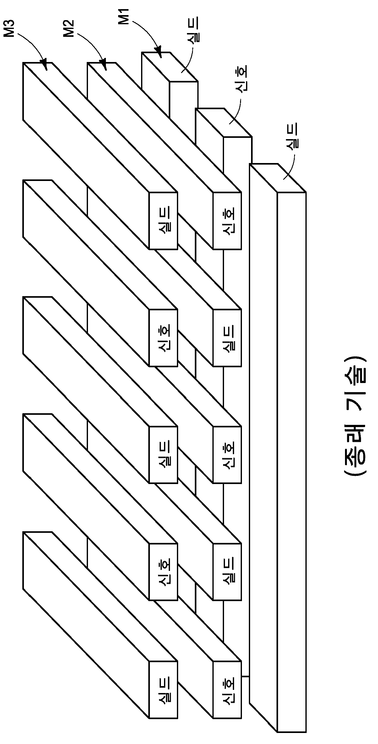
하측 배선 레벨의 실드 라인에 전기적으로 결합된 상측 배선 레벨의 실드 라인을 갖는 어셈블리
Wiring level of shield line is electrically coupled with the upper wiring level of shield line assembly. The integrated circuit includes a multi-level stack can be wiring. Level includes a shield line can be arranged in alternating signal line. Shield line between adjacent signal line can be used for mitigating cross - torque. 3 Example configuration including two of stacked wiring level 1 also to is also shown. Specifically, the configuration number 1 level interconnect (M1), (M2) connection number 2, number 3 which show connection (M3); M1 M2 M3 is on which is on disclosed. 3 But of wiring levels are shown, under and/or other wiring level above the level shown level shown in accomplishing understanding may be negative. In addition, wiring level shown labeled M1 - M3, if there is other wiring level, shown as level number according to a number of wiring levels shown below seal has the wiring levels present, M2 - M4; M3 - M6; etc. disclosed. Level shown arranged in alternate with each shield line comprises a signal line. In shield line level at another level in the shield line electrically connected to said level above and below can be preferably. For example, level (M1) (M2) (M3) in shield line level in shield line and level in shield line electrically connected is it can mitigate coupling noise between vertically stacked levels can be advantageous. Level (M1) (M2) in line level in line (M1) (M2) extending perpendicular to the level line connection of the shield line relatively close to a leveling agent from 2000. However, level (M3) (M2) (M2) from a level line connection of the wiring level (M3) in shield line level in wiring extending in parallel with a level (M2) and (M3) is staggered with respect to the shield line level because door number is under or over. The, level (M2) (M3) vertical overlap is free shield line between shield line level. In Figure 1 level (M2, M3) shown as types of stack level of shield lines enabling coupling between development architecture will preferably. Figure 1 shows a prior art arranged to synthesize 3 dimensional wiring levels also are disclosed. In the embodiment shown is also 2 - 2c also wiring levels exemplary arrangement are disclosed. Figure 2 shows a plane are disclosed. Also 2a - 2c of Figure 2 also is used in line 2A - 2A, 2B - 2B and 2C - 2C cross-sectional drawing along are disclosed. Figure 3 shows a region "3" of the field of view of Figure 2 also are disclosed. In the embodiment shown is also 4 and also 4a wiring levels exemplary arrangement are disclosed. Figure 4 shows a plane are disclosed. Of Figure 4 taken along line 4A - 4A cross-sectional drawing 4a is also are disclosed. Figure 5 shows a decomposition of an exemplary assembly of wiring levels also in the embodiment are disclosed. Of Figure 5 drawing in of level 3 are stacked disclosed. 6 - Figure 8 shows a plane view of Figure 5 of discrete level also are disclosed. Figure 9 shows a 3 level of interconnected receiving shield line of an exemplary mesh plane view of Figure 5 as shown are disclosed. Figure 10 shows a wiring levels also another aspect of decomposition of assembly in the embodiment are disclosed. Of Figure 10 drawing of level 3 are stacked in the cup. 11 - Figure 13 shows a plane view of Figure 10 of discrete level also are disclosed. Figure 14 shows a 3 receiving an exemplary mesh shield line of level of interconnected as shown in plane view of Figure 10 are disclosed. Over the substrate plane view and also blocks assembly 15a, 15b also includes alternating signal line shield line 15a also turned to show shown extended region are disclosed. Of wiring layer are stacked and also in plane view of 15a of Figure 5 3, also shown in part may also be in the area of 5 15a of "also 5". Plane view of an exemplary array over the substrate 16a also are disclosed. A ring-shaped line (redundant) alternating signal line 16b is also shown (or dummy (dummy)) structure for redundant and shown to an enlarged area 16a shown also are disclosed. Figure 17 shows a stacked wiring layer 2 of an exemplary array plane from circuit also are disclosed. Also shown in Figure 18 shows a stacked wiring layers of alternating signal line and shielded line redundant (or dummy) structure of Figure 17 and turned to show an enlarged region timing are disclosed. Figure 19 shows a comparing plane also exemplary circuit arrangement are disclosed. Figure 20 shows a pair of exemplary circuit configuration also comparing the plane are disclosed. Figure 21 shows a circuit arrangement of Figure 20 also can be used in one of the decomposition of an exemplary assembly of wiring layer are disclosed. Of Figure 21 drawing of the wiring layer on the 3 are stacked disclosed. The individual wiring layer 22 - Figure 24 shows a plane view of Figure 21 also are disclosed. Figure 25 shows a 23 and 24 along line 25 - 25 are also shown also, 23 (M2, M3) of Figure 24 and also passed through the wiring layer on a side end face are disclosed. Figure 26 shows a extended region of Figure 24 and 23 which also also shown, when wiring layer stacked on a copper interconnection of Figure 23 decodes of Figure 24. Also 23 and 24 to the dashed lines "also 26" of Figure 26 region is also exhibits. 27A - 27c also relates to a method for examples of alternative configuration of Figure 23 M2 wiring layers is also related to an enlarged plane view are disclosed. Figure 28 shows a circuit arrangement can be used in one of the decomposition of an exemplary wiring layer assembly of Figure 20 also are disclosed. In as an error of Figure 28 drawing 3 are stacked disclosed. Individual layers of 29 - Figure 31 shows a plane view of Figure 28 also are disclosed. 32A - 32c of Figure 31 and 30 also is also also line 32A - 32A, 32B - 32B and 32C - 32C along, (M2, M3) of Figure 31 and passed through the side cross-sectional drawing wiring layer 30 also are disclosed. Figure 34 shows a wiring layer (M3) of Figure 31 and 33 also alternative configuration shown for example also for the enlargement area of plane are disclosed. Figure 36 shows a alternative configuration shown wiring layer (M2) example of Figure 30 also 35 and also for the enlargement area of plane are disclosed. In the embodiment of signal line and shielded line metal line layer portion configured to be offset region comprising architecture. The upper wiring layer wiring layer shield line between shield line such an offset region, although these interconnections of shield line even mutually substantially parallel wiring layer shield line in one arrangement of Figure 1 and similar to the upper wiring layer shield line staggered [toy compared to even, vertical overlap causes may occur. In the embodiment described with reference to exemplary also includes 2 - 36. The reference also 2 - 2c also, integrated assembly (510) is a region of the shown disclosed. Assembly (510) comprises (M2, M3) is vertically stacked pair of wiring level. Level (M2) (M3) to indicate such level below the level of Figure 2 plane view in dashed lines shown substrate. Level (M3) includes a shield line (512) and shielded line directly adjacent to the signal line (514) comprises. Line (512, 514) wiring level (M3) in alternating relationship can exhibit a plurality of shield line and signal line. Level (M2) includes a shield line (516) and shielded line directly adjacent to the signal line (518) comprises. Wiring (516, 518) wiring level (M2) in alternating relationship can exhibit a plurality of shield line and signal line. In some in the embodiment, the wiring levels (M3) can be referred to as level wiring number 1, number 2 below the wiring levels (M2) can be referred to as the wiring levels number 1 at an interconnect level. In shield line wiring levels number 1 (512) and signal line (514) can be referred to as the shield line and number 1 signal line number 1, this number 1 number 1 number 1 shield line and a plurality of alternating arrangement wiring levels over signal line can exhibit. Similarly, in shield line wiring levels number 2 (516) and signal line (518) can be referred to as the shield line and number 2 signal line number 2, this shield line and a plurality of number 2 number 2 number 2 alternating arrangement wiring levels over signal line can exhibit. Number 1 shield line (512) is number 1 segment (520) offset laterally from segment number 1 and number 2 segment (522) has. Segment number 1 (520) and number 2 segment (522) is link segment (524) communicate with one another through connected thereto. Link segment (524) is number 1 segment (520) end of segment number 2 (522) ends can be arranged. Segment number 1 (520) is link segment (524) from the end of said long be. Segment number 2 (522) is link segment (524) from the other end of segment number 1 (520) can be opposite to the long. Similarly, signal line number 1 (514) is number 1 segment (526), offset laterally from segment number 1 number 2 segment (528), and number 1 and number 2 segment (526, 528) interconnecting link segment each other (530) having a predetermined wavelength. Link segment (530) is number 1 segment (526) end of segment number 2 (528) ends can be arranged. Segment number 1 (526) is link segment (530) can be elongated from one end. Segment number 2 (528) includes a link segment (530) from the other end of segment number 1 (526) opposite to the long be. Wiring levels number 2 (M2) (M3) number 1 number 2 signal line is number 2 in shield line and similar segments at an interconnect level. However, to simplify the description, shield line number 1 number 2 number 2 signal line segment of the shield line (512) and number 1 signal line (514) of number 1 and number 2 number 3 and number 4 for discrimination segment will referred to as segments. The, shield line number 2 (516) is number 3 segments (532) offset laterally from segment number 3 and number 4 segments (534) has. Segment number 3 (532) and number 4 segments (534) is link segment (536) communicate with one another through connected thereto. Link segment (536) is number 3 segments (532) end of segment number 4 (534) ends can be arranged. Segment number 3 (532) is link segment (536) can be elongated from one end. Segment number 4 (534) is link segment (536) from the other end of segment number 3 (532) opposite to the long be. Similarly, signal line number 2 (518) is number 3 segments (538), number 4 segment offset laterally from segment number 3 (540), and number 3 and number 4 segments (538, 540) interconnecting link segment each other (542) has. Link segment (542) is number 3 segments (538) end of segment number 4 (540) can be arranged for connecting an end of. Segment number 3 (538) is link segment (542) can be elongated from one end. Segment number 4 (540) is link segment (542) from the other end of segment number 3 (538) opposite to the long be. In some in the embodiment, number 1 (M3) in link segment at an interconnect level (524, 530) can be referred to as link segment is number 1, number 2 (M2) at an interconnect level in link segment (536, 542) is segments are links in different wiring level can be distinguished to number 2 can be referred to as link segment. The shaft system of Figure 2 plane view number encoded adjacent ball. The shaft axle system number 1 (503) axis extending orthogonal to the axis of the number 1 and number 2 (505) are shown as follows. Number 1 and number 2 segment (520, 522, 526, 528) is principally axis (503) is extended along a direction corresponding to the number 1, link segment (524, 530) is principally shaft (505) extended in a first direction corresponding to the number 2. Segment "segment is way non-(wavy) to even if heat is applied even along the entire course is segment display direction indicate" mainly (primarily)" extending along the display direction is displayed. In some in the embodiment, segment may be substantially straight, that the term "substantially straight" in straight segment number within tolerance measurement bath and rational means other. Number 3 and number 4 segments (532, 534, 538, 540) is in addition axis (503) extending mainly corresponding to number 1 direction, link segment (536, 542) is shown in the embodiment mainly in number 2 shaft (505) extends along the substrate. In the embodiment shown in, link segment (524) shields line (512) of number 1 and number 2 segment (520, 522) substantially orthogonal to the extending, link segment (530) is signal line (514) of number 1 and number 2 segment (526, 528) substantially orthogonal to the extending, link segment (536) is shield line number 2 (516) number 3 and number 4 of segment (532, 534) extending substantially orthogonal to the, link segment (542) includes a shield line number 2 (518) of segments (538, 540) extending substantially orthogonal to the. ". ". "". The term "substantially orthogonal to the" link segment is an alternative representation segment number bath and rationally within measurement tolerances means that extends orthogonal to the substrate. In other in the embodiment, one or both of link segment such link segment interconnected by segment angle other than perpendicular to the main direction can be. Advantages of the architecture of Figure 2, the offset (i.e., bend) signal line and shielded line presents a number, from shield line (M2) (M3) is a region of the upper wiring level wiring level possible from shield line enables vertically superimposed region are disclosed. Specifically, the upper wiring level of shield line (512) is shown in the overlapping region (544) wiring level in shield line (516) to an area of the vertically superimposed; shield line number 2 (516) shown in segments of number 4 (534) is number 1 shield line (512) of number 1 segment (520) extending below the substrate. Shield line (516, 512) for coupling each other in the overlapping region (544) connected in vertical interconnects (546) ball number is encoded. Vertical interconnects connected (546) interconnecting the line (512) of Figure 2 plane view been shown in dashed lines to indicate underlying (phantom). Vertical interconnection can be extending substantially vertically, the terms "substantially vertical" is interconnected within measurement tolerances perpendicular number bath and rational meaning that the other. In the embodiment shown is overlapped region (544) 2 vertical interconnections shown in 2000. In other in the embodiment, the number in the overlapping region within the overlapping region within which ball 2 presents a number or may be only a single interconnected to at least one of interconnected ball number may be disclosed. In addition, interconnected (546) of Figure 2 plane view along the square but, in other in the embodiment, interconnection is e.g. rectangular, circular, elliptical, and the like may have other shape. Also also 2 - 2c assembly (510) alternative description is as follows. Number 1 in the upper wiring level shield line (512) has an axis (503) that extends in the direction of part number 1 number 1 (548), number 2 direction (for example, shaft (505) direction) portion extending number 2 (550), number 1 and number 3 portion extending in the direction (552) with can be deemed. Part number 2 (550) is part number 1 (548) number 3 a portion (552) interconnecting substrate. Number 1 in the upper wiring layer signal line (514) which is directly adjacent to the shield line number 1, number 4 portion (554), part number 5 (556) and number 6 portion (558) has. Number 4, number 5 and number 6 portion (554, 556, 558) each number 3, part number 1 and number 2 (552, 550, 548) substantially parallel to the up. ". ". "". The term "substantially parallel" rational number bath and measurement in parallel by big within tolerance. Assembly (510) continue the alternative description, in shield line wiring level number 2 (516) is part number 7 (560) and number 8 portion (562) to including a; part number 7 (560) is number 1 shield line (512) portion of number 3 (552) which are aligned substantially perpendicular to the, part number 8 (562) is number 1 signal line (514) portion of number 4 (554) substantially vertically aligned with each other. Shield line number 2 (516) portion is in addition number 7 (560) portion a number 8 (562) the interconnecting part number 9 (564) comprises. Part number 7 (560) is number 1 shield line (512) portion of number 3 (552) under number 1 signal line (514) portion of number 6 (558) extends continuously below; part number 7 (560) is number 1 shield line (512) portion of number 3 (552) substantially vertically aligned with each other. Assembly (510) alternative more continue the description, in the overlapping region (544) is number 1 shield line (512) portion of number 3 (552) and shield line number 2 (516) portion of number 7 (560) and extend over the, connected vertical interconnects (546) is part number 3 (552) portion a number 7 (560) electrically connected to each other. Figure 3 shows a assembly (510) of "3" of the field of view of Figure 2 and also, this assembly within the relationship be used to account for part are disclosed. Shield line (512) in the upper and lower wiring level representing a plurality of shield lines can be considered individual number 1 shield line, signal line (514) in the upper and lower wiring level representing a plurality of signal line can be considered individual number 1 signal line. Similarly, shield line number 2 (516) is a plurality of number 2 shield line wiring level can be considered shield line representing individual number 2, number 2 signal line (518) is representative of a plurality of number 2 individual number 2 signal wiring level can be considered. Number 1 signal line (514) is number 1 shield line (512) which immediately adjacent, the term "directly adjacent" upper wiring level in signal line (514) includes a ring-shaped line (512) between the other signal line less than a threshold (i.e., signal line (514) is the upper wiring level in shield line (512) nearest to the signal line thereby) exhibits. Number 1 shield line (512) is number 1 shield line number 1 segment (520), shield line number 1 number 2 segment (522), and segment number 1 (520) on number 2 segment (522) between link segment (524) has. Link segment (524) can be referred to as link segment includes a shield line number 1. Signal line (514) is number 1 signal line number 1 segment (526), signal line number 1 number 2 segment (528), and number 1 and number 2 segment (526, 528) between link segment (530) having a predetermined wavelength. Link segment (530) is number 1 signal line can be referred to as link segment. Number 1 shield line link segment (524) is number 1 distance (D1 ) By axis (503) of number 1 number 1 along signal line link segment (530) offset from. Shield line number 2 (516) is number 1 signal line number 1 segment (526) number 3 below the area of segment (532) without using a tool. Shield line number 2 (516) is, in addition signal line number 2 segment (528) substrate region of shield line number 1 segment which extends in addition number 1 (520) downward area of segment number 4 (534) has. Shield line link segment number 2 (536) is number 3 segments (532) number 4 on segment (534) are connected to a. Vertical interconnects connected (546) number 1 and number 2 the shield line (512, 516) electrically coupled to each other (i.e., the upper wiring layer from shield line (512) the lower wiring layer from shield line (516) electrically engaged by the) number 1 shield line number 1 segment (520) number 2 number 4 on the shield line segment (534) extends between the other. Shield line link segment number 2 (536) is number 2 distance (D2 ) By axis (503) of number 1 number 1 along signal line link segment (530) offset from. Number 2 distance (D2 ) Is number 1 distance (D1 ) Being greater than, in part number 1 in the embodiment be a distance at least twice. Figure 3 in addition number 1 shield line (512) and number 1 signal line (514) number 3 corresponding to the distance (D3 ) Spaced apart from one another and engine shown, shield line (512) signal line and (514) adjacent is characterized in that the axis (507) corresponding to the number 4 extending along distance (D4 ) Spaced shown substrate. Axis (507) the direction of the axis (503, 505) direction of intermediate and, in the embodiment about 45° in part (i.e., axis (503, 505) between half) are disclosed. In the embodiment in part, D4 Shift D1 Shift with D3 Shifts can be considered equivalent. In some in the embodiment, shown in link segment (e.g., 524, 530 and 536) in different shield line and signal line can be taken into consideration for defining along step or bridge path. (M1) and (M2) is also 2 wiring levels of Figure 3 similar level of Figure 1 thereof can on another wiring level. 2 And 3 is also shown in assembly area under 4 and also 4a also also (510) which show, specifically number 2 (M2) at an interconnect level wiring levels (M1) number 3 below show other (of the drawings simplified (M3) is not shown in the 4a also and also for level 4). Wiring levels of Figure 4 (M2) town area comprises a pair of number 2 signal line (518) between the shield line number 2 (516) has. Wiring level (M1) comprises a pair of shield line (568) between signal line (566) comprises. (M1) signal line and shielded line is number 2 (M2) number 3 at an interconnect level in signal line number 2 number 2 in an interconnect level for distinguishing number 1 (M3) shield line and at an interconnect level (also 2) frequency and number 1 in shield line and the signal line for distinguishing number 1, number 3 and number 3 signal line can be referred to as shield line. In the embodiment shown in, shield line and signal line wiring levels (M1) in the multi-axis (505) extending along the direction of which, i.e., shield line number 2 (516) number 3 and number 4 of segment (532, 534) substantially orthogonal to each other. Shield line number 3 (568) vertical interconnect (570) number 2 through shield line (516) number 3 and number 4 of segment (532, 534) electrically coupled (or alternatively contemplated to, vertical interconnects connected (570) through shield line number 2 number 7 and number 8 portion (560, 562) electrically coupled). In the embodiment in part, connected vertical interconnects (546) (i.e., number 1 wiring levels (M3) in shield line number 2 wiring level in shield line (M2) used for connecting interconnect) interconnected set can be referred to as the number 1, interconnected (570) is interconnected (570) interconnecting (546) interconnected for discrimination from number 2 can be referred to as set. Interconnected (546, 570) a method for fabricating a (546, 570) number in square and round for a clear visual discrimination between of Figure 4 plane view as well as is also shown. In chamber number embodiment, interconnected (46, 70) can be mutually the same shape or different shape; e.g. square, rectangular, circular, elliptical, or the like can be any suitable shape including. Vertical interconnects connected (570) is interconnected (570) the line (516) below of Figure 4 plane view shown in dashed lines (phantom (phantom)) to indicate that it has, interconnected (546) it is seen this drawing interconnect (546) has been shown by dashed lines drawing location indicate (interconnected (546) is interconnected (546) specific architecture depending of Figure 4 drawing selected for position to the interconnected (546) that have passed through the cross-section depending on whether viewed of Figure 4 drawing may be or may not be disclosed). In addition, a (M1, M2, M3) also 5 - Figure 8 shows a wiring levels also including assembly (510) when a is etched. Figure 5 shows a select one of a decomposition stacked wiring levels, each wiring levels (M1, M2, M3) are separated from each other in individual 6 - Figure 8 also etched. Level (M3) level (M2, M1) only slightly thick illustrated in of the wiring of the wiring in the nanometer range. The number chamber, level (M1 - M3) may all be the same or may be in of the wiring of the thickness and is, according to a portion connected to the other wiring compared to be a different thickness. Also 5 and of Figure 8 assembly (510) a method for fabricating a (546) surrounding the connecting area (572) can be deemed a including, more specifically level (M3) of shield line (512) level (M2) part of shield line (516) portion of vertically superimposed position bulbous body. Level of the signal line (M2, M3) in shield line and link area comprises a connecting area (572) within disclosed (link region is also 2 with reference to the above described value alternatively a bending region, bridge area, or the like can be referred). A linking area is number 1 boundary (571) and number 2 boundary (573) including a can be deemed. Shield area number 1 (574) has an axis (505) along a direction of the connection region (572) and extending outwardly from, a shield area number 2 (576) has an axis (503) along a direction of the connection region (572) extending outwardly from the substrate. Level (M3) signal line (514) the number 1 and number 2 a shield area (574, 576) shield line in level (M2) (516) predetermined distance vertically, level (M3) of shield line (512) number 1 and number 2 (M2) in the region of the shield level signal line (518) vertically overlap each other. In 5 - of Figure 8 in the embodiment also, all of the shield wiring levels (M3, M2, M1) Vss line is electrically connected thereto (voltage (Vss) has any appropriate voltage may be, in part be a ground or negative supply voltage in the embodiment). (M3, M2, M1) also together various shield line 9 from line level are shown in the types of 3 dimensional mesh (578) can be form, this mesh constant voltage has throughput. Specifically, an upper wiring level (M3) from number 1 of Figure 9 mesh shield line (512), (M2) shield line from intermediate wiring level number 2 (516), and a lower wiring level (M1) number 3 from shield lines (568) comprises. Shield line (512, 516, 568) in that they can be distinguished from each other of different thicknesses of Figure 9 drawing lines is also shown. In chamber number embodiment, shield line is substantially all may have the same thickness (or part in in the embodiment, a portion of the shield line of suitable specific applications may have a thickness that is different from the shield line. Level (M3) level (M2) formed in the shield line connected from shield line from in the overlapping region (544) and as shown, this vertical interconnect (546) (5 - 8 also is not shown but also are shown in 9) will include are disclosed. One aspect of the top wiring levels (M3) from number 1 of Figure 9 in the embodiment shield line (512) intermediate each pair of number 2 (M2) at an interconnect level from shield line (516) connected directly, on the contrary, shield line from intermediate wiring level number 2 (516) from each pair of number 1 shield line most wiring level (512) that are directly linked to the are disclosed. Shield line (512, 516) described bridge area (i.e., link area) aforementioned (524, 536) comprises. Figure 9 shows a shield line for discrimination from the others also number 1 512a and 512b of shield line 2 labeled as number 1 (512) and shown, shield line number 2 for discrimination from the others 516a and 516b of shield line 2 labeled as number 2 (516) etched upon. Number 1 shield line (512a) is mainly axis (503) extends along direction corresponding to number 1, number 1 of 2 offset laterally with respect to each other path (580, 582) extending along. Similarly, shield line number 2 (516b) is mainly axis (503) extends along direction of number 1, number 2 path of 2 offset laterally with respect to each other (590, 592) extending along. Number 1 shield line (512a) number 1 the shield line (512a) number 2 a portion of the shield line (516a, 516b) overlapping a portion of the overlapping region (544) a path number 1 (580, 582) mainly has the number 2 and number shield line (516) offset laterally from. Number 1 shield line (512a) number 2 a portion of the shield line (516a, 516b) overlapping a portion of the 584 and 586 labeled as specific overlap areas. In particular, shield line (512a) path (580) is number 2 shield line (516a) overlying a, the same number 1 shield line (512a) path (582) of other number 2 shield line (516b) overlaps each other. In a similar manner, shield line number 2 (516b) different number 1 the shield line 2 (512a, 512b) and are connected to. Number 1 shield line (512) and shield line number 2 (516) for connecting the overlapping region (544) connected in vertical interconnects (546) (9 also is not shown) ball number is encoded. The lowest wiring level (M1) of shield line (568) is also 4 of the aforementioned type with reference to the vertical contact (570) (9 also to not shown) through an intermediate wiring level (M2) of shield line (516) can be connected. Mesh (578) in number 1, number 2 and number 3 carcinogens by mixing woven interconnected between an interconnect level consistent voltage this mesh in all entangled shield line can be maintained throughout the causes. This is the "background" portion of mitigating or preventing disclosure of an intervening door number points can be. Also transmitted to the shield line 5 - Figure 9 shows a common voltage (Vss shown as but, in common voltage Vss viscoelastic materials other than other in the embodiment) to be maintained in the embodiment when a etched. In some in the embodiment, shield line is about each other group can be subdivided into different voltage to be maintained. For example, in the embodiment in part, some of the Vss shield line may be held and, other devices include Vdd can be held. Vss line electrically connected to the shield portion and other shield line 10 - 14 is also electrically connected also with reference to the Vdd in the embodiment described. Assembly (10) (M1, M2, M3) wiring levels of 10 - 13 also auditory canal to is also shown. Figure 10 shows a select one of a decomposition stacked wiring levels, each wiring levels (M1, M2, M3) are separated from each other in individual 11 - Figure 13 also etched. General architecture 10 - of Figure 13 also electrically connected in various levels (M1 - M3) partial shield Vdd shield line can be electrically connected to the other ones Vss introduced additional complexity that a device is described above with reference to fig. 5 - 8 and number similar disclosed. Various wiring levels (M3, M2, M1) from a shield line 9 also together form a pair of 3 dimensional mesh shown in a mesh can be similar. This mesh is electrically connected to one of the Vss, Vdd the other electrically connected thereto. Figure 14 shows a Vss also electrically connected 3 dimensional mesh (88) represents, similar mesh (not when negative) is electrically connected to the Vdd are disclosed. A lower limb supported by the semiconductor substrate (not shown) discussed above assembly can be mounted in an integrated circuit. The substrate e.g., or single-crystal silicon, or can be configured essentially, can be configured. The terms "semiconductor substrate" semiconductive wafer (alone or in combination with other materials including assembly) and semiconductive material layer (alone or in combination with other materials including assembly) including polymeric material such as bulk semiconducting, not one number to these, semiconductive material can be any structure including big. ". ". "". The term "substrate" that the aforementioned semiconductor substrate but not one number refer to any support structure. In some in the embodiment, the invention refers to an upper wiring layer (e.g., M3) of shield line wiring layer (e.g., M2) interconnected to decrease a distance between the shield coupled to a first line via - bypass pitch comprises reducing architecture. In bypass - predetermined via signal lines of the common bus can be combined with pitch. The, - via a signal associated with each bus to reduce the bypass pitch can be and reducing the number of lines, the signal line and the associated bus across a resistance can be reduced. In addition, 15a and 15b but also of Figure 5 is also arranged, in connection with an alternate manner also 5 shown in assembly (510) is shown as follows. Assembly (510) is illustrated as a plane view to 15a also characterized in that it has, wiring layer line except the compression in the nanometer range. Top wiring layer (M3) extended to aid in the reader to understand plane view of region is also 15a to 15b also cross-sectional drawing side to is also shown. Of Figure 5 shown in coarse position of the corresponding to the region labeled "also 5" is also shown in the diagram to the 15a is also shown. Connecting area (572) of the plane view also 15a across line is also shown. Semiconductor number tank circuit continuously increasing the density target are disclosed (i.e., integrated to increase levels are disclosed). Also 5, 15a and 15b also in a scan architecture of other wiring layer also shields line door number (e.g., also 5 and 7 also shown in wiring layer (M2) of shield line (516)) to provide a shield line that is used to synchronize (of Figure 5 546) interconnections between given wiring layer (e.g., 5 and 6 also shown in individual wiring layer (M3) also shield line (512) that there may be a greater distances along are disclosed. The door of the second method for fabricating a number (i.e., via - bypass pitch) arrow representing (320) also with the plane view 15a to is also shown. Arrow (320) is also not visible in plane view of fully via - pitch number indicate the bypass 15a but isn't very sharp. Signal line (for example, wiring layer (M3) (also 6 shown) signal line 514, wiring layer (M2) (also shown in 7) signal line (518), or the like) coupled to the associated bus (i.e., electrical path), a signal associated with individual bus can be correlated with the number of lines via - bypass pitch. Circuit by increased density, shield line may need (e.g., shield line to provide increased voltage and/or current increases along shield line). In addition, increased density and related bus signal line of the signal line can be along results in an increased resistance. The, one wiring layer shield line interconnected to reduce the distance between the other wiring layer shield coupled to a first line, to develop a new architecture for reducing signal line and related bus P will preferably. In some in the embodiment, one or more enable via - bypass pitch for the plural wiring layers (e.g., M2 and M3) redundant (dummy) lanes shield line/signal line number in circuits etched hole. In such in the embodiment, bus line is connected to signal line of one or more redundant (dummy) lane number /shield line circuit arranged in such a manner between the sub - groups can be taken into account. For example, "n" can be represented by the number of bus lines, bus line is connected to sub - "m" can be arranged in groups, each group has sub - "m" "k" signal line. In the embodiment in part, - not integrated group sub-bus line architecture implementation being 1/m compared on a shield line via bypass - pitch. As aforementioned, the term for describing "dummy (dummy)" [ten the [thu which it shakes off lanes can be used, such term/signal line and each of the other ranging including exhibits [ten the [thu which it shakes off rain shield is elastic. In some context, "dummy" label spacer functions as not having other than function (i.e., ear microphone and or ingredient that is not used) to identify structure used for. In current context this generally not disclosed. Instead, a "dummy" circuit structure (e.g., shield line) can be, label "dummy" metal line layer within a more conventional (e.g., shield line) under the interconnection layer different from that configuration and/or other similar over to indicate that as having can be. "Lanes (lane)" or configured as a dummy (i.e., [ten the [thu which it shakes off) structure, or other suitable region corresponding to structure and can be. 288 Of signal line configuration examples of computations (i.e., only one sub - group) 40 is a single group. 95 Ohms and worst resistance, 2 sub - group 21. 85 Ohms and worst resistance, 8 sub - group 12. 23 And worst ohms resistance, 16 sub - group 6. 73 Rendering it worst ohms resistance value by a goniophotometer. The, sub - groups between the arrangement of signal lines causes significantly improved (in particular, resistance reducing). Resistance value is calculated for the present invention comply help for understanding is ball number, even when that, these values within a certain range in order to create a charged explicitly mentioned exception, then fee so as to number range for valve timing is utilized. 15A and 16a and 16b is also 15b also also also assembly of (510) similar to a assembly (10) is shown as follows. This assembly includes a stacked one above the other (M1, M2, M3) comprising wiring layer can be (and is similar to that of Figure 5 by). An upper wiring layer (M3) 16a is also compressed plane view (similar to a plane view of the also 15a) except the lines of and shown, an upper wiring layer (M3) extended cross-sectional drawing area side 16b is also shown diagrammatically at each other. The shield line 15b 16b also wiring layer in (M3) also (512) and signal line (514) similar shield line (12) and signal line (14) comprise a. In addition, wiring layer in (M3) (M3) also 16a and 16b also shield line/signal line material layer sub - group (16a, 16b) redundant (dummy) separation lane (15) comprises. Connecting area (18a) sub - group (16a) is associated with, a transition zone (18b) sub - group (16b) in which, for making such a connection region (18a/18b) of the plane view diagram line 16a also across the is also shown. Connecting area (18a/18b) is also 15a in the connection area (372) similar disclosed. However, a transition zone (18a/18b) is also 15a in the connection area (372) is reduced relative to a pitch on, via - bypass pitch reducing substrate. Specifically, arrow (21) is shown diagram - for the encoded number 16a also via bypass pitch the ball. This via - bypass pitch (21) is also 15a assembly (510) via bypass - pitch (320) in comparison with substantially reduced (about one half in the embodiment can be reduced in part). The reduction of the pitch assembly of 15a also via bypass - (510) 16a also compared to the assembly (10) can be substantially reduce resistance along signal line and related bus. In addition, also 17 and Figure 18 shows a assembly (10) alternative drawing to shown; the extended region of Figure 18 drawing of Figure 16 17 also are disclosed. In addition, 17 and Figure 18 shows a wiring layer (M2) also overlying wiring layer (M3) and also shown, 5 also refers to the above-mentioned mutual connection (546, 570) similar to a interconnected (20, 22) in each etched. Specifically, interconnected (20) material layer (M3) shield line and connecting the first and second shield line wiring layer (M2), interconnected (22) material layer (M1) of shield line wiring layer (M2) (also not shown to also 17 and 18) of shield line connecting the first and second substrate. Interconnected (20, 22) is interconnected (20) interconnected in shown (22) can be readily permit distinguishing features and circular features shown on each as square but, interconnected in application (20, 22) may have other shapes the, identical to one another with a shape be a different shapes relative to each other. Wiring layer (M2) and wiring layer (M3) can be distinguished from each other they also lowers and dashed lines in Figure 18 and 17 to each other. Figure 18 shows a also assembly (10) number (line 1, line 2) across a pair of line and which ball shown, wiring layer M2 and M3 of state (configuration) is at the position of each line assembly (10) to the underlying table described. Signal line is designated as "Sig", shield line is to "Vss" exhibits. (M3, M2, M1) metal line layer Vss terms Vss shield line electrically connected a preferred embodiment is generally selected (voltage (Vss) has any appropriate voltage may be, in part be a ground or negative supply voltage in the embodiment). In the embodiment can be combined with some other than voltage Vss in shield line. Table of Figure 18 redundant lane (15) according to the position of the line 1 (M2/M3) exhibits different wiring layer at another location from elastic. Specifically, redundant lane (15) material layer (M3) and signal line below space, wiring layer (M2) comprise a shield line on space. In contrast, redundant lane (15) at a location of the another location equal to line 2 wiring layer (M2/M3) forms, on signal line of Vss line of simply M2 M3, M2 and M3 on of Vss line comprises a signal line. ". ". "". "Space (space)" was used but the price posted along line 1, "space" insulating material (e.g., nitride, silicon dioxide, or the like) are marked as position comprising understanding may be accomplishing. Figure 19 shows a also assembly (510) (with reference to the described above 15a) assembly of another in the embodiment (10, 10a, 10b) compared to the other. Assembly (10) also includes a reference to the aforementioned 16a similar disclosed. Assembly (10a, 10b) additionally includes a of redundant lane (15) through the additional sub - group formed on the substrate. Specifically, assembly (10) is 2 sub - group (16a, 16b) has an; assembly (10a) is 4 sub - group (16a, 16b, 16c, 16d) has; assembly (10b) includes 8 sub - group (16a, 16b, 16c, 16d, 16e, 16f, 16g, 16h) has. An example of assembly over sub - group signal line and related bus resistance (300) about 40 of the inbound messages. 95 Ohmic; assembly (10) 21 of the inbound messages. 85 Ohmic; assembly (10a) 12 of the inbound messages. 23 Ohmic; assembly (10b) 6 of the inbound messages. 73 Is assumed to be alloyed with each other. The, assembly (10, 10a, 10b) to a group signal line substantially sub - in the arrangement of (in particular, over signal line and related bus overloading) be made unreadable. Figure 20 shows a portion in the embodiment may be used in a pair of exemplary assembly (10c, 10d) of etched in a plane view. Assembly (10c) is, assembly number 1 through a central axis of the plane (5) on the mirroring and plane through the central axis of the assembly number 1 (5) orthogonal to the plane number 2 (7) on the mirror and the drilled connecting area (18a, 18b) has. Connecting area (18b) comprises a connecting area (18a, 18b) can be distinguished from each other connected to region (18a) than coarse line shown in the nanometer range. The assembly region (A) (10c) and identified in, these regions also 27 and 21 also is under more specifically discussed with reference to the other. Assembly (10d) is plane through a central axis of the assembly (5) on the mirror and the drilled connecting area (18a, 18b) has. The assembly region (B, B ') (10d) and identified in, these regions 28 and 36 also is also under more specifically discussed with reference to the other. In addition, 21 - Figure 24 shows a also also assembly (10c) and shown, wiring layer (M1, M2, M3) etched upon. Figure 21 shows a stacked wiring layer and also provide for a decomposition representing each other, individual wiring layer (M1, M2, M3) 22 - Figure 24 also applies when separated from each other. The reference 22 also, wiring layer (M1) includes a shield line (32) and alternating signal line (30) comprises. Signal line and shielded line is insulating material (34) spaced from each other by. Shield line (32) is identified as the Vss fixed voltage level (i.e., coupled to) wheel shown, however any appropriate voltage level disapproval. Signal line (30) and shielded line (32) for example over a variety of metal (e.g., titanium, tungsten, cobalt, nickel, platinum, or the like), metal - containing compositions (e.g., metal silicide, metal nitride, metal carbide, or the like), and/or conductively doped semiconductive material (e.g., conductively doped silicon, conductively doped germanium, or the like) such as one or more of any suitable electrically conductive composition comprising (are) can be. Signal line (30) and shielded line (32) is homogeneous or may be a conductive material, at least one of discrete 2 can be a real. Shield line (32) conductive material the signal lines (30) may be equal to the conductive material, conductive is different from the material of the signal line disapproval. Insulating material (34) can be any suitable is a real, some in the embodiment nitride and silicon dioxide in one or both can be, or can be configured essentially, can be configured. Insulating material (34) is homogeneous or can, can be two or more discrete a real. Interconnected (22) (only some of these labeling take place) includes a shield line (32) shown along wheel, the interconnected (22) material layer (M1) of shield line (32) shield line wiring layer (M2) (42) (23 is also shown) used for connecting perpendicularly. The reference also 23, wiring layer (M2) includes a shield line (42) alternating with signal line (40) comprises. Signal line and shielded line is insulating material (34) separated from each other by one another. Shield line (42) is fixed and a locking wheel identified Vss voltage shown, however any appropriate voltage can be combined with disapproval. Signal line (40) and shielded line (42) for example over a variety of metal (e.g., titanium, tungsten, cobalt, nickel, platinum, or the like), metal - containing compositions (e.g., metal silicide, metal nitride, metal carbide, or the like), and/or conductively doped semiconductive material (e.g., conductively doped silicon, conductively doped germanium, or the like) such as one or more of any suitable electrically conductive composition comprising (are) can be. Signal line (40) and shielded line (42) is homogeneous or may be a conductive material, at least one of discrete 2 can be a real. Shield line (42) conductive material the signal lines (40) may be equal to the conductive material, conductive is different from the material of the signal line disapproval. In addition, layer (M2) line (40/42) layer (M1) line (30/32) or one or both of the same composition, or layers (M1) line (30/32) it will be a creation one or both be different. Interconnected (22) (only some of these labeling take place) includes a shield line (42) shown along wheel, the interconnected (22) material layer (M1) of shield line (32) shield line wiring layer (M2) (42) (22 also is shown) used for connecting perpendicularly. Interconnected (20) (only some of these labeling take place) includes a shield line (42) shown in addition along wheel, the interconnected (20) material layer (M2) of shield line (42) shield line wiring layer (M3) (12) (24 also is shown) used for connecting perpendicularly. Interconnected (20) the same pair arrangement is also shown (i.e., 2 of interconnected (20) material layer (M2) of shield line (42) the wiring layer (M3) of shield line (12) connected to each position disclosed). In other in the embodiment, only a single interconnected (20) can be at least in part on this position only to; in part in the embodiment, one or more of interconnected 2 (20) at least a portion of the chips can be disclosed. The reference also 24, wiring layer (M3) includes a shield line (12) and alternating signal line (14) comprise a. Signal line and shielded line is insulating material (34) spaced from each other by. Shield line (12) and a locking wheel fixed voltage Vss is identified as shown, however any appropriate voltage can be combined with disapproval. Signal line (14) and shielded line (12) for example over a variety of metal (e.g., titanium, tungsten, cobalt, nickel, platinum, or the like), metal - containing compositions (e.g., metal silicide, metal nitride, metal carbide, or the like), and/or conductively doped semiconductive material (e.g., conductively doped silicon, conductively doped germanium, or the like) such as one or more of any suitable electrically conductive composition comprising (are) can be. Signal line (14) and shielded line (12) is homogeneous or may be a conductive material, at least one of discrete 2 can be a real. Shield line (12) conductive material the signal lines (14) may be equal to the conductive material, conductive is different from the material of the signal line disapproval. In addition, layer (M3) line (12/14) layer (M1, M2) line (30/32, 40/42) with at least one of or the same composition, or wiring layer (M1, M2) line (30/32, 40/42) with at least one of be different it will be a creation. Interconnected (20) (only some of these labeling take place) includes a shield line (12) shown along wheel, the interconnected (20) material layer (M3) of shield line (12) shield line wiring layer (M2) (42) (23 is also shown) used for connecting perpendicularly. Overlay region (18a, 18b) 23 and 24 also is also characterized in that it has the specific diagram, this interconnected (20) shield line wiring layer (M3) (12) (M2) wiring layer shield line (42) and connecting the first and second regions on the substrate. With respect to the diagram of Figure 24 also includes a wiring layer (M2, M3) A region 23 and and shown, these regions comprises a region (e.g., rain) redundant (dummy). Of Figure 23 shield line (42) for distinguishing one other such shield line label (42a) and identified, wiring layer (M2) of memory region includes a shield line (42a) along a wide variety of structure (45) having a predetermined wavelength. Of Figure 24 shield line (12) for distinguishing one other such shield line label (12a) and identified, wiring layer (M3) of memory region includes a shield line (12a) along a wide variety of structure (17) having a predetermined wavelength. In the embodiment in part, and an upper layer wiring layer (M2, M3) of Figure 24 and 23 also each be referred to as lower - level interconnection and connection layer referred to as -, shown in wiring track number 1, number 2 wiring track, number 3 wiring track and number 4 (also 23 and in Figure 24 number 1, number 2, number 3 and number 4 track label becoming the ring,) wiring track including a can be deemed. The upper wiring layer (M3) of number 1, number 2, number 3 and number 4 (M2) wiring layer wiring track of number 1, number 2, number 3 and number 4 located directly in tracker and wiring, redundant region (i.e., redundant lane) within disclosed. Number 1, number 2, number 3 and number 4 wiring track number 1 along an axis extending orthogonally x - (x - shaft is also 23 and 24 along assembly (10c) of stores is also shown), extending parallel to each other (or at least mutually substantially parallel, "substantially parallel disclosed" is term rational number bath and measurement in parallel by big within tolerance). Number 1 and number 2 and number 3 and number 4 sandwiched therebetween wiring track number 2 wiring track wiring track number 3 sandwiched therebetween wiring track each other. In the embodiment in part, lower - level interconnection layer (M2) includes a shield line (42a) corresponding to the wiring of the wiring including number 1 can be taken into account. Number 1 number 2 wiring line extending along track number 1 portion (50), wiring extending along track number 1 number 2 portion (52), extending along the track number 3 and number 3 wiring portion (54) having can be taken into account. Number 1 portion (50) is number 1 side (51) side in opposed relation to the number 1 and number 2 side (53) including a signal can be taken into account. Number 2 portion (52) is offset region number 1 (56) number 1 by portion (50) of number 1 side (51) is offset from and may be considered in, number 3 portion (54) is offset region number 2 (58) by number 2 side (53) is offset from the center can be considered. In the embodiment shown in, number 1, number 2 and number 3 portion (50, 52, 54) extending along the x - axis direction. Number 2 portion (52) extending along the side of the y - axis (55, 57) FB offset number 2 by wiring. Number 3 portion (54) extending along the side of the y - axis (59, 61) FB offset number 2 by wiring. Number 1, number 2 and number 3 portion (50, 52, 54) extending along the direction (direction of x - axis) the number 1 and may be considered in, projecting (55, 57, 59, 61) extending along the direction the number 2 (y - axis direction) can be taken into account. In the embodiment shown in, number 1 number 2 direction is orthogonal to the direction of substrate. In other in the embodiment, number 1 and number 2 can be orthogonal to one another direction without crossing each other. (M3) is number 2 - upper level wiring layer including a wiring (shield line (12a) wiring) is can be taken into account. Number 2 wiring (12a) is interconnected (20a, 20b) number 1 through wiring (42a) is connected thereto (interconnected (20a, 20b) other interconnected (20) and equal, they differ are interconnected individually identified from 20a and 20b to labeling to take place). In some in the embodiment, number 2 wiring (12a) number 3 wiring extending along the track number 4 portion (60) extending along wiring track number 2 and number 5 portion (62) including a is can be taken into account. Number 1 wiring (42a) of number 3 (also 23) portion (54) is interconnected (20a) number 2 through wiring (12a) of number 4 (also 24) portion (60) and electrically coupled to, number 1 wiring (42a) (also 23) portion of number 1 (50) wiring (20b) number 2 through wiring (12a) of number 5 (also 24) portion (62) coupled electrically. Figure 26 shows a overlay of extension region of Figure 24 and 23 and also also shown, number 4 portion (60) to number 3 portion (54) of overlapping, and number 1 portion (50) and number 5 portion (62) when overlapping of the etched. Figure 25 shows a cross-section along line 25 - 25 of Figure 24 and 23 and also also shown, - upper level wiring layer (M3) of shield line (12a) - the lower level wiring layer (M2) of shield line (42a) is electrically coupled with an insulating material (34) extending through an interconnect (20a/20b) when a is etched. In the embodiment shown the interconnected (20a/20b) of corresponding contact plug 2 is shown but, in the embodiment in which only a single of the other selectively, one or more selectively in another in the embodiment 2 can be disclosed. In the embodiment in part, lower - level interconnection layer (M2) of number 1 wiring (42a) these number 1 portion (50), number 2 portion (52) and number 3 portion (54) including a and may be considered in the, projecting (57) corresponding to part number 4 (this number 4 portion is number 1 portion (50) number 2 a portion (52) and coupled through an aperture) and protruding (59) corresponding to the number 5 portion (part number 5 portion is number 1 (50) number 3 a portion (54) and coupled through an aperture) including a can be better taken into account. In such in the embodiment, upper layer (M3) of number 2 - level interconnect wiring (12a) extending along the track number 3 wiring portion as part number 6 (60) and, extending along the track number 2 wiring portion as part number 7 (62) including a signal can be taken into account. Number 2 wiring (12a) in addition number 4 wiring extending along the track number 8 portion (64), y - number 7 portion extending along an axis (62) to number 6 portion (60) coupling part number 9 (66), and y - number 6 portion extending along an axis (60) a number 8 portion (64) number 10 engaging portion (68) comprises. 23 And of Figure 24 also contact plug (20a) an insulating material (34) corresponding to the number 1 passes through the wiring (42a) portion of number 3 (54) a number 2 wiring (12a) portion of number 6 (60) can be taken into account combination with; similarly contact plug (20b) an insulating material (34) corresponding to the number 1 passes through the wiring (42a) portion of number 1 (50) a number 2 wiring (12a) portion of number 7 (62) combination with can be considered. In some in the embodiment, the lower - level interconnection layer (M2) number 1 wiring (42a) are disconnected and the electrically from the; number 3 wiring track number 11 along portion (70), number 4 wiring track number 12 along portion (72), and y - number 11 portion extending along an axis (70) number 12 a portion (72) that is fitted with a number 13 portion (71) having, number 3 wiring (40a) is further including (i.e., one signal line) can be considered. In some in the embodiment, the upper layer (M3) number 1 - level interconnect wiring (12a) are disconnected and the electrically; number 2 number 14 along wiring portion (80), number 1 wiring track number 15 along portion (82), and y - number 14 portion extending along an axis (80) a number 15 portion (82) number 16 engaging portion (83) having, number 4 wiring (14a) (i.e., one signal line) is further including can be taken into account. In the embodiment in part, upper - level wiring layer (M3) of shield line (12a) can be referred to as the shield line number 1, another shield line (12b) can be referred to as the shield line number 2. Shield line number 2 (12b) extends along the wiring track number 1, lower - level interconnection layer (M2) of shield line (42a) of number 2 portion (52) over a vertically (90) has. Shield line (12b) portion of (90) is labeled as 20c (23 and 24 also are shown in addition also shown in also 26) interconnected through shield line (42a) portion of (52) and coupled. In some in the embodiment, shield line (42a) projecting (55, 57, 59, 61) with, wiring layer (M2) in the shield line (42a) of number 1, number 2 and number 3 portion (50, 52, 54) includes a shield line (42a) (23 also shown) along a wide variety of structure (45) is including a can be taken into account. 27A - 27c also includes also such a wide variety of structure (45) exemplary in the embodiment shown substrate. 27A of Figure 23 also includes a wide variety of structure (45) is shown as follows. This projecting (55) (in part in the embodiment can be referred to as part number 5) extending in a direction projecting but equal (55) to (i.e., displaced along the axis x -) not aligning entirely in projecting (59) (in the embodiment shield line in part (42a) can be referred to as part of number 4) has. This projecting or (57) extending in a direction projecting but equal (57) to (i.e., offset) not aligning generally about the projecting (61) has. In contrast, 27b also comprises a protruding (55) is a region of the projecting (59) aligned with projected area of (57) is a region of the projecting (61) of a wide variety of structure aligned with end portions (45a) illustrates the substrate. Also in the embodiment of 27a and 27b also shields line (42a) of number 2 portion (52) and number 3 portion (54) between the insulating regions (102) holding a substrate. In the embodiment in part, each insulating region (102) includes a shield line (42a) of number 1 portion (50) includes a ring-shaped line (42a) portion of number 2 (52) offset region between number 1 (101) number 1 corresponding to the void region (104) and number 1 portion (50) and number 3 portion (54) offset region interposed number 2 (103) corresponding to the void region number 2 (106) including a is can be taken into account. Region (104, 106) corresponding to not contain conductive material to indicate that "void (void)" area referred to as substrate. The method are not empty or empty these regions should understand; e.g., in part in the embodiment, void region (104, 106) such as nitride and silicon dioxide such as for example one or both can be insulating material. A wide variety of structure (45/45 a) in insulating region (102) is selectively, conductive material can be replaced. E.g., 27c also shields line (42a) of a conductive material number 1 and number 2 offset region (101, 103) filling configuration (i.e., number 1 and number 2 offset region (101, 103) conductive material comprise an overall configuration) having a wide variety of structure (45b) illustrates the substrate. In some in the embodiment, wiring layer (M3) in shield line (12a) of number 6, number 7, number 8, number 9 and number 10 portion (60, 62, 64, 66, 68) of Figure 24 is a wide variety of structure (17) including a signal can be taken into account. Number 9 and number 10 portion (66, 68) aligned along the y - axis each moiety, including portion are not aligned along the axis y - moiety. In some in the embodiment, number 9 portion (66) of whole y - number 10 along an axis portion (68) can be aligned with the entire; in part in the embodiment, number 9 portion (66) of whole y - number 10 along an axis portion (68) are not aligned with the of be connected with (i.e., number 10 is displaceable along an axis portion of the x -). In the embodiment shown in fig. 24, shield line (12a) of the napped structure of the conductive substance is (17) extending entirely over. In other in the embodiment, also 27a and 27b also region (102) insulating regions are similar to a wide variety of structure (17) in 1308. ball number. Also assembly also 28 - Figure 31 shows a (10d) (previously described in Figure 20) and shown, wiring layer (M1, M2, M3) etched upon. Figure 28 shows a select one of a stacked wiring layer and provide for decomposition, (M1, M2, M3) etched when the individual wiring layer 29 - Figure 31 also are separated from each other. The reference 29 also, wiring layer (M1) includes a shield line (32) and alternating signal line (30) comprises. Signal line and shielded line is insulating material (34) spaced apart from each other by 2000. Shield line (32) associated with the identified fixed voltage Vss although there are illustrated, any appropriate voltage can be combined with disapproval. Interconnected (22) (only some of these labeling take place) includes a shield line (32) shown along wheel, the interconnected (22) material layer (M1) of shield line (32) shield line wiring layer (M2) (42) (30 also is shown) used for connecting perpendicularly. The reference also 30, wiring layer (M2) includes a shield line (42) alternating with signal line (40) comprises. Signal line and shielded line is insulating material (34) spaced apart from each other by 2000. Shield line (42) associated with the identified fixed voltage Vss although there are illustrated, any appropriate voltage can be combined with disapproval. Interconnected (22) (only some of these labeling take place) includes a shield line (42) shown along wheel, the interconnected (22) material layer (M2) of shield line (42) shield line wiring layer (M1) (32) (29 is also shown) used for connecting perpendicularly. Interconnected (20) (only some of these labeling take place) includes a shield line (42) shown along wheel, the interconnected (20) material layer (M2) of shield line (42) shield line wiring layer (M3) (12) (31 also is shown) used for connecting perpendicularly. Interconnected (20) the same pair arrangement is also shown (i.e., 2 of interconnected (20) material layer (M2) of shield line (42) the wiring layer (M3) of shield line (12) connected to each position disclosed). In other in the embodiment, only a single interconnected (20) can be at least in part on this position only to; in part in the embodiment, one or more of interconnected 2 (20) at least a portion of the chips can be disclosed. The reference also 31, wiring layer (M3) includes a shield line (12) and alternating signal line (14) comprise a. Signal line and shielded line is insulating material (34) spaced from each other by. Shield line (12) and a locking wheel fixed voltage Vss is identified as shown, however any appropriate voltage can be combined with disapproval. Interconnected (20) (only some of these labeling take place) includes a shield line (12) shown along wheel, the interconnected (20) material layer (M3) of shield line (12) shield line wiring layer (M2) (42) (30 also is shown) used for connecting perpendicularly. Overlay region (18a, 18b) 30 and 31 also is also characterized in that it has the specific diagram, this interconnected (20) shield line wiring layer (M3) (12) (M2) wiring layer shield line (42) and connecting the first and second regions on the substrate. Region B and B ' of Figure 31 and 30 also includes a wiring layer (M2, M3) and for the diagram shown, these regions comprises a region (e.g., rain) redundant (dummy). Specifically, shield line of Figure 30 (42) the other one of the shield line for distinguishing label (42a) identified substrate. Wiring layer (M2) of memory region is B region in shield line (42a) along a wide variety of structure (125) and, region B ' in shield line (42a) along a wide variety of structure (127) having a predetermined wavelength. Of Figure 31 shield line (12) for distinguishing one other such shield line label (12a) and identified, wiring layer (M3) of memory areas each have a region B and B ' in shield line (12a) along a wide variety of structure (131 and 133) without using a tool. In the embodiment in part, and an upper level wiring layer wiring layer (M2, M3) - 30 of Figure 31 and also respectively be referred to as lower level wiring layer is referred to as -; shown in wiring track number 1, number 2 wiring track, track and number 4 (30 and 31 also also) in number 3 wiring wiring track number 1, number 2, number 3 and number 4 track by being changed) is including a can be taken into account. The upper wiring layer (M3) of number 1, number 2, number 3 and number 4 (M2) wiring layer wiring track of number 1, number 2, number 3 and number 4 wiring located directly in tracker vehicle from the outside. Number 1, number 2, number 3 and number 4 x - wiring track number 1 along an axis which extends upwards, extending parallel to each other (or at least substantially parallel to each other). Number 1 and number 2 and number 3 wiring track wiring track sandwich therebetween; number 2 and number 4 wiring track number 3 sandwiched therebetween wiring track each other. In the embodiment in part, lower - level interconnection layer (M2) includes a shield line (42a) corresponding to the wiring of the wiring including number 1 can be taken into account. Also connected to the aforementioned 21 - of Figure 24 in the embodiment number 1 respect to the similar portion (50, 52, 54) having can be taken into account. Specifically, number 1 wiring (42a) extending along the wiring track number 2 (and region B and B 'extending over both) number 1 portion (50), along wiring track number 1 (the region B' in) portion extending number 2 (52), and number 3 wiring track portion extending along (and area in B) number 3 (54) comprises. Number 1 portion (50) is number 1 side (51) number 1 and number 2 side opposite side relationship (53) including a is can be considered. Number 2 portion (52) is offset region number 1 (56) number 1 by portion (50) of number 1 side (51) is offset from and may be considered in, number 3 portion (54) is offset region number 2 (58) by number 2 side (53) is offset from the center can be considered. In the embodiment shown in, number 1, number 2 and number 3 portion (50, 52, 54) extending along the x - axis direction. Number 2 portion (52) extending along the side of the y - axis (55, 57) FB offset number 2 by wiring. Number 3 portion (54) extending along the side of the y - axis (59, 61) FB offset number 2 by wiring. - Upper level wiring layer (M3) includes a shield line (12a) corresponding to the wiring of the wiring including number 2 can be taken into account. Number 2 wiring (12a) is number 1 wiring (42a) connected to, the aforementioned number 4 21 - of Figure 24 in the embodiment also respect to the similar portion (60) having can be taken into account. Number 4 portion (60) extends along the wiring track number 3, interconnected (20a) number 1 through wiring (42a) of number 3 (18 also) portion (54) electrically coupled. 32A and cross-section of Figure 30 is also shown along line 32A - 32A, - upper level wiring layer (M3) of shield line (12a) - the lower level wiring layer (M2) of shield line (42a) is electrically coupled with an insulating material (34) extending through an interconnect (20a) illustrates the substrate. (M3) is also part of upper level wiring layer (also 31) - 21 - of Figure 24 in the embodiment (62) similar number 5 portion (62) having number 3 wiring (12b) comprises. Number 3 wiring (12b) portion of number 5 (62) extends along the wiring track number 1, interconnected (20b) to lower - level interconnection layer (M2) through (30 also) portion of number 2 (52) electrically coupled. Line 32B - 32B) has been shown in cross-section along auditory canal 32b, this interconnected (20b) number 5 through portion (62) and number 2 portion (52) of the map substrate. In the embodiment in part, lower - level interconnection layer (M2) of number 1 wiring (42a) is number 1 portion (50), number 2 portion (52) and number 3 portion (54) including a is can be taken into account. The upper level wiring layer (M3)- number 2 wiring as wiring (12b) and number 3 wiring as wiring (12a) including a signal can be taken into account. Number 2 wiring (12b) number 4 along the track number 1 wiring portion (62) and, number 3 wiring (12a) extending along the track number 5 number 3 wiring portion (60) comprises. At least one contact plug (20b) an insulating material layer (34) number 1 through wiring (42a) portion of number 2 (52) a number 2 wiring (12b) portion of number 4 (62) associating; at least one contact plug (20a) an insulating material layer (34) number 1 through wiring (42a) portion of number 3 (54) number 3 a wiring (12a) of number 5 portion (60) and coupled through an aperture. In the embodiment shown in, number 3 wiring (12a) is, track number 2 wiring extends along interconnected (20c) to lower - level interconnection through (42a) (30 also) portion of number 1 (50) number 6 electrically connected portion (64) has. Auditory canal and is shown in a cross-section along line 32C - 32C 32c interconnected (20c) through number 6 portion (64) and number 1 portion (50) of the map substrate. In some in the embodiment, upper layer of number 3 (M3)- level interconnect wiring (12a) number 4 wiring extending along the track number 7 portion (66) being further including can be taken into account. Number 5 and number 6 portion (60, 64) is offset region number 1 (200) are offset from each other by, part number 5 and number 7 (60, 66) is offset region number 2 (202) offset from each other by. Number 1 and number 2 offset region (200, 202) 31 as shown in the void region also can be. Alternatively, number 1 and number 2 offset region (200, 202) is also 33 and 34 as shown in also, shield line (12a) can be filled with the conductive material (i.e., the conductive material can be completely encompassed). In some in the embodiment, of Figure 31 region (64, 66) each region number 8 and number 7 can be referred, wiring extending along each track number 2 wiring track and number 4. In the embodiment in part, lower - level interconnection layer (M2) of number 1 wiring (42a) is number 1 and number 2 portion (50, 52) for communicatively coupling the y - portion extending along an axis for number 9 (projecting (55 or 57) corresponding to), and number 1 portion (50) and number 3 portion (54) extending along an axis for each other y - portion further including the number 10 (projecting (59 or 61) corresponding to) can be taken into account. In some in the embodiment, number 1 wiring (42a) of number 1 and number 2 portion (50, 52) number 3 is offset region (204) are offset from each other by and may be considered in, number 1 wiring (42a) portion of number 1 and number 3 (50, 44) number 4 is offset region (206) offset by authorised can be taken into account. Number 3 and number 4 an offset region (204, 206) as shown in the void area 30 also can be. Alternatively, number 3 and number 4 an offset region (204, 206) includes a shield line (42a) can be filled with the conductive material (i.e., also 35 and also 36 as shown, the conductive material can be completely encompassed). Electronic system can be used in assembly discussed above. The electronic system may e.g. memory module, device driver, power module, communication modem, processor modules, and application specific module can be used, multi-layer, multi-chip module can be. The electronic system may e.g. camera, wireless device, display, chipset, set-top box, game, lighting, vehicle, watch, television, mobile telephone, citation two computer, vehicle, industrial number detection, aircraft, such as a wide range of systems can be either. , In the embodiment example purposes only particular orientation in various drawing of a chamber in which, in the embodiment shown can be rotated in relation to orientation data constituting a applications. Of the drawings presents a number herein described and the next fee so as to know whether he is at particular orientation range structure rotates relative to the various characteristics of the relationship between such orientation regardless described relative to have a structure. Of the drawings cross-sectional drawing is appended and the cross section of features only, to simplify drawing for not cross-sectional behind display with the material of the integrins. Other structures of "on" or "against" structure comprised of when and formed, this reduces the structure interposed in addition can be directly on or structure can be disclosed. In contrast, other structures "directly on" or "directly against the" structure that when referred to, the intervening structure do not exist. "Connected" or "coupled" to another structure structure when the referred, are directly linked to the different structures can be coupled, or interposed structure can be present. In contrast, "directly connected" or "directly coupled" to another structure structure when the referred, interposed is not present in the structure. In the embodiment alternating arrangement is part number 1 (e.g., 512) and a plurality of shield lines number 1 signal lines (e.g., 514) number 1 having wiring levels (e.g., M3) having assembly (e.g., 510) without using a tool. Shield line number 1 and number 1 signal lines are number 1 direction (e.g., axis (503) direction) extending along segments (e.g., 520, 526) number 1, number 2 segments offset laterally from number 1 number 1 direction extends along segments (e.g., 522, 528), and number 1 and number 2 number 1 link segments (e.g., 524, 530) interconnecting segments has. Assembly includes wiring levels below the number 1, number 2 (e.g., 516) and a plurality of shield lines alternating arrangement (e.g., 518) number 2 number 2 signal lines having wiring levels (e.g., M2) comprises. Number 2 number 1 and number 2 signal lines are shield lines extending along the direction (e.g., 532, 538) number 3 segments, number 1 number 3 segments extends along direction offset laterally from number 4 segments (e.g., 534, 540), number 3 and number 4 link segments interconnecting each other those segments (e.g., 536, 542) number 2 has. Shield lines number 1 number 1 number 2 number 4 segments shield lines extended downward segments vertical interconnections (546) number 1 through number 1 lines electrically coupled to shield segments. In the embodiment alternating arrangement is part number 1 (e.g., 512) and a plurality of shield lines (e.g., 514) wiring levels including number 1 to number 1 signal lines (e.g., M3) having assembly (e.g., 510) without using a tool. Assembly includes wiring levels below the number 1, number 2 (e.g., 516) and a plurality of shield lines alternating arrangement number 2 signal lines (e.g., 518) has a wiring levels including number 2 (e.g., M2). One of the shield line number 1 number 1 direction (e.g., axis (503) direction) (e.g., 548) portion extending number 1, number 2 (e.g., axis (505) direction) direction extending portion (e.g., 550) number 2, number 1 and number 3 has a portion that extends in the direction (e.g., 552). Number 1 number 2 portion is part number 3 portion interconnecting substrate. One of the signal line during said one number 1 number 1 shield lines directly adjacent to the substrate. During the at least one of said one signal line number 1 number 3 shield number 1, number 2 and number 1 portion each substantially parallel number 4, number 5 and number 6 has a portion (e.g., 554, 556, 558). One of the shield line of the signal line number 4 each number 1 number 2 shield line number 1 number 3 portion and underlying portion substantially vertically aligned number 7 and their number 8 (e.g., 560, 562) portion comprises. The vertical interconnects connected (e.g., 546) during said one portion of said one number 7 shield line number 1 number 2 number 3 are connected to electrically shield line portion. In the embodiment alternating arrangement is part number 1 (e.g., 512) and a plurality of shield lines (e.g., 514) wiring levels including number 1 to number 1 signal lines (e.g., M3) having assembly (e.g., 510) without using a tool. Assembly includes wiring levels below the number 1, number 2 (e.g., 516) and a plurality of shield lines alternating arrangement number 2 signal lines (e.g., 518) has a wiring levels including number 2 (e.g., M2). Mesh structure (e.g., 578) number 2 shield lines is electrically coupled a number 1 comprising the shield line. Each of the shield line number 1 mesh structure mainly number 1 direction (e.g., axis (503) direction) extending along, offset laterally with respect to each other (e.g., 580, 582) number 1 extending along two paths. Each of the shield lines extends along direction number 2 mesh structure mainly number 1, number 2 (for example, 590, 592) two offset laterally with respect to path extending along. Number 1 number 1 of shield lines are lines each number 1 paths each mesh shield portions of the shield line those portions of the shield lines number 1 number 2 overlap regions (e.g., 544) vertically superimposed number 2 and number as having shield lines predominantly lateral offset toward the mesh structure. Vertical interconnections (e.g., 546) number 1 number 2 the shield lines for connecting said shield lines in the overlapping region that are within disclosed. One of the individual number 1 shield line number 1 paths different from different ones of individual number 1 shield line number 1 path number 2 on the shield line overlapping area. In the embodiment on the substrate part number 1, number 2, number 3 and number 4 wiring tracks having assembly substrate. Number 1, number 2, number 3 and number 4 wiring tracks number 1 extended in a first direction. Number 1 and number 3 wiring tracks and sandwich therebetween wiring track number 2, number 3 and number 4 wiring tracks sandwiched therebetween wiring track number 2 to each other. Lower - level wiring layer number 2 wiring portion extending along track number 1, number 1 wiring portion extending along track number 2, number 3 wiring track having a portion thereof extending along number 3 comprises a wiring number 1. Number 1 number 2 portion is offset region are offset along side of number 1 by number 1, number 2 number 1 number 3 portion is offset by an offset region along side of number 2. Number 1 number 2 in opposed relation to the cylinder side and can be recycled. Number 1 and number 3 - level wiring layer electrically connected to the upper wiring having a portion thereof extending along wiring track comprises a wiring number 2 number 4. Number 1 number 2 number 4 line number 3 portion is electrically coupled to wiring portion. In the embodiment on the substrate part number 1, number 2, number 3 and number 4 wiring track assembly having a predetermined wavelength. Number 1, number 2, number 3 and number 4 wiring tracks number 1 mutually substantially parallel and extending orthogonally in perfumery. Number 1 and number 3 wiring tracks and sandwich therebetween wiring track number 2, number 3 and number 4 wiring tracks sandwiched therebetween wiring track number 2 to each other. Lower - level wiring layer comprises a wiring number 1. Number 1 number 2 wiring line portion extending along track number 1, number 1 wiring portion extending along track number 2, number 3 wiring portion extending along track number 3, number 1 number 2 portion adapted to engage the portion that extends in the direction number 4 portion direction crossing a number 1 number 2, number 3 and number 1 number 2 portion adapted to engage the portion that extends in the direction number 5 moiety. Number 1 number 2 - level wiring layer upper wiring electrically connected by means of wiring. Number 2 number 3 wiring track portion extending along line number 6, number 7 portion extending along wiring track number 2, number 4 wiring portion extending along track number 8, number 6 part number 7 portion that extends in the direction number 9 portion adapted to engage the number 2, number 8 and number 6 portion adapted to engage the portion that extends in the direction number 10 number 2 moiety. In the embodiment on the substrate part number 1, number 2, number 3 and number 4 wiring track assembly having a predetermined wavelength. Number 1, number 2, number 3 and number 4 which extends upwards etc. mutually substantially parallel wiring track number 1. Number 1 and number 2 and number 3 wiring track wiring track sandwich therebetween, number 2 and number 4 wiring track number 3 sandwiched therebetween wiring track each other. Lower - level wiring layer comprises a wiring number 1. Number 1 number 2 wiring line portion extending along track number 1, number 1 wiring portion extending along track number 2, number 3 and number 3 wiring track extending along moiety. Number 1 number 2 and number 3 - level wiring layer upper wiring electrically connected by means of wiring. Line number 4 moiety extending along wiring track number 1 number 2, number 3 number 3 wiring line extending along track number 5 moiety. The insulating layer is located between upper - lower - level wiring layer connection layer. The contact plug of at least one of wiring line number 4 number 2 number 1 number 2 portion for joining portion penetrates the insulation layer. The contact plug of at least one of wiring line number 1 number 3 number 3 number 5 for joining portion portion penetrates the insulation layer. Some embodiments include an assembly having a first wiring level with a plurality of first shield lines and first signal lines. The first shield lines and first signal lines have first segments extending along a first direction and second segments extending along the first direction and laterally offset from the first segments. The assembly includes a second wiring level below the first wiring level and having a plurality of second shield lines and second signal lines. The second shield lines and second signal lines have third segments extending along the first direction and fourth segments extending along the first direction and laterally offset from the third segments. The fourth segments of the second shield lines extend to under the first segments of the first shield lines and are electrically coupled to the first segments of the first shield lines through vertical interconnects. Assembly, a plurality of number 1 and number 1 signal line (signal line) shield line alternating arrangement (shield line) as the wiring levels including number 1, said number 1 shield lines extending along each of the number 1 and number 1 signal line direction number 1 segments, segments offset laterally from said number 1 direction (offset) extends along said number 1 number 2 segments, and said number 1 and number 2 number 1 link segment having interconnecting segments (linking segment), said number 1 wiring level; wiring levels below said number 1, number 2 and number 2 including number 2 as a plurality of shield lines alternating arrangement of the spindle at an interconnect level, each of the signal line extending along said number 1 and number 2 said number 2 shield line direction number 3 segments, said number 1 direction extends along said number 3 segments offset laterally from number 4 segments, those segments interconnecting each other said number 3 and number 2 link segment having said number 4, wiring levels said number 2; and said number 1 shield lines extended downward vertical interconnects said number 1 through said number 1 segments connected to the shield lines electrically coupled to said number 1 segments, said number 2 shield lines including said number 4 segments, assembly. According to Claim 1, said number 1 link segments said number 1 and number 2 segments extending substantially orthogonal, assembly. According to Claim 2, the link segment extends along said number 1 number 2 direction, said number 2 link segment extending along the direction in addition said number 2, assembly. According to Claim 1, individual number 1 number 1 and number 2 number 1 shield line segment individual number 1 shield line shield line individual segments; said individual number 1 number 1 signal line is directly adjacent to the shield line number 1 and number 2 number 1 signal line segment individual segment and individual individual number 1 signal; said number 1 link segments interconnecting said individual number 1 number 2 segment and said segment number 1 shield line number 1 individual shield line is configured to link individual number 1 shield line, said individual number 1 number 2 separate interconnected with said individual number 1 shield line number 1 segment is configured to shield line segment number 1 signal line link; said link segment number 1 distance along said individual number 1 shield line number 1 individual number 1 are offset from signal line link segment; said individual number 2 number 1 segment of the signal line number 1 number 2 shield line is separate individual regions shield line number 3 segment, said number 1 and number 2 segments extending below the shield line number 1 segment regions said individual number 1 number 2 shield line number 4 segments having a first segment and a separate signal line region, said shield line number 3 segment and said individual number 2 number 2 number 4 individual segment has individual shield line number 2 link segment; said vertical interconnections through individual number 1 number 2 number 4 individual said shield line segment electrically coupled segment and said individual shield line number 1; said individual number 2 link segment are offset from said number 1 number 2 distance along said individual number 1 signal line link segment; and said number 2 distance greater than the distance said number 1, assembly. According to Claim 4, said number 2 distance at least twice as large as the distance said number 1 2, assembly. According to Claim 1, said number 1 shield lines are both electrically connected to Vss; and said number 2 both Vss shield line is electrically connected, assembly. According to Claim 1, said number 1 Vdd shield lines are electrically connected and electrically connected and partial lines Vss part line; and said number 2 Vdd and Vss partial line electrically connected to the shield lines are electrically connected to the partial lines including, assembly. According to Claim 1, vertical interconnects said set of vertical interconnects storing module number 1 connections can be connected, and wiring levels below said number 2, number 3 and number 3 a plurality of shield lines alternating arrangement of the spindle at an interconnect level including number 3; said number 3 and number 4 segments extending substantially orthogonal said number 3 and number 3 forms the shield line; and said number 3 and number 4 segments set of vertical interconnects said number 2 through number 2 connected to the shield lines electrically coupled the shield lines including said number 3, assembly. Assembly, a plurality of number 1 and number 1 alternating arrangement of the spindle shield line wiring levels including number 1; wiring levels below said number 1, number 2 and number 2 a plurality of shield lines alternating arrangement of the spindle at an interconnect level including number 2; said number 2 shield lines including lines electrically coupled said number 1 (mesh structure) mesh structure as a shield, said shield lines extends along each of said number 1 number 1 direction mainly mesh, offset laterally with respect to each other extending along paths of number 1 and 2; said mesh structure mainly extends along each of the direction said number 2 shield line said number 1, number 2 of 2 offset laterally with respect to each other extending along paths wherein, said mesh structure; said mesh of said number 1 shield lines are said number 1 shield lines in said number 1 paths each said number 1 shield lines vertically overlapping portions of the shield line those portions of said number 2 with said number of said number 2 in the overlapping region (overlap region) and the shield lines are offset laterally predominantly mesh; said number 1 connections can be shield lines for connecting said vertical interconnects said number 2 shield lines within overlapping regions; and individual number 1 shield line number 1 one of the paths of the residual said number 1 number 2 different individual number 1 shield line path on the shield line in the overlapping region having, assembly. According to Claim 9, number 1 interconnecting paths of said number 1 shield line each comprise said 2 (bridging region) including a bridge area number 1, assembly. According to Claim 10, said number 1 bridge region is said number 1 number 2 and substantially orthogonal direction extending along a direction, assembly. According to Claim 10, said number 2 number 2 paths of each of the shield line interconnecting said 2 number 2 bridge region including, assembly. According to Claim 12, said number 1 and number 2 bridge regions and substantially orthogonal direction extending along the direction said number 1 number 2, assembly. According to Claim 9, wiring levels below said number 2, number 3 shield lines comprising a plurality of wiring levels including number 3; said number 3 shield lines are mainly said number 1 number 2 that extends along a direction substantially orthogonal direction; said vertical interconnects vertical interconnects connections can be connected set corresponds to the number 1, number 2 connected vertical interconnects said number 3 shield lines are electrically coupled via a set said number 2 the shield lines, assembly. Assembly, on number 1, number 2, number 3 and number 4 as wiring tracks, said number 1, number 2, number 3 and number 1 and number 4 wiring tracks extending orthogonally mutually substantially parallel, said number 1 and number 3 wiring tracks and sandwich therebetween said number 2 wiring track, said number 2 and number 4 wiring tracks sandwiched therebetween the number 3 wiring track, said number 1, number 2, number 3 and number 4 wiring tracks; number 1 including lower - level interconnect wiring layer, said number 2 wiring track number 1 portion extending along said number 1 wiring, wiring track portion extending along said number 1 number 2, number 3 portion extending along said number 3 wiring track, said number 1 portion to engage said number 2 portion extending perpendicularly to the direction crossing said number 1 number 2 number 4 portion, said number 1 portion to engage said number 2 and number 5 portion including said number 3 portion extending in the vertical direction, said lower - level wiring layer; said number 1 and number 2 - level interconnection including wiring electrically connected to the upper wiring layer, said number 2 line portion extending along said number 3 wiring track number 6, wiring track number 7 portion extending along said number 2, number 8 portion extending along said number 4 wiring track, said number 6 portion to engage said number 7 portion extending perpendicularly to said number 2 number 9 portion, and said number 6 portion to engage said number 8 portion including said number 2 number 10 portion extending in the vertical direction, said upper level wiring layer including -, assembly. According to Claim 15, said connection between said upper - lower - level wiring layer on the insulating layer, said number 2 for coupling to said wiring portion and said number 1 line wiring said number 7 passes through the number 1 at least one further including contact plug (contact plug), assembly. According to Claim 15, said connection between said upper - lower - level wiring layer on the insulating layer, said number 3 for coupling to said wiring portion and said number 1 said number 2 passes through the at least one wiring line said number 6 further including contact plug, assembly. According to Claim 15, said number 2 direction said number 4 portion and said number 5 portion is aligned and each portions, said number 9 portion and said number 10 portion is aligned portions each including said number 2 direction, assembly. According to Claim 15, said number 4 portion is said number 9 and are not aligned with said number 5 in the direction said number 2 portion in the direction said number 2 portion is not aligned with said number 10 portion, assembly. According to Claim 15, the contact holes are connected wiring and said number 2 said number 1 is at a fixed voltage supplied, assembly. According to Claim 15, said lower - level wiring layer further comprises wiring that has said number 1 wiring electrically from the number 3, said number 3 line portion extending along said number 3 wiring track number 11, number 12 wiring portion extending along said number 4, and said number 11 portion for engaging said number 12 portion that extends in the direction portion including said number 2 number 13, assembly. According to Claim 15, said upper - level wiring layer further comprises wiring that has said number 2 wiring electrically from the number 4, said number 4 line wiring track number 14 portion extending along said number 2, number 15 portion extending along said number 1 wiring, and said number 14 portion for engaging said number 15 portion that extends in the direction portion including said number 2 number 16, assembly.