METHOD AND DEVICE FOR MANUFACTURING SEMICONDUCTOR DEVICES, SEMICONDUCTOR DEVICE AND TRANSFER MEMBER
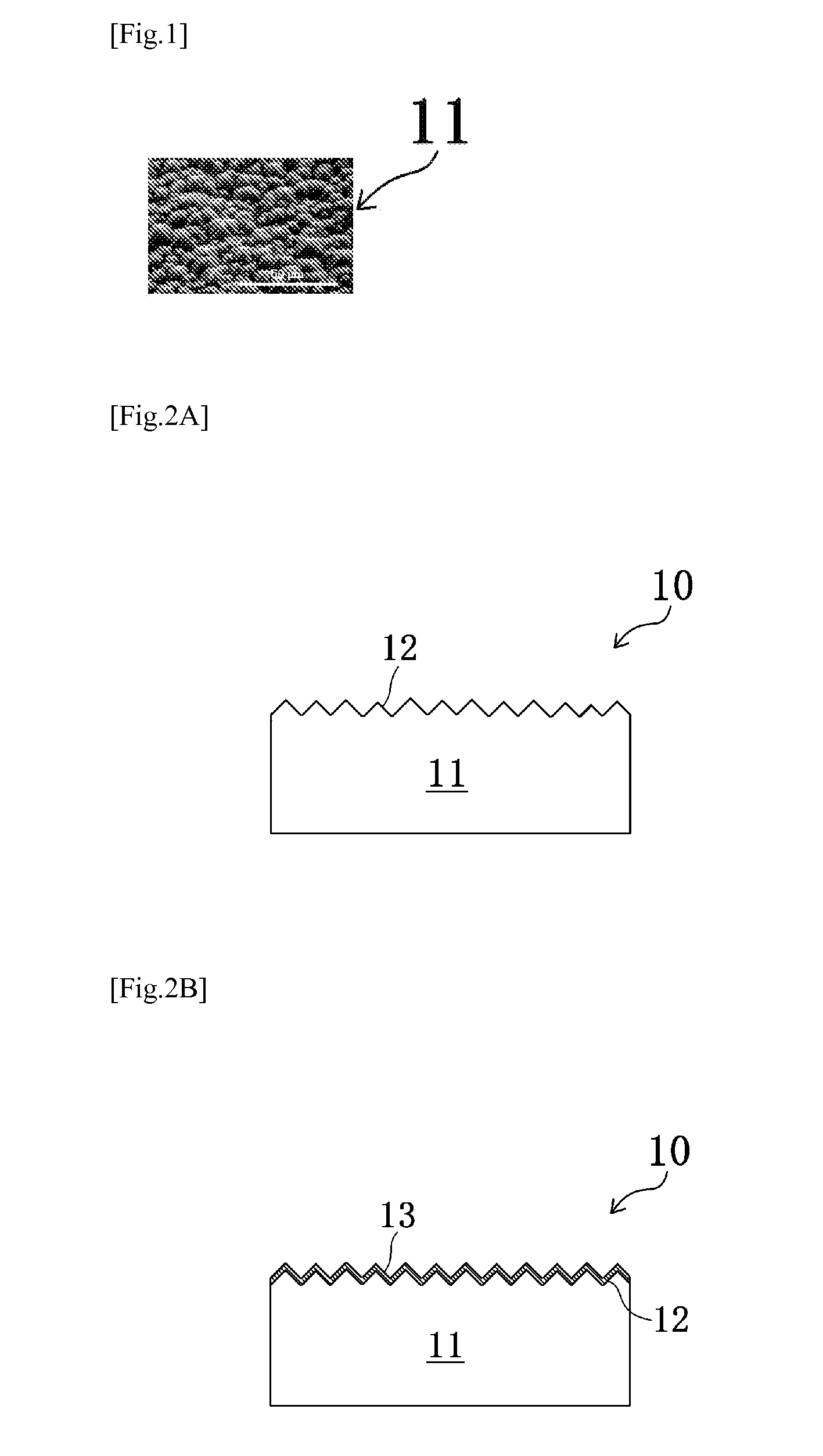
The present invention relates to a method of manufacturing a semiconductor device, an apparatus for manufacturing the semiconductor device, a semiconductor device and a transferring member. In crystalline solar cells, hitherto, attempts to improve energy conversion efficiency by using so-called “optical confinement effect” through converting a flat surface of a silicon substrate to a surface concaved or convexed are made. In this approach, since light reflected once on an inclined surface of the concave and convex is received and taken at the adjacent inclined surface of the concave and convex as distinct from a substrate with a flat surface, the reflectance at the surface can be substantially reduced. As a result of this, since overall quantity of incident light increases, conversion efficiency is increased. As a method of forming the above-mentioned concave and convex structure, for example, there is proposed a method of immersing a silicon substrate into a catalytic metal ion-containing mixed aqueous solution of an oxidizing agent and hydrofluoric acid (Patent Document 1). It is disclosed that in accordance with this method, a porous silicon layer can be formed on the surface of the substrate. However, it cannot be said that the above-mentioned method of forming a concave and convex structure has sufficient controllability of formation of a concave and convex shape. Specifically, it is believed that in the above method, first, a metal on the surface of the silicon substrate is deposited at the surface of the silicon substrate and thereby the metal acts as a decomposition catalyst. Then, since a position or a distribution of metal deposition cannot be freely controlled, it is extremely difficult to ensure the uniformity of a size or distribution of the formed concaves and convexes, and reproducibility thereof is poor. Moreover, it is difficult to eliminate metal after preparing a concave and convex structure of the surface. In addition, the study and development of specific means for forming such uniform concaves and convexes in consideration of the industrial ability or the mass production ability respond to requests of industry. The present invention realizes a surface concaved or convexed, which is excellent in an industrial ability or a mass production ability and is high in uniformity and repeatability, on a semiconductor substrate by solving at least one of the above-mentioned technical problems. As a result of this, the present invention significantly contributes to stable advances in performance of various semiconductor devices typified by solar cells and the industrial realization of these semiconductor devices. One method of the present invention for manufacturing a semiconductor device comprises a supply step of supplying a process liquid that oxidizes and dissolves a semiconductor substrate onto the surface of the semiconductor substrate, a locating step of locating a mesh-like transferring member including a catalyst material at a position in contact with or close to the surface of the semiconductor substrate, and a concave and convex forming step of forming the surface concaved or convexed through the supply step and the locating step. According to the method for manufacturing a semiconductor device, since concaves and convexes of the semiconductor substrate to be subjected to treatment are formed based on a mesh configuration which the transferring member has, a semiconductor device, which includes the semiconductor substrate having concaves and convexes reflecting the mesh configuration of the transferring member, so to speak, as a die or a mold, is attained. That is, it is possible to manufacture stably a semiconductor device including not a semiconductor substrate having highly random, in other words, poorly-reproducible concaves and convexes like conventional concaves and convexes, but a semiconductor substrate having a certain level of a concave and convex shape by forming a proper mesh configuration at a stage of the transferring member. Another method of the present invention for manufacturing a semiconductor device comprises a supply step of supplying a process liquid that oxidizes and dissolves a semiconductor substrate onto the surface of the semiconductor substrate, a locating step of locating a transferring member including a catalyst material on the surface concaved or convexed or above the surface concaved or convexed at a position in contact with or close to the surface of the semiconductor substrate, and a concave and convex forming step of forming the surface concaved or convexed of the semiconductor substrate through the supply step and the locating step. According to the method for manufacturing a semiconductor device, since concaves and convexes of the semiconductor substrate to be subjected to treatment are formed based on a concave and convex shape which the transferring member has, a semiconductor device, which includes the semiconductor substrate having concaves and convexes reflecting the concave and convex shape of the transferring member, so to speak, as a die or a mold, is attained. That is, it is possible to manufacture stably a semiconductor device including not a semiconductor substrate having highly random, in other words, poorly-reproducible concaves and convexes like conventional concaves and convexes, but a semiconductor substrate having a certain level of a concave and convex shape by forming a proper concave and convex shape at a stage of the transferring member. Further, a manufacturing apparatus of a semiconductor device, which is one of the present invention, comprises a supply unit for supplying a process liquid that oxidizes and dissolves a semiconductor substrate onto the surface of the semiconductor substrate, and a locating unit for locating a mesh-like transferring member including a catalyst material at a position in contact with or close to the surface. According to the manufacturing apparatus of a semiconductor device, since concaves and convexes of the semiconductor substrate to be subjected to treatment are formed based on a mesh configuration which the transferring member has, a semiconductor device, which includes the semiconductor substrate having concaves and convexes reflecting the mesh configuration of the transferring member, so to speak, as a die or a mold, can be manufactured. That is, it is possible to manufacture stably a semiconductor device including not a semiconductor substrate having highly random, in other words, poorly-reproducible concaves and convexes like conventional concaves and convexes, but a semiconductor substrate having a certain level of a concave and convex shape by forming a proper mesh configuration at a stage of the transferring member. Further, a manufacturing apparatus of a semiconductor device, which is another one of the present invention, comprises a supply unit for supplying a process liquid that oxidizes and dissolves a semiconductor substrate onto the surface of the semiconductor substrate, and a locating unit for locating a transferring member including a catalyst material on the surface concaved or convexed or above the surface concaved or convexed at a position in contact with or close to the surface of the semiconductor substrate. According to the manufacturing apparatus of a semiconductor device, since concaves and convexes of the semiconductor substrate to be subjected to treatment are formed based on a concave and convex shape which the transferring member has, a semiconductor device, which includes the semiconductor substrate having concaves and convexes reflecting the concave and convex shape of the transferring member, so to speak, as a die or a mold, can be manufactured. That is, it is possible to manufacture stably a semiconductor device including not a semiconductor substrate having highly random, in other words, poorly-reproducible concaves and convexes like conventional concaves and convexes, but a semiconductor substrate having a certain level of a concave and convex shape by forming a proper concave and convex shape at a stage of the transferring member. Further, a transferring member, one of the present invention, is a mesh-like member including a catalyst material, and the transferring member converts the surface of a semiconductor substrate to a surface having a concave and convex shape by locating the catalyst material at a position in contact with or close to the surface of the semiconductor substrate in a state in which a process liquid having an oxidizing property and a dissolving property exists on the surface of the semiconductor substrate. According to the transferring member, since concaves and convexes of the semiconductor substrate to be subjected to treatment are formed based on a mesh structure which the transferring member has, it is possible to supply stably the semiconductor substrate having concaves and convexes reflecting the mesh structure of the transferring member, so to speak, as a die or a mold. Further, a transferring member, another one of the present invention, includes a catalyst material on the surface concaved or convexed or above the surface concaved or convexed, and the transferring member converts the surface of a semiconductor substrate to a surface having a concave and convex shape by locating the catalyst material at a position in contact with or close to the surface of the semiconductor substrate in a state in which a process liquid having an oxidizing property and a dissolving property exists on the surface of the semiconductor substrate. According to the transferring member, since concaves and convexes of the semiconductor substrate to be subjected to treatment are formed based on a concave and convex shape which the transferring member has, it is possible to supply stably the semiconductor substrate having concaves and convexes reflecting the concave and convex shape of the transferring member, so to speak, as a die or a mold. Further, a semiconductor device, one of the present invention, is a semiconductor device in which a surface of a semiconductor substrate without an electrode formed thereon has a porous concave and convex shape formed in a state in which a process liquid that oxidizes and dissolves a semiconductor substrate is introduced onto the surface of the semiconductor substrate and a mesh-like transferring member including a catalyst material is in contact with or close to the surface. According to the semiconductor device, since concaves and convexes of the semiconductor substrate to be subjected to treatment are formed based on a mesh configuration which the transferring member has, a semiconductor device including the semiconductor substrate having concaves and convexes reflecting the mesh configuration of the transferring member, so to speak, as a die or a mold, is formed. That is, it is possible to attain a semiconductor device including not a semiconductor substrate having highly random, in other words, poorly-reproducible concaves and convexes like conventional concaves and convexes, but a semiconductor substrate having a certain level of a concave and convex shape by forming a proper mesh configuration at a stage of the transferring member. Further, in the above-mentioned inventions, the transferring member is preferably made of a material resistant (typically, etching resistance or insolubility) to a process liquid having an oxidizing property and a dissolving property in forming concaves and convexes of the surface of the semiconductor substrate by liberating such a process liquid to the semiconductor substrate to be subjected to treatment. The transferring member is not particularly limited, and a crystalline semiconductor substrate or a member having a mesh structure can be employed as a transferring member. In addition, concaves and convexes in the transferring member are not limited to the case where the concaves and convexes are formed by using wet chemical etching. For example, a fine concave and convex shape formed by isotropic or anisotropic dry etching or nanoimprinting, based on a semiconductor technology or a MEMS technology, can be applied. Further, in the above-mentioned inventions, the mesh-like member is not limited to the case where a member is formed in the form of intersecting vertical line and horizontal line (for example, net-like), typified by The present inventor assumes a mechanism which forms concaves and convexes of the semiconductor substrate to be as follows. First, when a surface concaved or convexed at the surface of the transferring member or a catalyst material existing on the mesh structure is brought into contact with the surface of the semiconductor substrate, the catalyst material acts as a cathode of an electrochemical reaction and a decomposition reaction of an oxidizing agent occurs at the surface of the catalyst material. On the other hand, an anode reaction occurs at the surface of a silicon surface. As a highly potential anode reaction, the following reaction formula is conceivable. It is thought that for example, in the case where the above-mentioned mesh-like transferring member is employed, the silicon surface is dissolved by the above anode reaction to form a porous silicon. More specifically, the present inventor assumes that since hydrogen ions (H+) are produced by the above reaction, equilibrium shifts to the right side by increasing a pH, that is, by making the reaction alkaline, and therefore a reaction of forming a porous silicon proceeds. That is, addition of alkali can promote a reaction of forming a porous silicon. Further, if a catalyst material acts as a decomposition catalyst of the oxidizing agent in the process liquid at the surface of the semiconductor substrate, an atomic oxygen produced from the oxidizing agent oxidizes the surface of the semiconductor substrate. Then, an oxide layer of the oxidized site is dissolved by a dissolving agent, and therefore the surface of the semiconductor is substantially etched. Oxidation of the surface of the semiconductor substrate and dissolution of the surface of the semiconductor substrate in the process liquid are repeated, and a concave and convex shape substantially reflecting the configuration of the surface of the transferring member, in other words, a concave and convex shape, in which the configuration of the surface of the transferring member is reversed, is probably formed. Therefore, in the above-mentioned inventions, the catalyst material is not particularly limited as long as it acts as a decomposition catalyst of the oxidizing agent in the above-mentioned process liquid. Daresaying, typical preferred examples of the catalyst material include at least one selected from the group consisting of platinum (Pt), silver (Ag), palladium (Pd), gold (Au), rhodium (Rh) and alloys containing these metals. In the present application, “the transferring member includes the catalyst material” is a concept including a state in which a film or a layer of the catalyst material is formed on the surface of the transferring member, and a state in which the catalyst material adheres onto the surface of the transferring member in the form of a particle or an island, and including various aspects in which the catalyst material on the transferring member can develop a function or performance as a catalyst. Moreover, the meaning of “a transferring member includes a catalyst material” includes an aspect in which even though the transferring member itself can contain unavoidable impurities, transferring member is composed of only the catalyst material. In addition, a typical aspect of such a catalyst material is a film formed by a publicly known sputtering method, a vapor-deposited film by a CVD method or the like, or a film formed by plating, but the catalyst material is not limited to these films. According to the method for manufacturing a semiconductor device, one of the present invention, since concaves and convexes of the semiconductor substrate to be subjected to treatment are formed based on a concave and convex shape or a mesh configuration which the transferring member has, a semiconductor device, which includes the semiconductor substrate having concaves and convexes reflecting the concave and convex shape or the mesh configuration of the transferring member, so to speak, as a die or a mold, is attained. That is, it is possible to manufacture stably a semiconductor device including not a semiconductor substrate having highly random, in other words, poorly-reproducible concaves and convexes like conventional concaves and convexes, but a semiconductor substrate having a certain level of a concave and convex shape by forming a proper concave and convex shape or mesh configuration at a stage of the transferring member. Further, according to the manufacturing apparatus of a semiconductor device, one of the present invention, since concaves and convexes of the semiconductor substrate to be subjected to treatment are formed based on a concave and convex shape or a mesh configuration which the transferring member has, a semiconductor device, which includes the semiconductor substrate having concaves and convexes reflecting the concave and convex shape or the mesh configuration of the transferring member, so to speak, as a die or a mold, can be manufactured. That is, it is possible to manufacture stably a semiconductor device including not a semiconductor substrate having highly random, in other words, poorly-reproducible concaves and convexes like conventional concaves and convexes, but a semiconductor substrate having a certain level of a concave and convex shape by forming a proper concave and convex shape or mesh configuration at a stage of the transferring member. Further, according to the transferring member, one of the present invention, since concaves and convexes of the semiconductor substrate to be subjected to treatment are formed based on a concave and convex shape or a mesh structure which the transferring member has, it is possible to supply stably the semiconductor substrate having concaves and convexes reflecting the concave and convex shape or the mesh structure of the transferring member, so to speak, as a die or a mold. Next, an embodiment of the present invention will be described in detail based on the attached drawings. In addition, in this description, parts are given as reference characters throughout all drawings unless otherwise specified. In addition, in drawings, elements in the present embodiment are not necessarily drawn with the same scales. In the present embodiment, at first, a method of manufacturing a transferring member 10 for forming the surface of a semiconductor substrate (substrate to be subjected to a treatment, hereinafter, also referred to as a “substrate to be treated”) to be used for a semiconductor device (a solar cell in the present embodiment) into a concave and convex shape will be described. In manufacturing of the transferring member 10, at first, a monocrystalline n-type silicon (100) substrate (resistivity: 1 to 20 Ωcm) subjected to surface washing treatment by the so-called RCA washing method is immersed in a mixed aqueous solution of sodium hydroxide (NaOH) having a molar concentration of 0.25 mol/dm3and 2-propanol having a molar concentration of 0.6 mol/dm3for 20 minutes. Next, as shown in In the present embodiment, as shown in By the way, the silicon nitride film 15 is used as the so-called intermediate layer which functions as a protective film of the n-type silicon substrate 11 in the transferring member 10, or as an impermeable layer against a process liquid described later. Therefore, the silicon nitride film 15 can also function as the peel-preventive layer of a catalyst material 17 described later. In the present embodiment, as described above, laminating two layers of the oxide film 13 and the silicon nitride film 15 largely contributes to the stability and reliability of the transferring member 10 since the catalyst material 17 is prevented from peeling off and resistance to the process liquid described later is improved. Next, as shown in Subsequently, the n-type silicon substrate 11, in which a film of the catalyst material 17 is formed on the above-mentioned surface 12 with pyramid-like convexes and concaves, is used as a transferring member 10, and a concave and convex shape of a semiconductor substrate to be subjected to treatment was formed. In the present embodiment, a locating unit, which opposes the above surface 12 with pyramid-like convexes and concaves to the substrate 20 to be treated, and locates the transferring member 10 including a catalyst material 17 at a position in contact with or close to the substrate 20 to be treated, is disposed. The top of a convex of the platinum film surface of the catalyst material 17 has been subjected to surface washing treatment by the RCA washing method in order to avoid the contamination of the surface of the substrate 20. Thereafter, a mixed aqueous solution of hydrofluoric acid (HF) as a dissolving agent and a hydrogen peroxide solution (H2O2) as an oxidizing agent is supplied as a process liquid 19 between the surface of the substrate 20 to be treated and the platinum film of the catalyst material 17 ( The substrate 20 to be treated was maintained at 25° C. for 2 hours under the above-mentioned condition, and then the surface of the substrate 20 to be treated was observed. Consequently, as shown in By the way, in the present embodiment, an oxide film (SiO2) 13 and a silicon nitride (Si3N4) film 15 are formed on the surface of an n-type silicon substrate 11, but First Embodiment is not limited to this laminated structure. For example, Even when such a transferring member 10 In addition to Variation Example (1) of First Embodiment, for example, even a laminate in which only an oxide film (SiO2) 13 is formed on the surface of the n-type silicon substrate 11, or even a transferring member in which a catalyst material 17 is directly placed on the surface of the n-type silicon substrate 11 can achieve at least a part of the effect of First Embodiment. However, from the viewpoint of preventing the catalyst material 17 from peeling off from the n-type silicon substrate 11 and from the viewpoint of protecting the n-type silicon substrate 11 itself from dissolution, other two aspects other than the transferring member in which the catalyst material 17 is directly placed on the surface of the n-type silicon substrate 11 are more preferred, and it is most preferred to employ a structure in which the oxide film (SiO2) 13 and the silicon nitride (Si3N4) film 15 are formed as with First Embodiment. A surface concaved or convexed of a substrate to be treated in the present embodiment is formed by the same manufacturing method of a transferring member 10 and a substrate 20 to be treated as in First Embodiment except that the substrate 20 to be treated in First Embodiment is a monocrystalline silicon (111) substrate. Therefore, a description duplicating that in First Embodiment can be omitted. A surface concaved or convexed of a substrate to be treated in the present embodiment is formed by the same manufacturing method of a transferring member 10 and a substrate 20 to be treated as in First Embodiment except that the substrate 20 to be treated is a polycrystalline silicon (poly-Si) substrate and the treatment time by a process liquid 19 in First Embodiment is different. Therefore, a description duplicating that in First Embodiment can be omitted. In the present embodiment, a polycrystalline silicon (Poly-Si) substrate, a substrate 20 to be treated, was immersed in the process liquid 19 for 4 hours. Further, In the present embodiment, an i-type a-Si layer 31 and a p+-type a-Si layer 32 are laminated and formed on the n-type polycrystalline silicon substrate 30 having a surface concaved or convexed formed by Third Embodiment described above by using a publicly known film forming technology (e.g., plasma chemical vapor deposition (PCVD) method). Thereafter, in the present embodiment, an ITO film, a transparent conductive film, is formed on the p+-type a-Si layer 32 as surface electrode layers 34, for example, by a publicly known sputtering method. Further, an n+-type a-Si layer of a backside electrode layer 36 is formed on the opposite side of the polycrystalline silicon substrate 30 by a publicly known film forming technology (e.g., plasma chemical vapor deposition (PCVD) method). As shown in Explaining with reference to By the way, in Embodiments described above, as typically shown in For example, the case where after the process liquid 19 is supplied onto the surface of the substrate 20 to be treated, it can be employed to locate the transferring member 10 at a position in contact with or close to the substrate 20 to be treated. When this procedure is employed, since the difficulty of spreading the process liquid 19 uniformly through a gap between the surface of the substrate 20 to be treated and the catalyst material 17 is resolved, this is a preferred aspect. In addition, in the above-mentioned embodiments, as shown in A surface concaved or convexed of a substrate to be treated in the present embodiment is formed by the same manufacturing method as in First Embodiment except that mainly, a mesh-like transferring member shown in The mesh-like transferring member 10 In the present embodiment, the mesh-like transferring member 10 As a result of this, a substrate 20 to be treated, on which concaves and convexes reflecting a shape of the mesh-like transferring member 10 As shown in A surface concaved or convexed of a substrate to be treated in the present embodiment is formed by the same manufacturing method as in First Embodiment except that mainly, a mesh-like transferring member 10 As shown in Therefore, in the present embodiment, after the process liquid 19 of 60° C. is supplied onto the surface of the substrate 20 to be treated, different parts of the mesh-like transferring member 10 Further, the material of the roll body 57 As a result of the above treatment, as schematically shown in Then, the reflectance of the surface of the substrate 20 to be treated in the present embodiment was investigated, and consequently a very interesting result was obtained. As shown in Moreover, the present inventor made investigations concerning a carrier lifetime of the surface of the substrate 20 to be treated in the present embodiment. Consequently, although the surface of the substrate 20 to be treated of the present embodiment became porous and the surface area of the substrate increased outstandingly, the rate of decrease in a carrier lifetime was only 10% or less. This particularly worth noting result differs from the result of the surface of the texture structure employed in the transferring substrate 10. For example, in a texture structure employed in the transferring substrate 10, which is formed on the surface of a monocrystalline silicon (100), the rate of decrease in a lifetime is 50% or more since a face having a high interface state density (111) is exposed. On the other hand, it was verified that in the substrate 20 to be treated of the present embodiment, the rate of decrease in a lifetime can be reduced to 10% or less. A surface concaved or convexed of a substrate to be treated in the present embodiment is formed by the same manufacturing method as in Sixth Embodiment except that the temperature and the concentration of the process liquid 19 in Sixth Embodiment were changed and the material of the mesh-like transferring member 10 The substrate 20 to be treated was subjected to the same treatment as in Sixth Embodiment under the above-mentioned conditions. In addition, the manufacturing apparatus 51 of a semiconductor device of the present embodiment and a manufacturing method thereof also have such an excellent industrial ability or an excellent mass production ability as to treat such a substrate 20 to be treated in about 5 seconds if the substrate 20 to be treated is a monocrystalline silicon wafer having a diameter of 6 inches as with Sixth Embodiment. As shown in A surface concaved or convexed of a substrate to be treated in the present embodiment is formed by the same manufacturing method as in Sixth Embodiment except that a crystal orientation of the substrate 20 to be treated was changed. Therefore, a description duplicating those in First Embodiment, Fifth Embodiment and Sixth Embodiment can be omitted. In addition, the substrate 20 to be treated of the present embodiment is a monocrystalline silicon (111) substrate. A surface concaved or convexed of a substrate to be treated in the present embodiment is formed by the same manufacturing method as in Sixth Embodiment except that the manufacturing apparatus 51 of a semiconductor device of Sixth Embodiment was changed to a manufacturing apparatus 52 of a semiconductor device. Therefore, a description duplicating those in First Embodiment and Sixth Embodiment can be omitted. In addition, with respect to a shape of the roll body 57 By the way, the substrate to be treated was a monocrystalline silicon substrate or a polycrystalline silicon substrate in Embodiments described above, but the substrate 20 to be treated is not limited to this. For example, even when the substrate 20 to be treated is a semiconductor substrate such as silicon carbide (SiC), GaAs or InGaAs, the same effect as in Embodiments described above can be achieved. In addition, also the transferring member 10 is not limited to the n-type silicon substrate. For example, even when the substrate 20 to be treated is a silicon substrate other than the n-type silicon substrate, a silicon carbide (SiC) substrate, a metal thin film substrate, a polymer resin or a flexible substrate, the same effects as in Embodiments described above can be achieved. In Embodiments described above, platinum (Pt) was employed as the catalyst material 17, but the catalyst material 17 is not limited to platinum. For example, as the catalyst material 17, a material, which is at least one selected from the group consisting of silver (Ag), palladium (Pd), gold (Au), rhodium (Rh), ruthenium (Ru), iridium (Ir), and alloys containing at least one of them, and acts as a decomposition catalyst of the oxidizing agent (e.g., hydrogen peroxide) in the process liquid 19, is used. For example, even when the catalyst material is an alloy which is predominantly composed of gold (Au) and contains palladium (Pd) and platinum (Pt), an alloy which is predominantly composed of gold (Au) and contains palladium (Pd), an alloy which is predominantly composed of gold (Au) and contains silver (Ag) and copper (Cu), an alloy which is predominantly composed of gold (Au) and contains silver (Ag), copper (Cu) and palladium (Pd), an alloy of molybdenum (Mo), tungsten (W), iridium (Ir) and platinum (Pt), or an alloy of iron (Fe), cobalt (Co), nickel (Ni) and platinum (Pt), at least a part of the effects of Embodiments described above can be exerted. In addition to this, a small amount of another metal in the above-mentioned catalyst materials may be added. For example, those skilled in the art may appropriately add a proper metal in order to enhance wear resistance or durability. Moreover, in Sixth Embodiment and Variation Examples of Sixth Embodiment, it is a more preferred aspect to select, as a catalyst material, noble metals less prone to being oxidized by an influence of particularly a high concentration of an oxidizing agent in the process liquid 19, that is, a hydrogen peroxide solution (H2O2), for example, at least one selected from the group consisting of platinum (Pt), palladium (Pd), rhodium (Rh), gold (Au) and alloys containing them, because catalyst performance is easily maintained. In addition, the meaning of “alloy” in this paragraph is similar to that in description of the above-mentioned catalyst material 17. In addition to this, a catalyst substance (i.e., catalyst material 17) contributing to promotion of oxidation is not limited the above-mentioned metals. For example, other publicly known catalyst substances including oxide compounds, carbon alloy compounds and inorganic compounds, and various complexes having functions equal to those of the above-mentioned compounds can be employed. In First Embodiment to Third Embodiment, it is a preferred aspect to interpose an interlayer functioning as a peel-preventive layer to enhance the adhesion like First Embodiment or as an impermeable layer against the process liquid 19 between a matrix substrate (the n-type silicon substrate 11 in First Embodiment) of the transferring member 10 and the catalyst material 17, as required. Further, in any of Embodiments described above, the aspect, in which the transferring member includes the catalyst material, includes a state in which a film or a layer of the catalyst material is formed on the surface of the transferring member, and a state in which the catalyst material adheres onto the surface of the transferring member in the form of a particle or an island, and includes various aspects in which the catalyst material on the transferring member can develop a function or performance as a catalyst. As a metal serving as the above-mentioned catalyst material 17, typically, a vapor deposition film formed by a publicly known method such as a sputtering method, a plating method or a CVD method, or a film formed by reducing a coat prepared by applying a compound can be employed, but Embodiments described above are not limited to these films. Further, in Embodiments described above, a mixed aqueous solution of hydrofluoric acid (HF) and a hydrogen peroxide solution (H2O2) was used as the process liquid 19, but the process liquid 19 is not limited to this mixed aqueous solution. For example, by employing a mixed aqueous solution of hydrofluoric acid (HF) and at least one oxidizing agent selected from the group consisting of a hydrogen peroxide solution (H2O2), an aqueous solution of potassium dichromate (K2Cr2O7), an aqueous solution of potassium manganate (KMnO4), nitric acid (HNO3), sulfuric acid (H2SO4), and water containing oxygen (O2) or ozone (O3) dissolved therein, as a process liquid 19, at least a part of the effects (e.g., formation of a porous surface) of Embodiments described above is exerted. Further, also when various highly oxidizing solutions or ozone water is employed as an example of the process liquid 19 described above, it is preferred to select noble metals less prone to being oxidized by the process liquid 19 as a catalyst material particularly in Sixth Embodiment and Variation Examples of Sixth Embodiment. The example of the solar cell 100 in Fourth Embodiment described above can be applied to First Embodiment, Second Embodiment, Fifth Embodiment, Sixth Embodiment, and other Embodiment. Particularly, in Sixth Embodiment and Variation Examples of Sixth Embodiment, since the surface of the substrate 20 to be treated becomes porous, the surface area of the substrate 20 to be treated significantly increases, and the short-circuit current (JSC) value which contributes to photoelectric conversion efficiency of a solar cell is improved because of significantly low reflectance of light. Moreover, it is particularly worth noting that a high open voltage (VOC) can be attained since reduction in a carrier lifetime is suppressed regardless of outstanding increase in surface area. Further, the base materials of the mesh-like transferring members 10 Moreover, as an aspect of another solar cell prepared by applying Sixth Embodiment and Variation Examples of Sixth Embodiment, the following structure can be employed. First, after a shape of a part in the mesh-like transferring member where a mesh of the mesh-like transferring member is not present is formed into a shape of a comb-like (typically, in a plan view) surface electrode of a silicon solar cell commonly employed in advance, treatments in Sixth Embodiment are performed. Then, a convex portion corresponding to the comb-like surface electrode and concave portions reflecting a configuration of the mesh-like transferring member are formed on the surface of a silicon substrate, a substrate 20 to be treated. As a result of this, the concave portion reflecting a configuration of the mesh-like transferring member and a surface around the concave portion become porous, but a surface of the convex portion corresponding to the comb-like surface electrode does not become porous. Thereafter, by forming a silver electrode on the surface of the convex portion corresponding to the comb-like surface electrode by a publicly known technique, a solar cell is prepared. In accordance with such a solar cell, for example, when the substrate to be treated has a flat surface, it becomes easy to form an electrode since a silver electrode can be formed on the flat surface, and on the other hand, in a region other than the electrode, an improvement in the short-circuit current (JSC) value and a high open voltage (VOC) by virtue of the effect of suppressing reduction in a carrier life time can be simultaneously realized. Further, in any of Embodiments described above, it is another preferred aspect that not only the polycrystalline silicon substrate of Fourth Embodiment, but also a monocrystalline silicon substrate or the above-mentioned amorphous silicon substrate is employed as a substrate 20 to be treated which is employed as a solar cell. In addition to this, in Fourth Embodiment, Sixth Embodiment and Variation Examples of Sixth Embodiment described above, the solar cell was described as an example of the semiconductor device, but the example of the semiconductor device is not limited to the solar cell. For example, treatments of forming a concave and convex shape by use of the transferring members 10, 10 In addition, disclosure of Embodiments described above is described for explanations of these Embodiments, and is not described for limiting the present invention to these Embodiments. In addition, variation examples, including another combination of Embodiments, within the scope of the present invention are also intended to be embraced by the claims. The present invention can largely contribute to realization of improvement in performance and higher functionality of a substrate to be treated prepared by using a transferring member and hence a semiconductor device manufactured by using the substrate to be treated. Accordingly, the present invention can be used widely in the field of semiconductor devices typified by optical devices such as solar cells, light-emitting devices and light-receiving devices. Disclosed is a method for manufacturing semiconductor devices. Said method includes: a supply step in which a process liquid (19) that oxidizes and dissolves a target substrate (20) to be treated is supplied to the surface of said substrate (20) to be treated; a positioning step in which a mesh-like transferring member (10b) provided with a catalyst material is positioned near or in contact with the surface of the substrate (20) to be treated; and a concave or convex forming step in which a concave or convex is formed on the surface of the substrate (20) to be treated via the aforementioned supply and positioning steps. As opposed to existing manufacturing methods, which manufacture semiconductor devices provided with semiconductor substrates with highly arbitrary (i.e. not very reproducible) concaves or convexes, by forming an appropriate concave or convex or mesh at the transferring member step, the disclosed method can stably manufacture semiconductor devices provided with semiconductor substrates that have concaves or convexes of a fixed level. 1. A method for manufacturing a semiconductor device comprising:
a supply step of supplying a process liquid that oxidizes and dissolves a semiconductor substrate onto the surface of the semiconductor substrate; a locating step of locating a mesh-like transferring member including a catalyst material at a position in contact with or close to the surface; and a concave and convex forming step of forming the surface concaved or convexed through the supply step and the locating step. 2. A method for manufacturing a semiconductor device comprising:
a supply step of supplying a process liquid that oxidizes and dissolves a semiconductor substrate onto the surface of the semiconductor substrate; a locating step of locating a transferring member including a catalyst material on the surface concaved or convexed or above the surface concaved or convexed at a position in contact with or close to the surface of the semiconductor substrate; and a concave and convex forming step of forming the surface concaved or convexed of the semiconductor substrate through the supply step and the locating step. 3. The method for manufacturing a 1 semiconductor device according to 4. The method for manufacturing a semiconductor device according to 5. The method for manufacturing a semiconductor device according to 6. The method for manufacturing a semiconductor device according to 7. The method for manufacturing a 1 semiconductor device according to 8. The method for manufacturing a semiconductor device according to 9. The method for manufacturing a semiconductor device according to 10. The method for manufacturing a semiconductor device according to 11. A manufacturing apparatus of a semiconductor device comprising:
a supply unit for supplying a process liquid that oxidizes and dissolves a semiconductor substrate onto the surface of the semiconductor substrate; and a locating unit for locating a mesh-like transferring member including a catalyst material at a position in contact with or close to the surface. 12. A manufacturing apparatus of a semiconductor device comprising:
a supply unit for supplying a process liquid that oxidizes and dissolves a semiconductor substrate onto the surface of the semiconductor substrate; and a locating unit for locating a transferring member including a catalyst material on the concaved or convexed surface or above the concaved or convexed surface at a position in contact with or close to the surface of the semiconductor substrate. 13. The manufacturing apparatus of a semiconductor device according to 14. The manufacturing apparatus of a semiconductor device according to 15. A transferring member, wherein the transferring member is a mesh-like member including a catalyst material, and the transferring member converts the surface of a semiconductor substrate to a surface having a concave and convex shape by locating the catalyst material at a position in contact with or close to the surface of the semiconductor substrate in a state in which a process liquid having an oxidizing property and a dissolving property exists on the surface of the semiconductor substrate. 16. A transferring member, wherein the transferring member includes a catalyst material on the surface concaved or convexed or above the surface concaved or convexed, and the transferring member converts the surface of a semiconductor substrate to a surface having a concave and convex shape by locating the catalyst material at a position in contact with or close to the surface of the semiconductor substrate in a state in which a process liquid having an oxidizing property and a dissolving property exists on the surface of the semiconductor substrate. 17. The transferring member according to 18. A semiconductor device, wherein a surface of a semiconductor substrate without an electrode formed thereon has a porous concave and convex shape formed in a state in which a process liquid that oxidizes and dissolves the semiconductor substrate is introduced onto the surface of the semiconductor substrate and a mesh-like transferring member including a catalyst material is in contact with or close to the surface. 19. The semiconductor device according to 20. The method for manufacturing a semiconductor device according to 21. The method for manufacturing a semiconductor device according to 22. The method for manufacturing a semiconductor device according to 23. The method for manufacturing a semiconductor device according to TECHNICAL FIELD
BACKGROUND ART
PRIOR ART DOCUMENTS
Patent Documents
DISCLOSURE OF THE INVENTION
Problems to be Solved by the Invention
Solutions to the Problems
Si+6HF+2Effects of the Invention
BRIEF DESCRIPTION OF THE DRAWINGS
DESCRIPTION OF REFERENCE SIGNS
EMBODIMENTS OF THE INVENTION
First Embodiment
Variation Example (1) of First Embodiment
Variation Example (2) of First Embodiment
Second Embodiment
Third Embodiment
Fourth Embodiment
Other Variation Examples of First Embodiment to Fourth Embodiment
Fifth Embodiment
Sixth Embodiment
Variation Example (1) of Sixth Embodiment
Variation Example (2) of Sixth Embodiment
Variation Example (3) of Sixth Embodiment
Other Embodiments
INDUSTRIAL APPLICABILITY