SUBSTRATE, METHOD FOR FABRICATING THE SAME, AND DISPLAY DEVICE
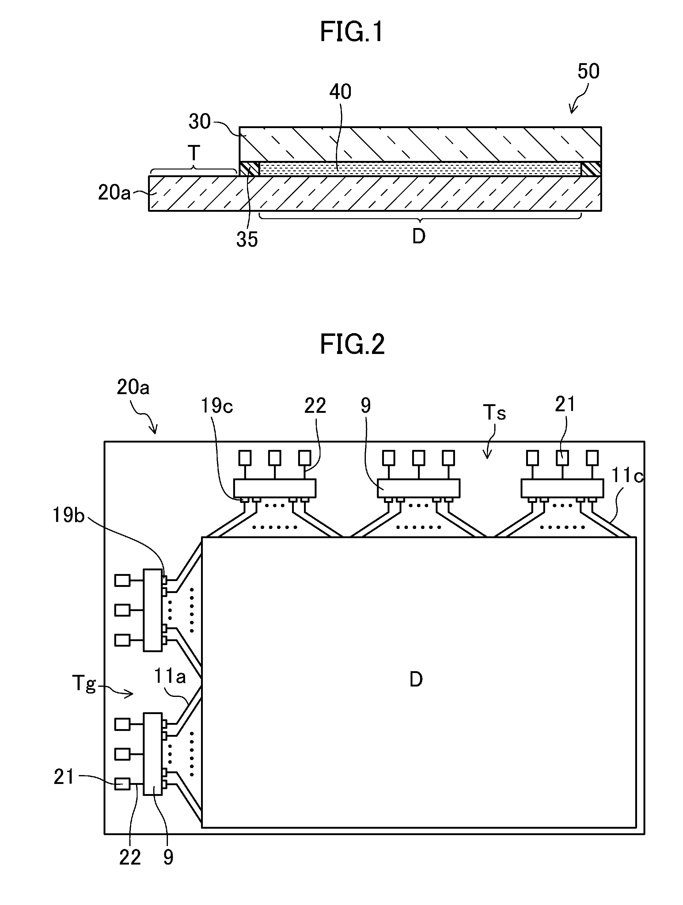
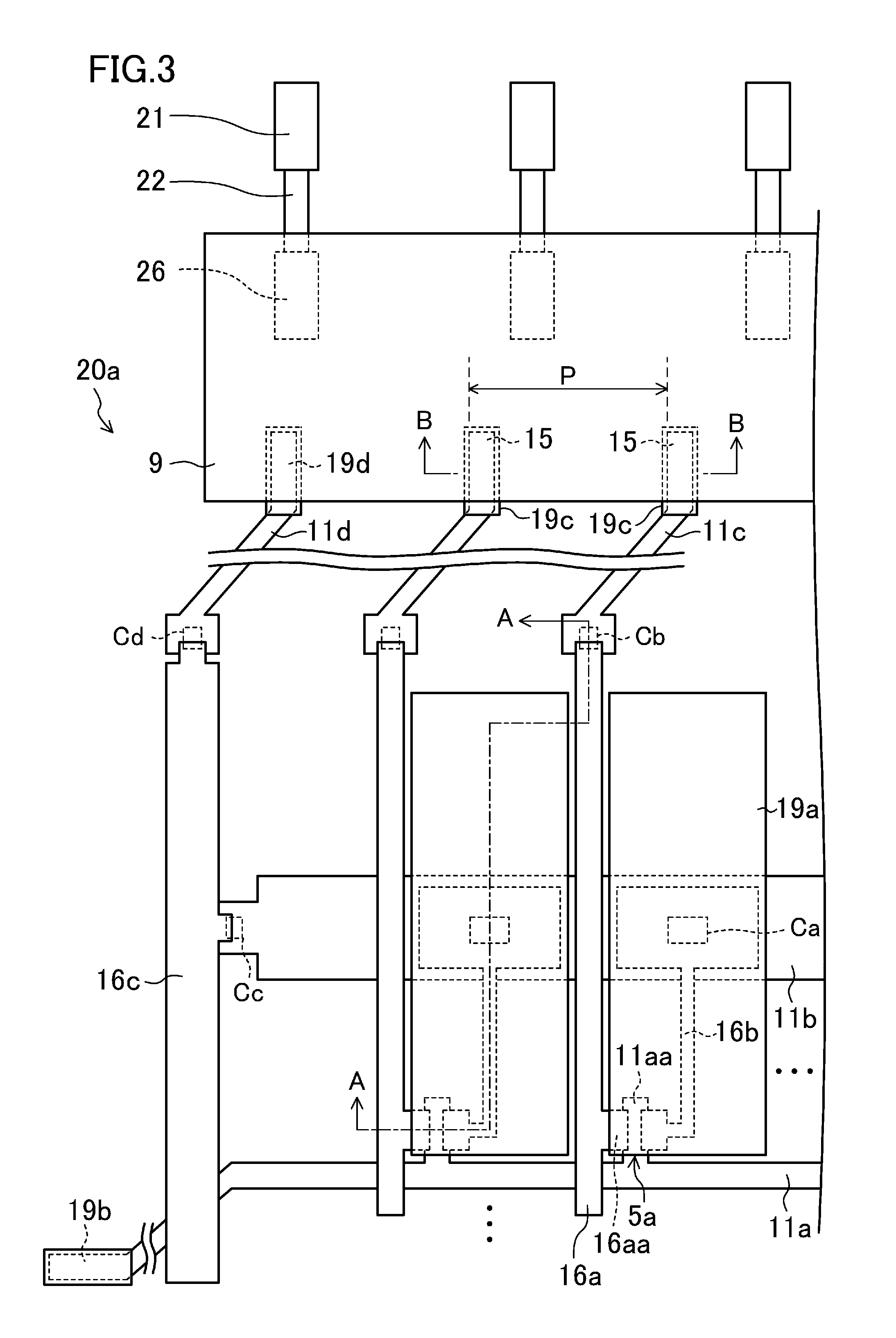
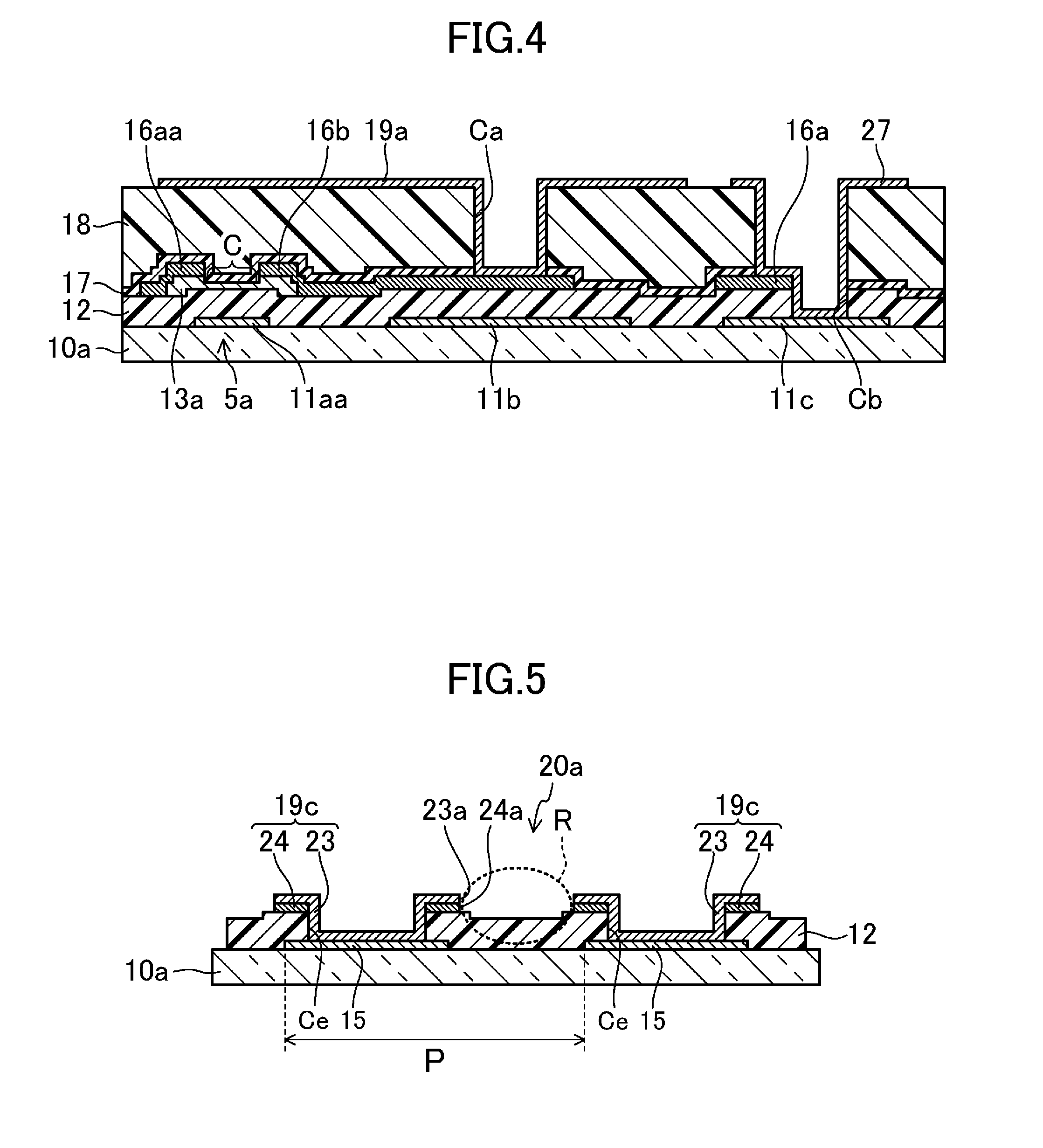
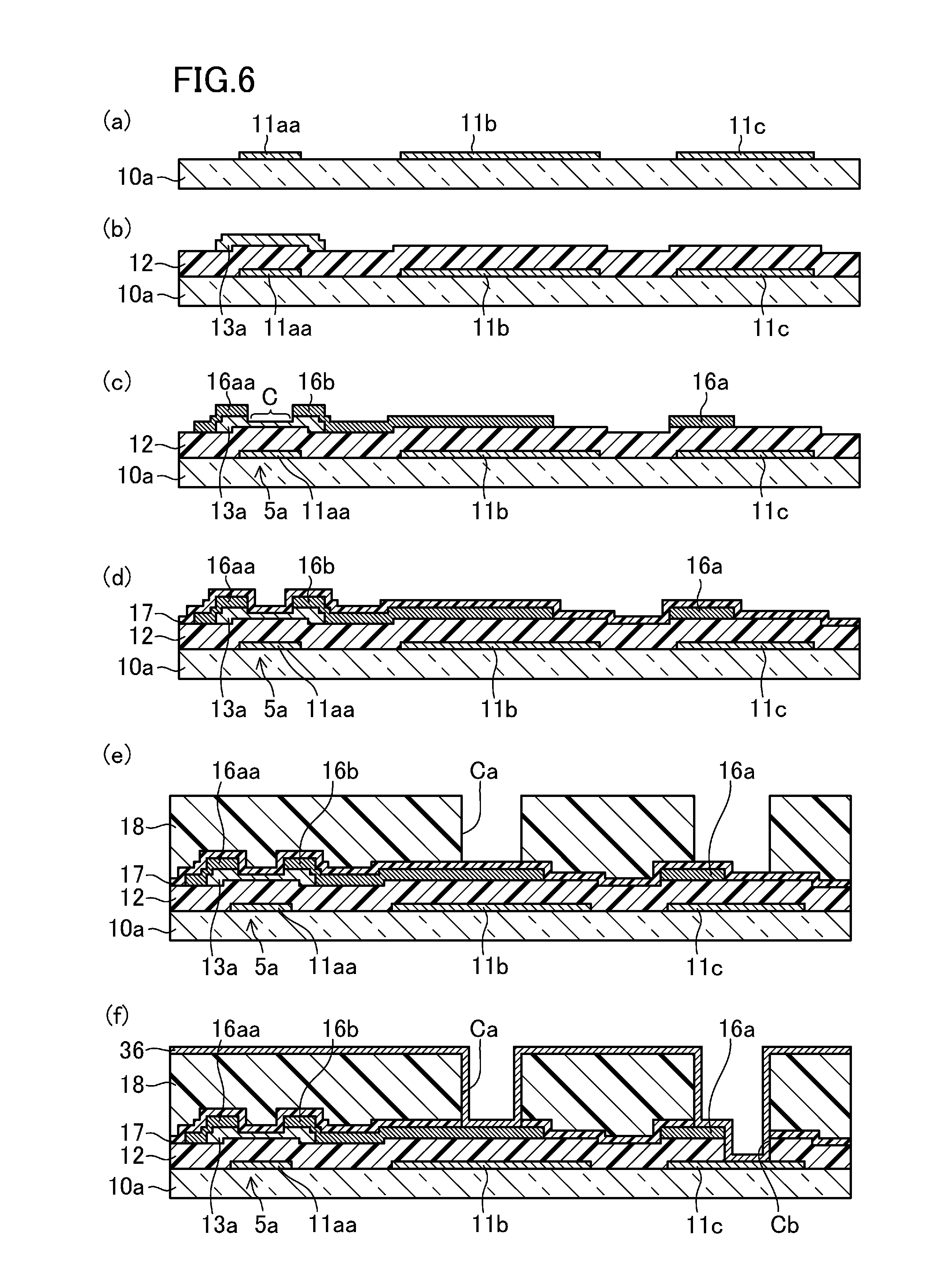
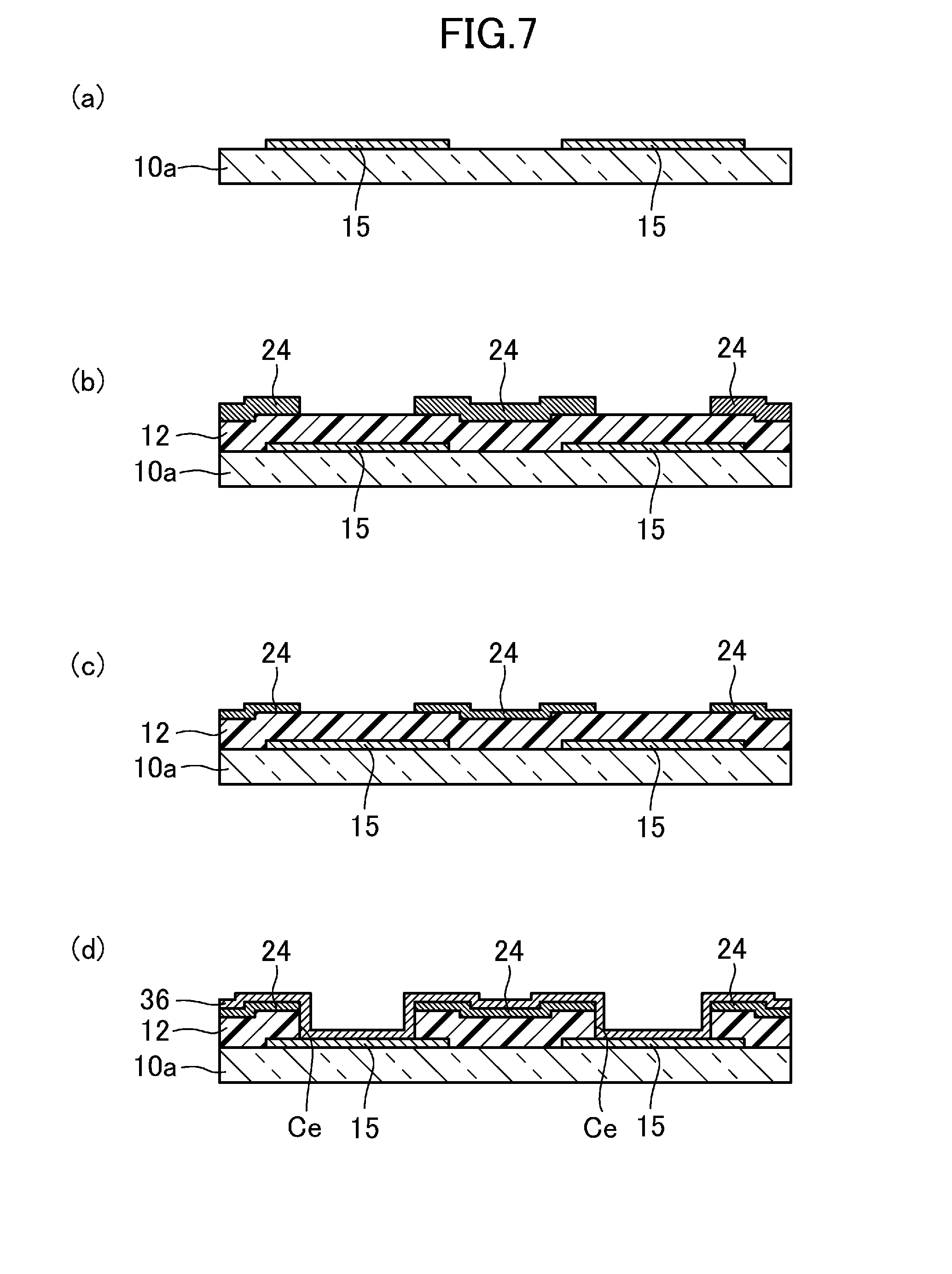
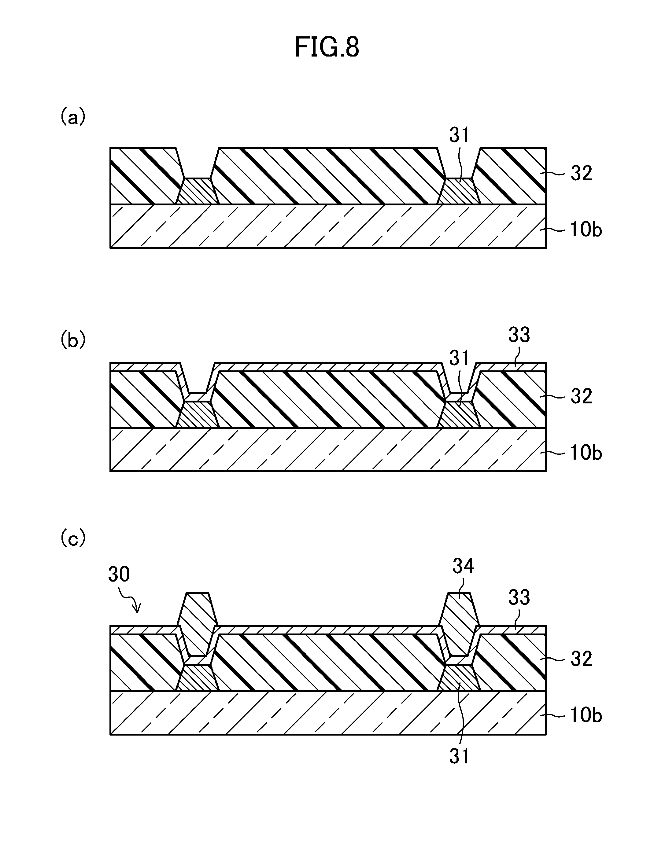
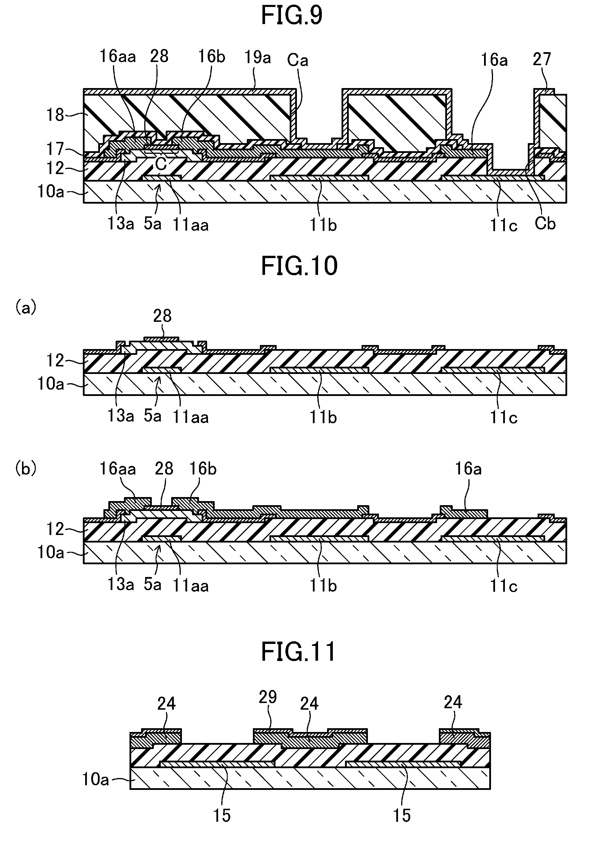
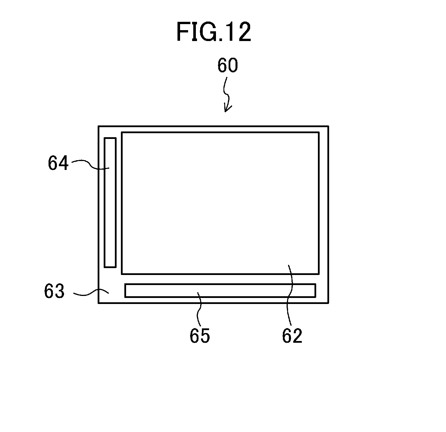
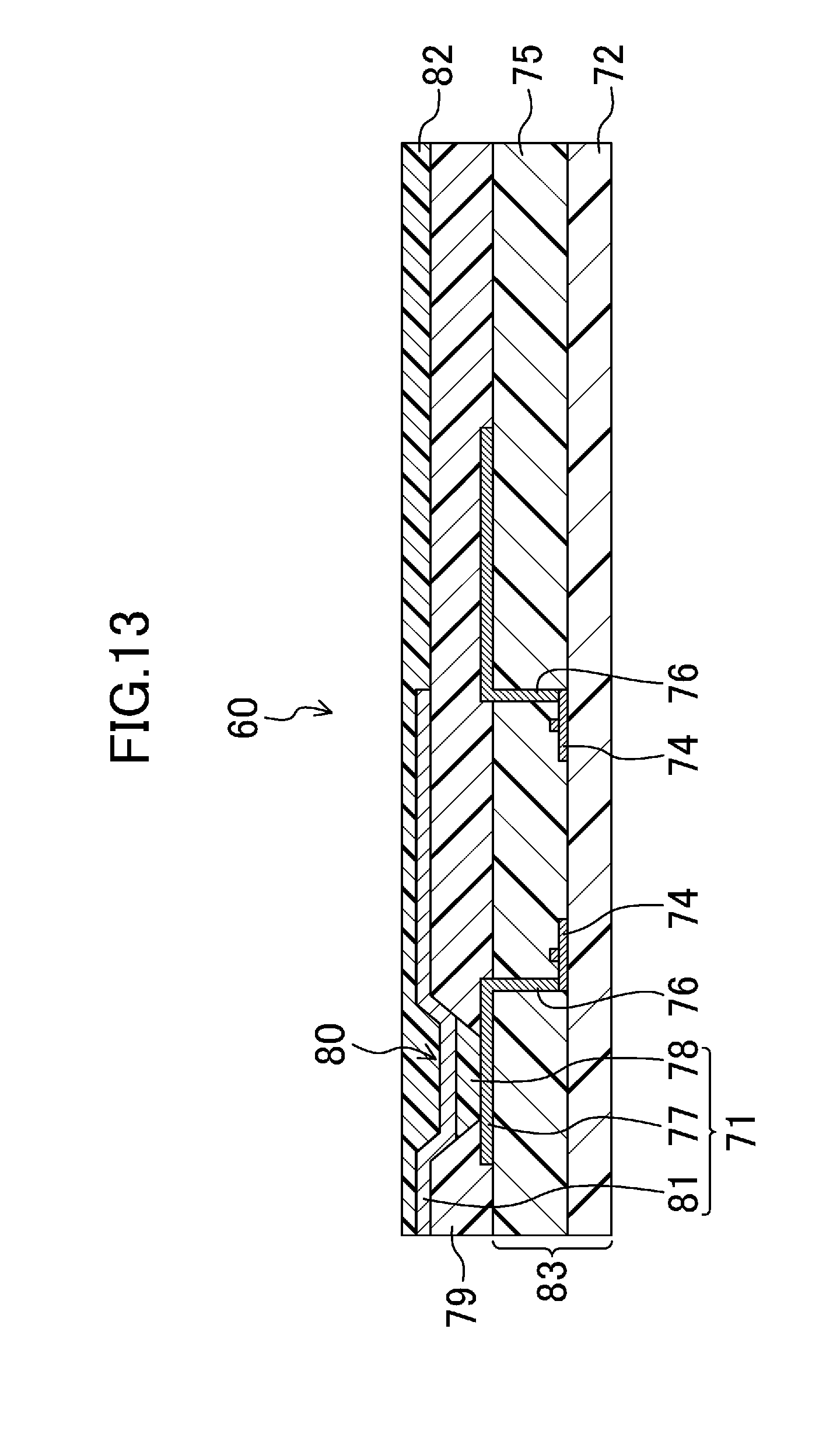
The present disclosure generally relates to substrates, and more particularly to a substrate including a semiconductor layer of an oxide semiconductor, a method for fabricating the substrate, and a display device. Liquid crystal display devices having the advantages of small thickness, lightweight, drivability at low voltages, and low power consumption have been recently used as display panels of various types of mobile terminal devices, e.g., cell phones and portable game devices, and electronic equipment, e.g., laptop computers. In general, a liquid crystal display device includes a pair of opposing substrates (i.e., a thin-film transistor substrate and a counter substrate), a liquid crystal layer provided between the substrates, and a sealing material bonding the substrates together and having a frame shape to enclose liquid crystal between the substrates. The liquid crystal display device has a display region including a plurality of pixels and used for displaying an image on a portion surrounded by the sealing material, and also has a terminal region (a drive circuit region) defined around the display region. In the thin-film transistor substrate, a thin-film transistor (hereinafter referred to as a “TFT”), for example, is provided as a switching device in each of the pixels, which are minimum units of an image. A general bottom-gate TFT includes, for example, a gate electrode provided on an insulating substrate, a gate insulating film covering the gate electrode, an island-shape semiconductor layer of amorphous silicon located on the gate insulating film and overlapping the gate electrode, and a source electrode and a drain electrode opposing to each other on the semiconductor layer. The TFT substrate includes an insulating substrate and also includes, in the display region, a plurality of scanning lines extending in parallel with each other on the insulating substrate and a plurality of parallel signal lines orthogonal to the scanning lines. The above-mentioned TFT is provided at each of intersections of the scanning lines and the signal lines, i.e., for each pixel. The signal lines extend to the terminal region, and are connected to source terminals in the terminal region. Likewise, the scanning lines extend to the terminal region, and are connected to gate terminals in the terminal region. The source terminals and the gate terminals are made of amorphous silicon forming the above-described semiconductor layer. In the terminal region, integrated circuit (IC) chips connected to the source terminals and the gate terminals and a drive circuit board (a flexible printed wiring board) connected to the IC chips and used for supplying an external signal are provided. In such a TFT substrate, gate electrodes and scanning lines are first formed on an insulating substrate, and then a gate insulating film is formed by, for example, CVD over the entire surface of the insulating substrate. Thereafter, a semiconductor film of amorphous silicon is formed on the gate insulating film by, for example, spattering, and is subjected to processes including photolithography and wet etching, thereby forming a semiconductor layer. In these processes, source and gate terminals of an amorphous silicon film are also formed. Subsequently, source electrodes and drain electrodes are formed by, for example, dry etching on the semiconductor layer to form TFTs, and then a silicon nitride film, for example, is deposited by plasma CVD over the entire surface of the substrate on which the source electrodes and the drain electrodes are formed, and an interlayer insulating film covering the semiconductor layer, the source electrodes, and the drain electrodes are formed (see, for example, Patent Document 1). [Patent Document 1] Japanese Patent Publication No. 2000-199917 In a recent TFT substrate, as a switching device for each pixel, which is a minimum unit of an image, a semiconductor layer of an oxide semiconductor (hereinafter also referred to as an “oxide semiconductor layer”) capable of excellent characteristics of high mobility and low off-current has been proposed as a replacement for the above-described semiconductor layer of amorphous silicon. Recent reduction in size and weight of display devices has demanded that terminals (i.e., source terminals and gate terminals) to which IC chips are connected are arranged at smaller pitches. In view of enhancement of connection reliability, devices with terminal covers for protecting the terminals arranged at small pitches are proposed. In the case of using an oxide semiconductor as a material for terminal covers, however, when terminal covers of the oxide semiconductor are formed and then plasma etching using a gas ionized and radicalized with plasma is performed by the above-described dry etching, the resistance of the terminal covers decreases due to damage by plasma, resulting in that the terminal cover becomes a conductor. Consequently, a leakage failure occurs between terminals arranged at small pitches, thus causing difficulty in maintaining insulation between the terminals. It is therefore an object of the present disclosure to provide a substrate capable of preventing occurrence of a leakage failure between terminals even in a configuration in which terminal covers of an oxide semiconductor are provided to cover terminals arranged at small pitches, a method for fabricating the substrate, and a display device. To achieve the object, a substrate according to the present disclosure includes: a plurality of terminals located on an insulating substrate and made of a metal; and a terminal cover covering part of each of the terminals and made of an oxide semiconductor, wherein the terminal cover is removed in a region between each adjacent ones of the terminals. In this configuration, in fabrication of a substrate for a display device, even when the terminal cover of the oxide semiconductor becomes a conductor due to a plasma process such as plasma etching, the absence of the terminal cover in the region between the terminals can prevent occurrence of a leakage failure between the terminals even in a configuration in which the terminals are arranged at small pitches. As a result, insulation between the terminals can be maintained. The substrate may further include: an insulating film located between the terminal cover and the terminals and having a contact hole in which each of the terminals is partially exposed; and another terminal cover made of a conductor and located on surfaces of the terminal cover and the contact hole. In this configuration, for example, in connecting IC chips to the terminals through an anisotropic conductive film (ACF) or the like, the another terminal cover of the conductor and the anisotropic conductive film can be connected to each other as intended, thereby ensuring electrical connection between the IC chips and the terminals. In the substrate, the another terminal cover may be removed in the region between the terminals, and an end surface of the terminal cover facing the region between the terminals may be flush with an end surface of the another terminal cover facing the region between the terminals. In this configuration, since the end surface of the terminal cover facing the region between the terminals is flush with the end surface of the another terminal cover facing the region between the terminals, even when the terminal cover is broken by, for example, overhanging, it is possible to avoid leakage between the terminals caused by broken pieces. In the substrate, a pitch between each adjacent ones of the terminals may be from 5 μm to 30 μm. In this configuration, a plurality of terminals can be arranged at small pitches, thus enabling formation of a substrate for a display device applicable to reduction in size and weight of the display device. In the substrate, the oxide semiconductor may be a metal oxide containing at least a material selected from the group consisting of indium (In), gallium (Ga), aluminium (Al), copper (Cu), nickel (Ni), hafnium (Hf), and zinc (Zn). In the substrate, the oxide semiconductor may be indium gallium zinc oxide (IGZO). The substrate may further include a thin-film transistor including an oxide semiconductor layer. The substrate can prevent occurrence of a leakage failure between the terminals even when the terminals are arranged at small pitches, and insulation between the terminals can be maintained. Accordingly, the substrate can be preferably applied to a display device including: the substrate; another substrate opposing the substrate; and a display medium layer sandwiched between the substrate and the another substrate. The display device can be preferably applied to a display device in which the display medium layer is a liquid crystal layer. The substrate can be preferably applied to a display device including: the substrate; and a display element located on the substrate. A display device of the present disclosure can be preferably applied to a display device in which a display element is an organic EL display element. A method for fabricating a substrate according to the present disclosure includes: a terminal formation step of forming a plurality of terminals of a metal on an insulating substrate; an insulating film formation step of forming an insulating film on the insulating substrate so that the insulating film covers the terminals; a terminal cover formation step of forming a terminal cover of an oxide semiconductor on the insulating film; a contact hole formation step of performing dry etching on the insulating film using the terminal cover as a mask, thereby forming a contact hole which reaches each of the terminals through the insulating film; and a terminal cover removal step of forming a conductive film of a conductor on the terminal cover and then etching the conductive film to form another terminal cover on surfaces of the terminal cover and the contact hole, and etching the terminal cover to remove a portion of the terminal cover located in a region between each adjacent ones of the terminals, thereby removing the terminal cover in the region between the terminals. In this configuration, in fabrication of a substrate for a display device, even when the terminal cover of the oxide semiconductor becomes a conductor due to a plasma process such as plasma etching, the absence of the terminal cover in the region between the terminals can prevent occurrence of a leakage failure between the terminals even when the terminals are arranged at small pitches. As a result, insulation between the terminals can be maintained. The method may further include a terminal cover protective layer formation step of forming a terminal cover protective layer for protecting the terminal cover on the terminal cover, after the terminal cover formation step. In this configuration, in fabrication of a substrate for a display device, even in the case of performing a plasma process such as plasma etching, it is possible to effectively reduce damage on the terminal cover by plasma. As a result, leakage in channel portions of the terminal cover can be effectively reduced. According to the present disclosure, even in a configuration in which a plurality of terminals are arranged at small pitches and a terminal cover of an oxide semiconductor is provided to cover each of the terminals, it is possible to prevent occurrence of a leakage failure between the terminals, thereby maintaining insulation between the terminals. Embodiments of the present disclosure will be described hereinafter with reference to the drawings. The present disclosure is not limited to the following embodiments. As illustrated in As illustrated in As illustrated in As illustrated in As illustrated in As illustrated in As illustrated in As illustrated in The IC chips 9 are mounted by, for example, a chip on glass (COG) technique on the TFT substrate 20 As illustrated in Each of the TFTs 5 In this structure, the interlayer insulating film 17 covering the source and drain electrodes 16 As illustrated in As illustrated in The oxide semiconductor layer 13 In this embodiment, as illustrated in Each of the protective covers 19 As illustrated in The second terminal covers 23 are made of, for example, a conductor such as indium tin oxide (ITO), indium zinc oxide (IZO), indium tin oxide containing silicon oxide (ITSO), indium oxide containing tungsten oxide, or indium oxide containing titanium oxide. The source terminals 15 are arranged at small pitches, and as illustrated in As illustrated in As also illustrated in As illustrated in The liquid crystal layer 40 is made of, for example, a nematic liquid crystal material having electrooptic properties. In each of the pixels in the liquid crystal display device 50 having the above-described configuration, a gate signal is transmitted from the gate driver (i.e., the IC chip 9 connected to the gate terminal 19 In this process, a potential difference occurs between each of the pixel electrodes 19 In each of the pixels in the liquid crystal display device 50, the alignment state of the liquid crystal layer 40 is changed depending on the level of the voltage applied to the liquid crystal layer 40. In this manner, an image is displayed with adjustment of the light transmittance of the liquid crystal layer 40. As a feature of this embodiment, as illustrated in With this configuration, even when the first terminal covers 24 of an oxide semiconductor become conductors due to a plasma process such as plasma etching, the absence of the first terminal covers 24 in the regions R between adjacent ones of the source terminals 15 can prevent occurrence of a leakage failure between the source terminals 15 even when the source terminals 15 are arranged at small pitches. As a result, insulation between the source terminals 15 arranged at small pitches can be maintained. That is, even in a configuration in which the source terminals 15 are made of an oxide semiconductor such as IGZO instead of amorphous silicon, the source terminals 15 can be arranged at small pitches without the problem of a leakage failure. Next, an example method for fabricating the liquid crystal display device 50 according to this embodiment will be described with reference to A TFT substrate formation step will now be described. <Source Terminal Formation Step> First, a molybdenum film (with a thickness of about 150 nm), for example, is deposited by spattering over the entire surface of the insulating substrate 10 In this embodiment, the molybdenum film with a single-layer structure is used as a metal film constituting the source terminals 15, for example. Alternatively, the gate electrodes 11 Examples of a material forming the plastic substrate include a polyethylene terephthalate resin, a polyethylene naphthalate resin, a polyethersulfone resin, an acrylic resin, and a polyimide resin. <Gate Insulating Film Formation Step> Next, a silicon nitride film (with a thickness of about 100-600 nm), for example, is deposited by CVD over the entire surface of the insulating substrate 10 The gate insulating film 12 may be made of a stack of two layers. In this case, in addition to the silicon nitride film (SiNx), a silicon oxide film (SiOx), a silicon oxynitride film (SiOxNy, x>y), or a silicon nitride oxide film (SiNxOy, x>y), for example, may be used. To prevent diffusion of, for example, an impurity from the insulating substrate 10 To deposit a dense gate insulating layer 12 with a small gate leakage current at a low temperature, a rare gas such as an argon gas is preferably contained in the reactant gas to be mixed in the insulating film. <Oxide Semiconductor Layer and First Terminal Cover Formation Step> Then, an IGZO film (with a thickness of about 30-150 nm), for example, is deposited by spattering. Thereafter, the IGZO film is subjected to patterning of a resist by photolithography with a second photomask, wet etching of the IGZO film, removal of the resist, and irrigation, thereby forming an oxide semiconductor layer 13 <Source and Drain Formation Step> Subsequently, a titanium film (with a thickness of 20-150 nm) and an aluminium film (with a thickness of about 50-400 nm), for example, are stacked in this order by spattering over the entire surface of the substrate on which the oxide semiconductor layer 13 That is, in this process, the source electrodes 16 In this embodiment, overetching performed in forming the source electrodes 16 In this embodiment, the stack of the titanium film and the aluminium film is described as an example metal film constituting the source electrodes 16 The conductive material may be a material which is transparent or translucent to light, e.g., indium tin oxide (ITO), indium zinc oxide (IZO), indium tin oxide containing silicon oxide (ITSO), indium oxide (In2O3), tin oxide (SnO2), zinc oxide (ZnO), and titanium nitride (TiN). An etching process may be any one of dry etching or wet etching described above. However, in the case of processing a large-area substrate, dry etching is preferably used. Examples of the etching gas include a fluorine-based gas of, e.g., CF4, NF3, SF6, or CHF3, a chlorine-based gas of, e.g., Cl2, BCl3, SiCl4, or CCl4, and an oxygen gas. An inert gas of, for example, helium or argon may be added to the etching gas. <Interlayer Insulating Film Formation Step> Thereafter, a silicon oxide film, a silicon nitride film, or a silicon nitride oxide film, for example, is deposited by plasma CVD over the entire surface of the substrate on which the source and drain electrodes 16 The interlayer insulating film 17 is not limited to the single-layer structure, and may have a two- or three-layer structure. <Planarized Film Formation Step> Subsequently, the entire surface of the substrate on which the interlayer insulating film 17 is formed is coated with a photosensitive organic insulating film of, for example, a photosensitive acrylic resin with a thickness of about 2.0-4.0 μm by spin coating or slit coating. Then, this organic insulating film is patterned by photolithography, thereby forming a planarized film 18 formed by patterning on the surface of the interlayer insulating film 17, as illustrated in <Contact Hole Formation Step> Subsequently, dry etching (plasma etching) is performed on the gate insulating film 12 and the interlayer insulating film 17 with the planarized film 18 used as a mask (a fourth photomask), thereby forming, through the gate insulating film 12 and the interlayer insulating film 17, contact holes Ca which reach the drain electrodes 16 Then, in the source terminal region Ts, dry etching (plasma etching) is performed on the gate insulating film 12 using the first terminal covers 24 as a mask, thereby forming contact holes Ce which reach the source terminals 15 through the gate insulating film 12, as illustrated in In this process, the first terminal covers 24 of an oxide semiconductor become conductors due to the above-described dry etching (plasma etching). <Pixel Electrode Formation and Terminal Cover Removal Step> Thereafter, as illustrated in Then, the conductive film 36 is subjected to patterning of a resist by photolithography with a fifth photomask, wet etching of the conductive film 36, removal of the resist, and irrigation, thereby forming pixel electrodes 19 In this process, as illustrated in In the same manner, in the source terminal region Ts, the above-described conductive film 36 is deposited over the first terminal covers 24, and is subjected to patterning of a resist by photolithography with the fifth photomask, wet etching of the conductive film 36, removal of the resist, and irrigation, thereby forming second terminal covers 23 on the first terminal covers 24 as illustrated in In this process, as illustrated in In the wet etching of the conductive film 36 using a resist as a mask, the first terminal covers 24 are also etched at the same time so that, as illustrated in Accordingly, even when the first terminal covers 24 become conductors due to a plasma process (the plasma etching in this embodiment) after formation of the first terminal covers 24, it is possible to prevent a leakage failure from occurring between the source terminals 15 arranged at small pitches. In this embodiment, the first terminal covers 24 are etched at the same time as wet etching of the conductive film 36. Thus, as illustrated in An etchant used for etching of the first terminal covers 24 is not specifically limited as long as removal of the first terminal covers 24 by removing an oxide semiconductor constituting the first terminal covers 24 is ensured. For example, an etchant capable of etching ITO or IZO, e.g., an etchant containing nitric acid, which is a generally used etchant for amorphous ITO or IZO, may be used. In the same manner as the second terminal covers 23 described above, the pixel electrodes 19 In the foregoing manner, the TFT substrate 20 <Counter Substrate Formation Step> First, the entire surface of the insulating substrate 10 Next, the entire surface of the substrate including the black matrix 31 is coated with a red-, green-, or blue-colored photosensitive resin by spin coating or slit coating, and then is exposed to light and developed, thereby forming a colored film 32 of a selected color (e.g., a red film) with a thickness of about 2.0 μm, as illustrated in Then, a transparent conductive film such as an ITO film, for example, is deposited by spattering over the substrate including the colored films 32, thereby forming a common electrode 33 with a thickness of about 50-200 nm, as illustrated in Lastly, the entire surface of the substrate including the common electrode 33 is coated with a photosensitive resin by spin coating or slit coating, and then is exposed to light and developed, thereby forming photospacers 34 each with a thickness of about 4 μm, as illustrated in In the foregoing manner, a counter substrate 30 is formed. <Liquid Crystal Injection Step> First, a resin film of polyimide is applied by printing onto the surfaces of the TFT substrate 20 Next, a sealing material of, for example, an ultraviolet (UV)/thermosetting resin is printed in a frame shape on the surface of the counter substrate 30 on which the alignment film is formed, and then a liquid crystal material is dropped inside the frame of the sealing material. Thereafter, the counter substrate 30 on which the liquid crystal material has been dropped and the TFT substrate 20 Subsequently, the sealing material enclosed in the bonded assembly is irradiated with UV light, and then the bonded assembly is heated, thereby curing the sealing material. Lastly, the bonded assembly enclosing the cured sealing material is diced, for example, and unwanted portions thereof are removed. In the foregoing manner, the liquid crystal display device 50 of this embodiment is fabricated. In fabrication of the TFT substrate 20 of this embodiment, the first photomask is used in the gate electrode formation step, the second photomask is used in the oxide semiconductor layer and first terminal cover formation step, the third photomask is used in the source and drain formation step, the fourth photomask is used in the contact hole formation step, and the fifth photomask is used in the pixel electrode formation and terminal cover removal step. That is, five photomasks are used in total. Thus, as compared to a conventional process using five masks, occurrence of a leakage failure between the source terminals 15 arranged at small pitches and made of an oxide semiconductor can be prevented without an increase in the number of photomasks. The foregoing embodiment can obtain the following advantages. (1) In this embodiment, the first terminal covers 24 each covering part of each of the source terminals 15 and made of an oxide semiconductor are provided. The first terminal covers 24 are removed in the regions R each between adjacent ones of the source terminals 15. Thus, in the fabrication process of the TFT substrate 20 (2) In this embodiment, the pitch P between each adjacent ones of the source terminals 15 is from 5 μm to 30 μm. Thus, the source terminals 15 can be arranged at small pitches, resulting in enabling formation of the TFT substrate 20 A second embodiment of the present disclosure will now be described. As a feature of this embodiment, illustrated in This configuration can effectively reduce damage on the first terminal covers 24 by plasma in formation of source and drain electrodes 16 Next, an example method for fabricating a liquid crystal display device according to this embodiment will be described with reference to First, in a TFT and TFT substrate formation step, in the same manner as in the first embodiment illustrated in <Terminal Cover Protective Layer Formation Step> Next, a silicon nitride film, a silicon oxide film, or a silicon nitride oxide film, for example, is deposited by plasma CVD over the entire surface of the substrate on which the oxide semiconductor layer 13 In this process, as illustrated in Thereafter, in the same manner as in the source and drain formation step of the first embodiment illustrated in In this manner, since the terminal cover protective layer 29 for protecting the first terminal covers 24 is provided on the first terminal covers 24 in this embodiment, it is possible to effectively reduce damage on the first terminal covers 24 by plasma in formation of the source and drain electrodes 16 In addition, since the channel protective layer (the etching stopper layer) 28 for protecting the channel regions C is provided on the channel regions C of the oxide semiconductor layer 13 Subsequently, after removal of the terminal cover protective layer 29 formed on the first terminal covers 24, in the same manner as in the first embodiment illustrated in Further, a counter substrate formation step and a liquid crystal injection step as described in the first embodiment are performed, thereby fabricating a liquid crystal display device 50 according to this embodiment. The foregoing second embodiment can obtain not only advantages (1) and (2) described above, but also the following advantages. (3) In this embodiment, the terminal cover protective layer 29 for protecting the first terminal covers 24 is provided on the first terminal covers 24. Accordingly, it is possible to effectively reduce damage on the first terminal covers 24 by plasma in formation of the source and drain electrodes 16 (4) In this embodiment, the channel protective layer 28 for protecting the channel regions C of the oxide semiconductor layer 13 The above embodiments may be modified in the following manner. In the above embodiments, the first terminal covers 24 are removed in the regions R each between adjacent ones of the source terminals 15. Alternatively, the present disclosure is also applicable to any terminals other than the source terminals 15. For example, the present disclosure is applicable to a configuration in which the auxiliary capacitor terminals 19 In the above embodiments, an oxide semiconductor layer of an oxide semiconductor such as indium gallium zinc oxide (IGZO) is used as the oxide semiconductor layer 13 Even if the oxide semiconductor layer 13 The above embodiments are directed to the liquid crystal display devices as examples of a display device. Alternatively, the display device may have an organic electro-luminescence (EL) display, an electrophoretic display, a plasma display (PD), a plasma addressed liquid crystal (PALC) display, an inorganic electro-luminescence (EL) display, a field emission display (FED), or a surface-conduction electron-emitter display (SED), etc. For example, the present disclosure is applicable to an organic EL display device 60 illustrated in The organic EL display device 60 also includes a display device substrate 83 including TFTs 74 formed on the base layer 72, an interlayer insulating film 75, such as a SiO2 film or a SiN film, covering the TFTs 74, and a metal interconnect 76 electrically connected to the TFTs 74 through the interlayer insulating film 75. The metal interconnect 76 extends to the surface of the interlayer insulating film 75, and constitutes a first electrodes 77 of organic EL display elements 71. On the interlayer insulating film 75, an insulating film (or a bank) 79 defining pixels (regions) 80. As illustrated in In the terminal region 65, in the same manner as the source terminals 15 provided in the source terminal region Ts already described with reference to The organic EL display device 60 is of a bottom emission type, in which light is emitted from the side on which the first electrode 77 is provided. Thus, in order to increase the efficiency of extraction of light, the first electrode 77 is preferably made of a thin film of a material having a high work function and a high light transmittance, such as ITO or SnO2. An organic EL layer 78 is formed on the first electrode 77. The organic EL layer 78 includes a hole transport layer and a light emitting layer. The hole transport layer is not limited as long as the hole transport layer has a high hole-injection efficiency. The hole transport layer may be made of, for example, an organic material such as a triphenylamine derivative, a poly(p-phenylene vinylene) (PPV) derivative, and a polyfluorene derivative. The light emitting layer may be made of, but not limited to, 8-hydroxyxyquinoline derivative, a thiazole derivative, or a benzoxazole derivative, for example. Two or more of these materials may be combined together, or these materials may be combined with an additive, such as a dopant material. The organic EL layer 78 has been illustrated to have a two-layer structure including a hole transport layer and a light emitting layer, but the organic EL layer 78 is not limited to this configuration. Alternatively, the organic EL layer 78 may have a single-layer structure including only a light emitting layer. Alternatively, the organic EL layer 78 may include a light emitting layer and one or more of a hole transport layer, a hole injection layer, an electron injection layer, and an electron transport layer. A second electrode 81 is formed on the organic EL layer 78 and the insulating film 79. The second electrode 81 has a function of injecting electrons into the organic EL layer 78. The second electrode 81 may be made of a thin film of, for example, Mg, Li, Ca, Ag, Al, In, Ce, or Cu, but the material of the second electrode 81 is not limited to these materials. The first electrode 77, the organic EL layer 78 formed on the first electrode 77 and including the light emitting layer, and the second electrode 81 formed on the organic EL layer 78 constitute the organic EL display element 71 formed on the display device substrate 83. In the organic EL display device 60, the first electrode 77 has a function of injecting holes into the organic EL layer 78, and the second electrode 81 has a function of injecting electrons into the organic EL layer 78. Holes injected from the first electrode 77 and electrons injected from the second electrode 81 recombine in the organic EL layer 78, so that light is emitted from the organic EL layer 78. Since the base layer 72 as a substrate and the first electrode 77 can transmit light and the second electrode 81 can reflect light, emitted light is transmitted through the first electrode 77 and the base layer 72 to be extracted from the organic EL layer 78 (bottom emission type). A planarized film 82 made of, for example, an acrylic resin or a polyparaxylene resin is formed on the second electrode 81. The planarized film 82 may have a thickness of, for example, 3-8 μm. In the same manner as in the TFTs 5 The present disclosure is applicable to, for example, a substrate using a semiconductor layer of an oxide semiconductor, a method for fabricating the substrate, and a display device. 5 9 IC chip (electric component) 10 11 12 gate insulating film 13 15 source terminal (terminal) 16 16 17 interlayer insulating film 18 planarized film 19 19 20 23 second terminal cover (another terminal cover) 24 first terminal cover (terminal cover) 28 channel protective layer 29 terminal cover protective layer 30 counter substrate (another substrate) 36 conductive film 40 liquid crystal layer (display medium layer) 50 liquid crystal display device 60 organic EL display device 71 organic EL display element (display element) 72 base layer (insulating substrate) 83 display device substrate (substrate) D display region P pitch R region between source terminals (region between terminals) T terminal region A TFT substrate (20 1-13. (canceled) 14. A substrate, comprising:
a plurality of terminals located on an insulating substrate and made of a metal; a terminal cover covering part of each of the terminals and made of an oxide semiconductor; an insulating film located between the terminal cover and the terminals and having a contact hole in which each of the terminals is partially exposed; and another terminal cover made of a conductor and located on surfaces of the terminal cover and the contact hole, wherein the terminal cover and the another terminal cover are removed in a region between each adjacent ones of the terminals, an end surface of the terminal cover facing the region between the terminals is flush with an end surface of the another terminal cover facing the region between the terminals, and a pitch between each adjacent ones of the terminals is from 5 μm to 30 μm. 15. The substrate of the oxide semiconductor is a metal oxide containing at least a material selected from the group consisting of indium (In), gallium (Ga), aluminium (Al), copper (Cu), nickel (Ni), hafnium (Hf), and zinc (Zn). 16. The substrate of the oxide semiconductor is indium gallium zinc oxide. 17. The substrate of a thin-film transistor including an oxide semiconductor layer. 18. The substrate of the oxide semiconductor is indium gallium zinc oxide. 19. A display device, comprising:
the substrate of another substrate opposing the substrate; and a display medium layer sandwiched between the substrate and the another substrate. 20. The display device of the display medium layer is a liquid crystal layer. 21. A display device, comprising:
the substrate of a display element located on the substrate. 22. The display device of the display element is an organic EL display element. 23. A method for fabricating a substrate, the method comprising:
a terminal formation step of forming a plurality of terminals of a metal on an insulating substrate; an insulating film formation step of forming an insulating film on the insulating substrate so that the insulating film covers the terminals; a terminal cover formation step of forming a terminal cover of an oxide semiconductor on the insulating film; a terminal cover protective layer formation step of forming a terminal cover protective layer for protecting the terminal cover on the terminal cover; a contact hole formation step of performing dry etching on the insulating film using the terminal cover as a mask, thereby forming a contact hole which reaches each of the terminals through the insulating film; and a terminal cover removal step of forming a conductive film of a conductor on the terminal cover and then etching the conductive film to form another terminal cover on surfaces of the terminal cover and the contact hole, and etching the terminal cover to remove a portion of the terminal cover located in a region between each adjacent ones of the terminals, thereby removing the terminal cover in the region between the terminals.TECHNICAL FIELD
BACKGROUND ART
CITATION LIST
Patent Document
SUMMARY OF THE INVENTION
Technical Problem
Solution to the Problem
Advantages of the Invention
BRIEF DESCRIPTION OF THE DRAWINGS
DESCRIPTION OF EMBODIMENTS
First Embodiment
Second Embodiment
INDUSTRIAL APPLICABILITY
DESCRIPTION OF REFERENCE CHARACTERS