METHODS OF FABRICATING ELECTRONIC AND MECHANICAL STRUCTURES
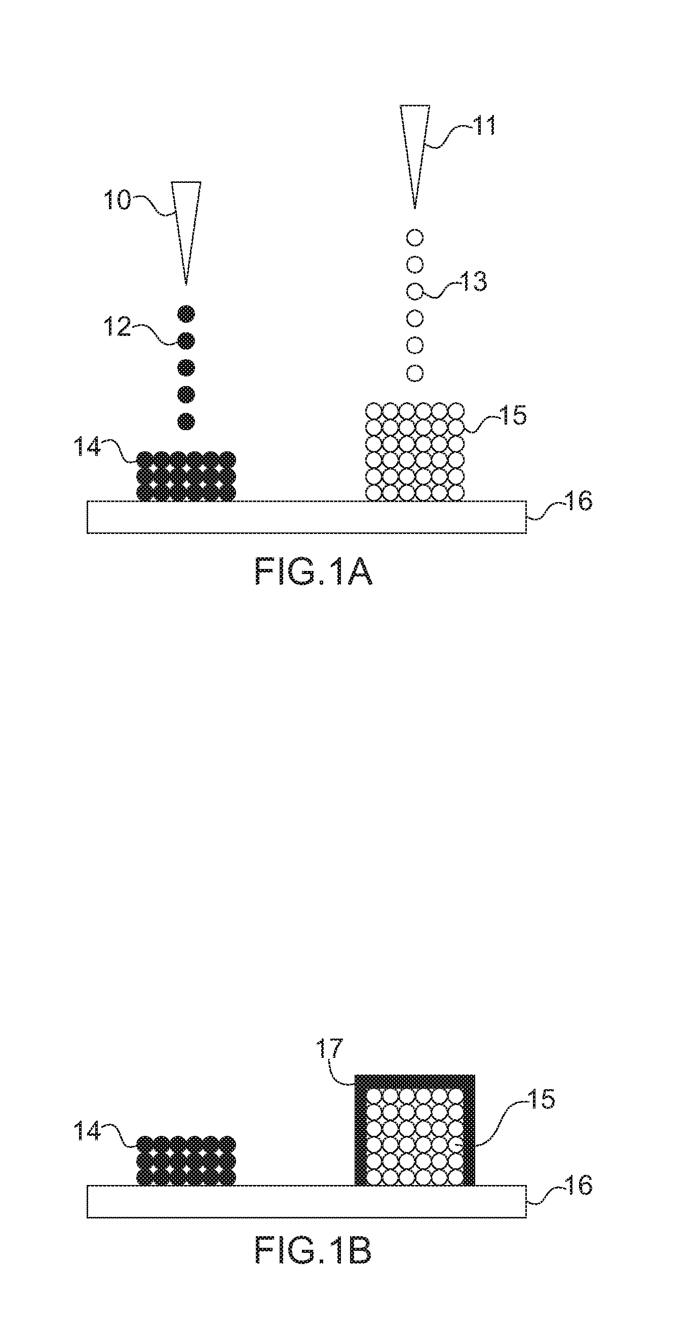
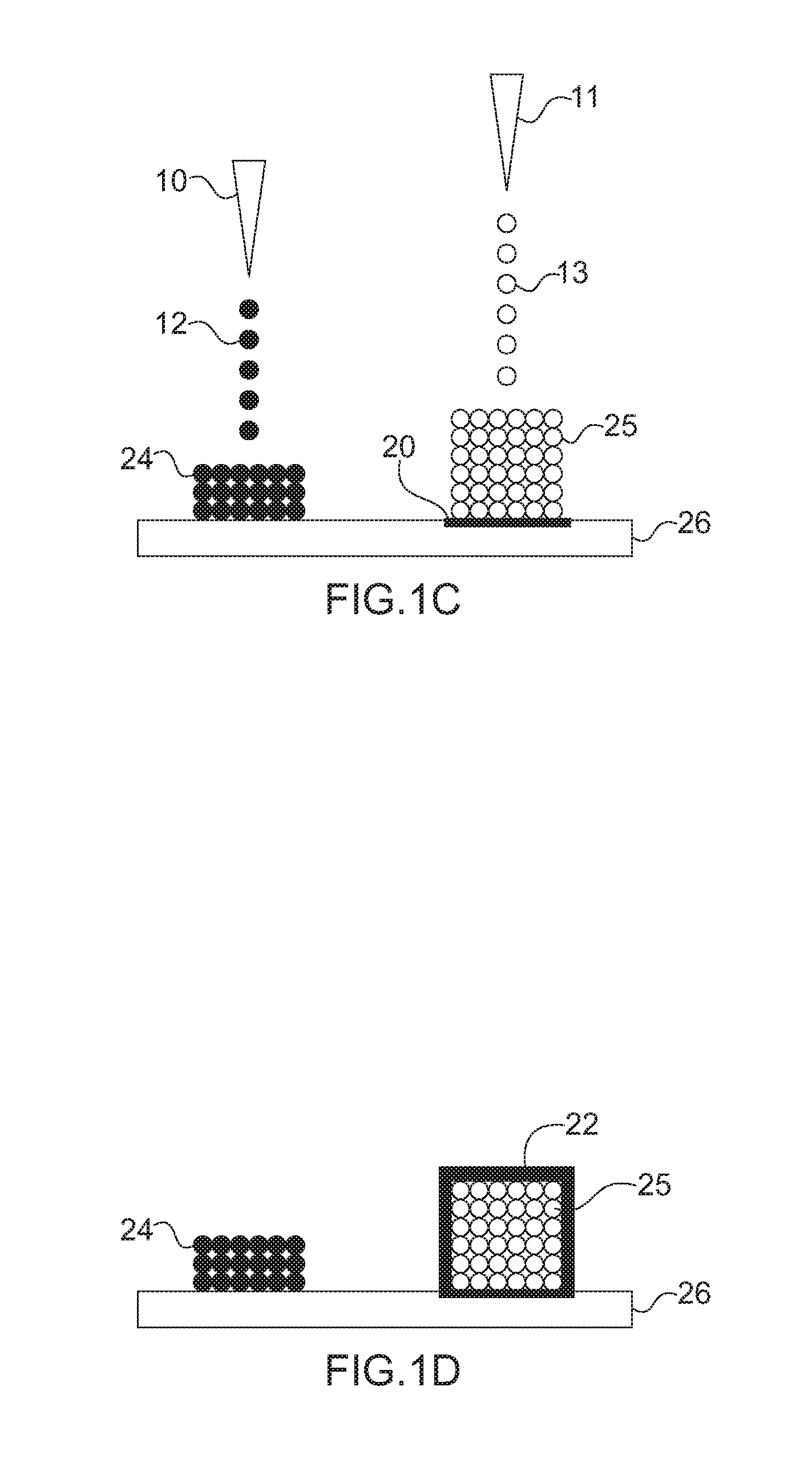
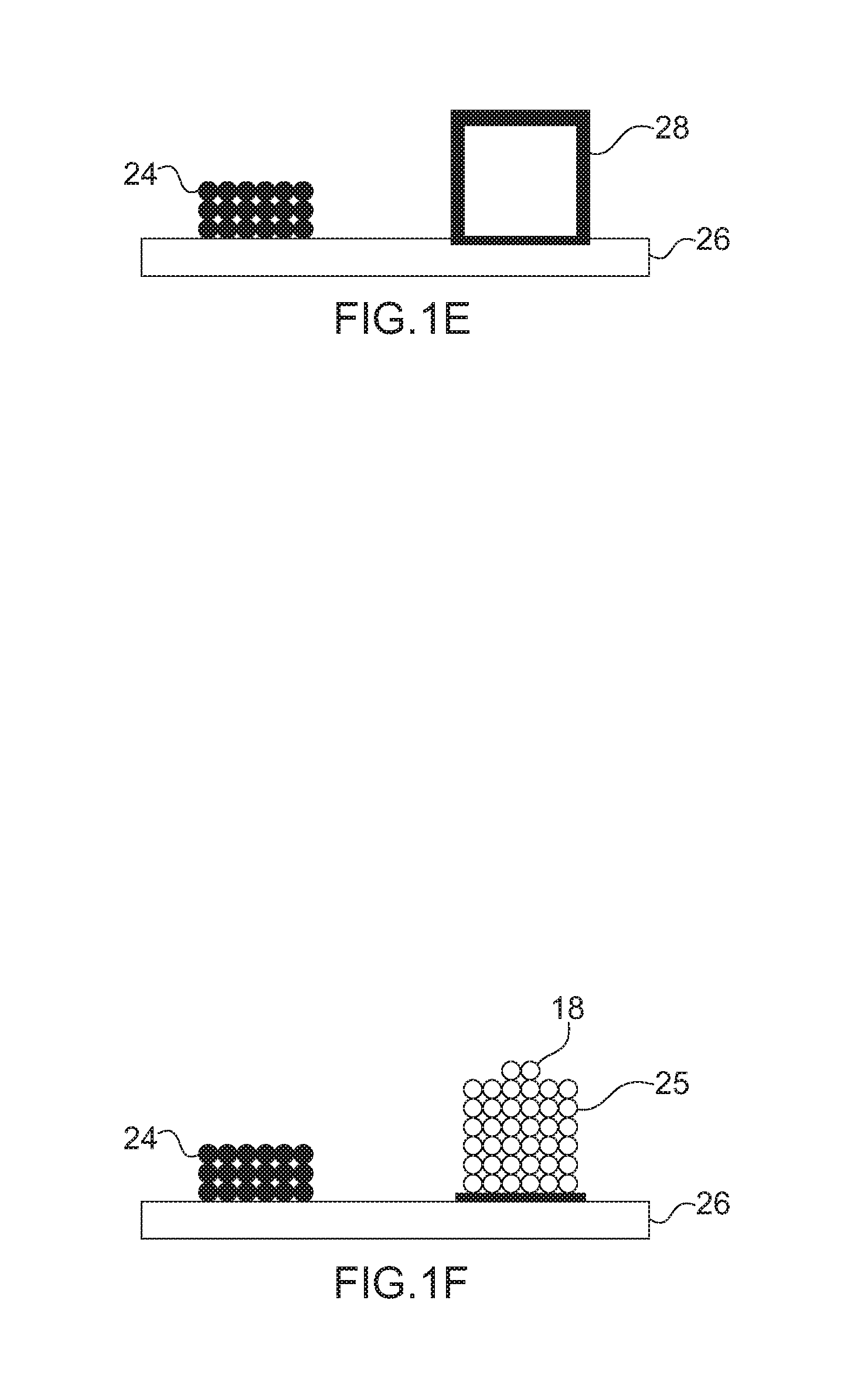
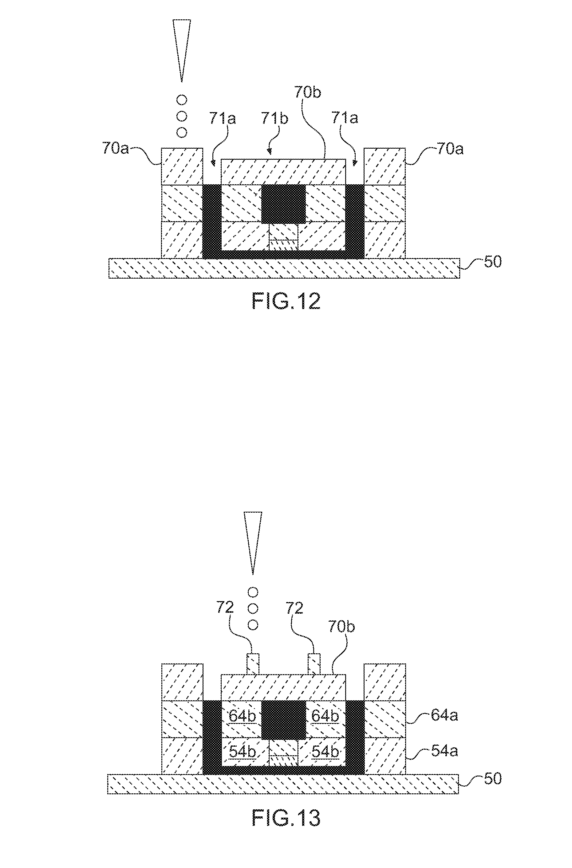
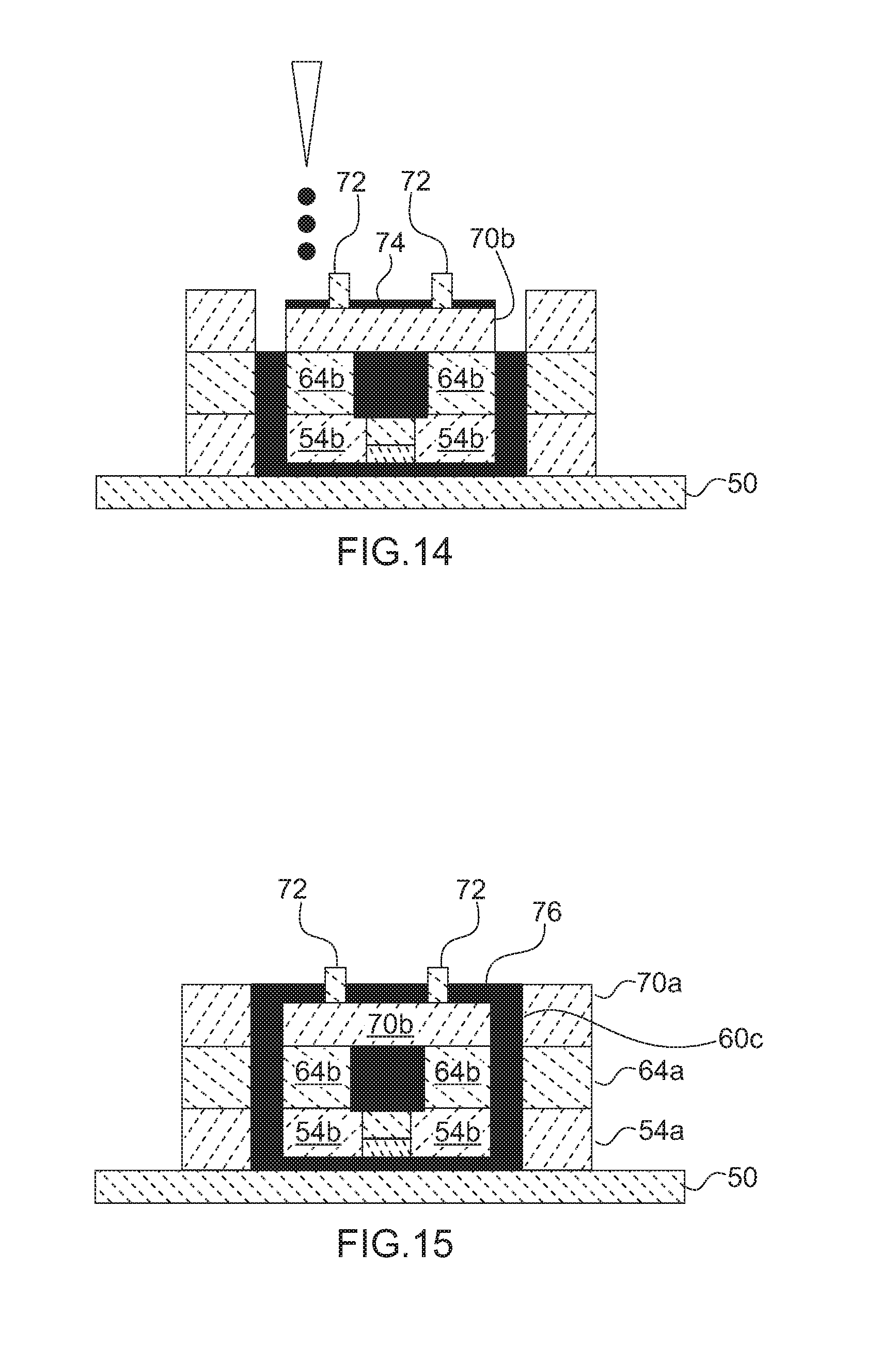
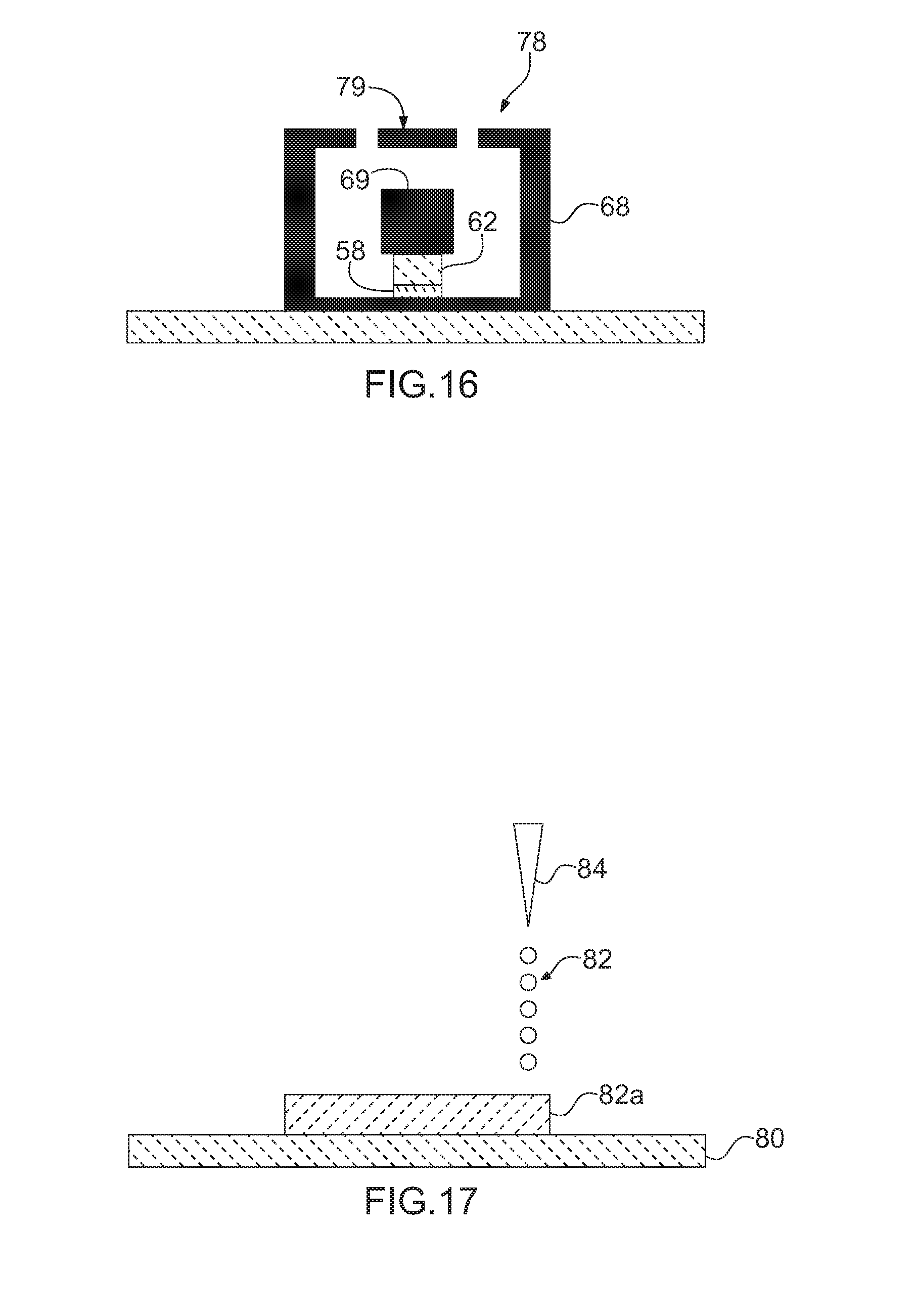
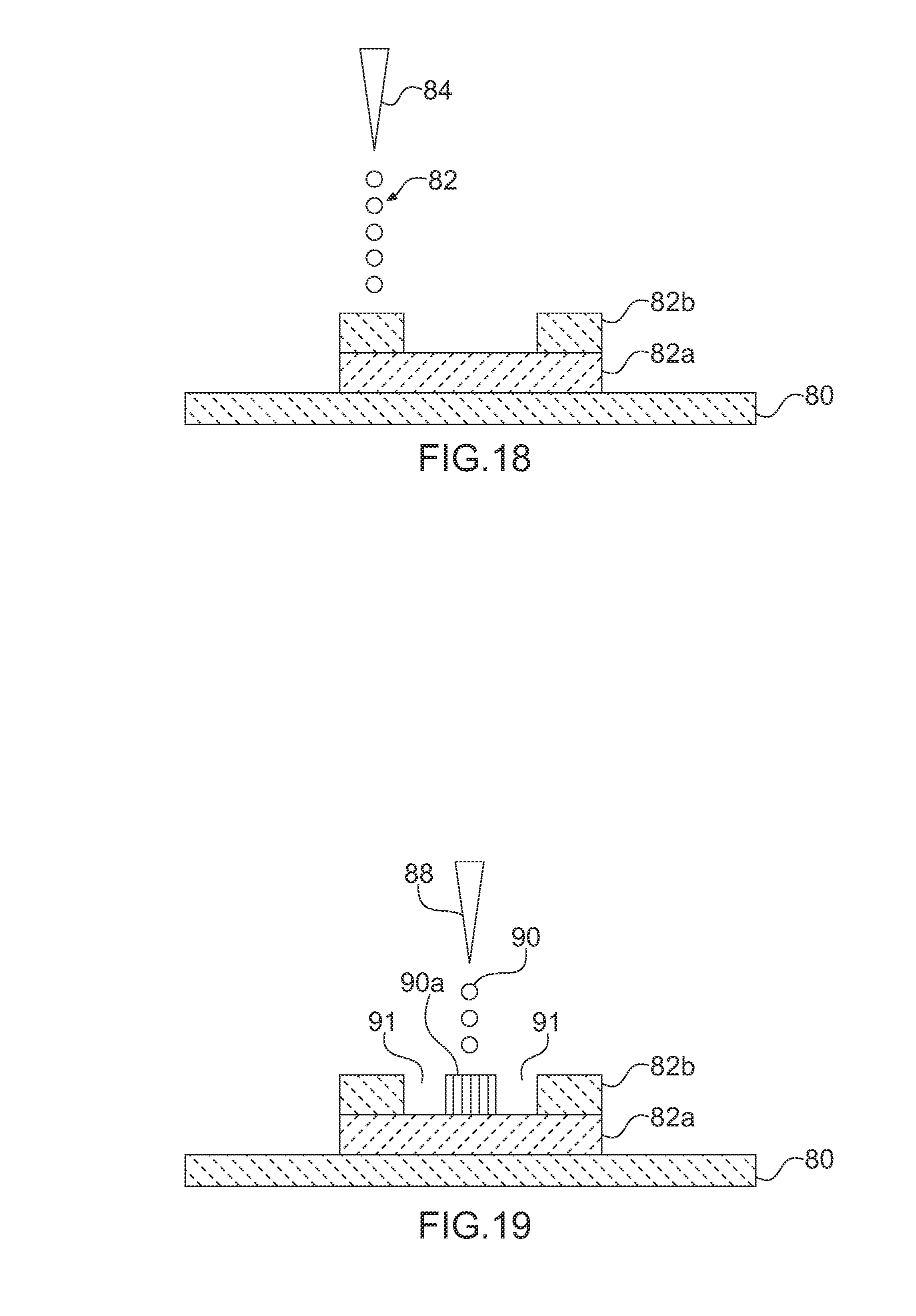
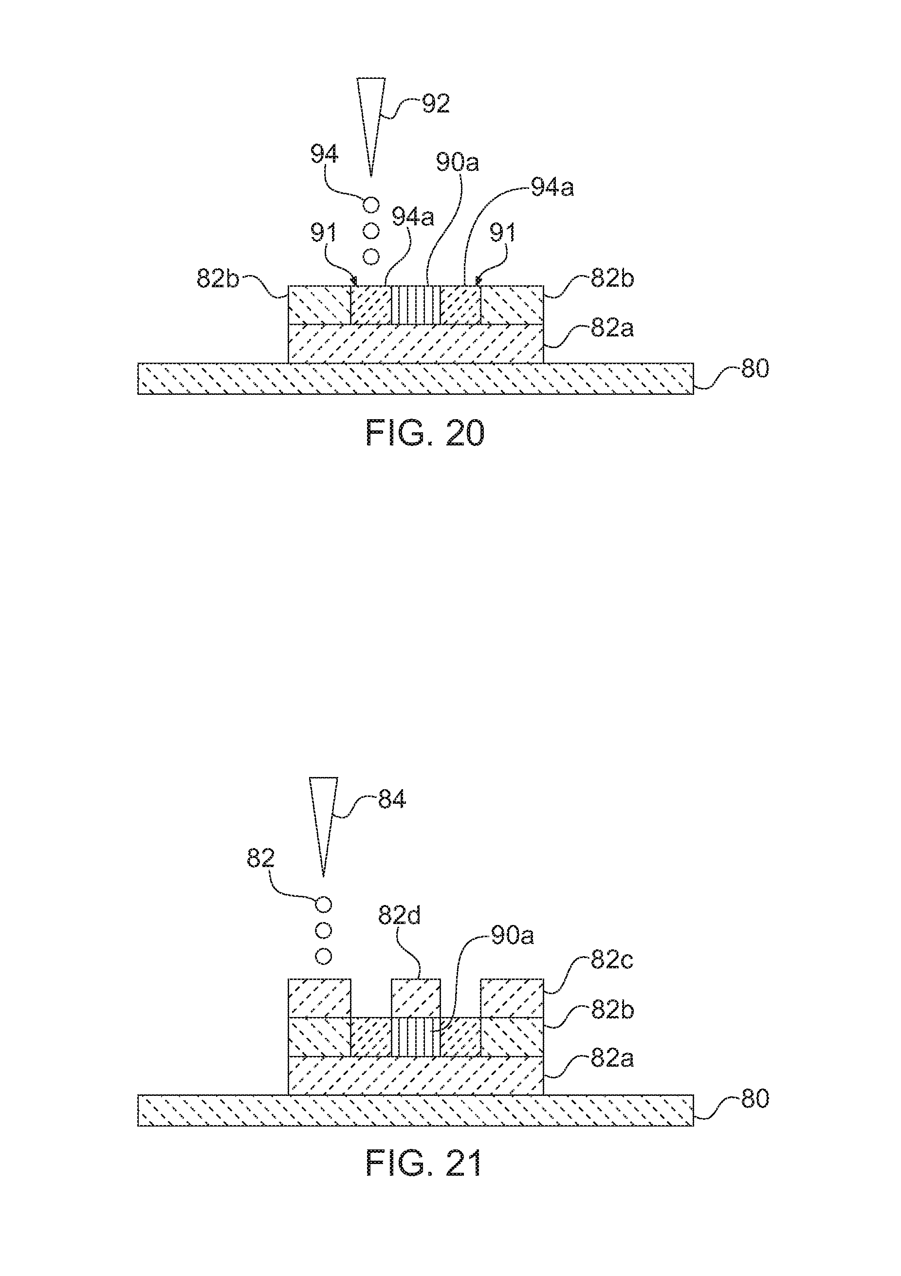
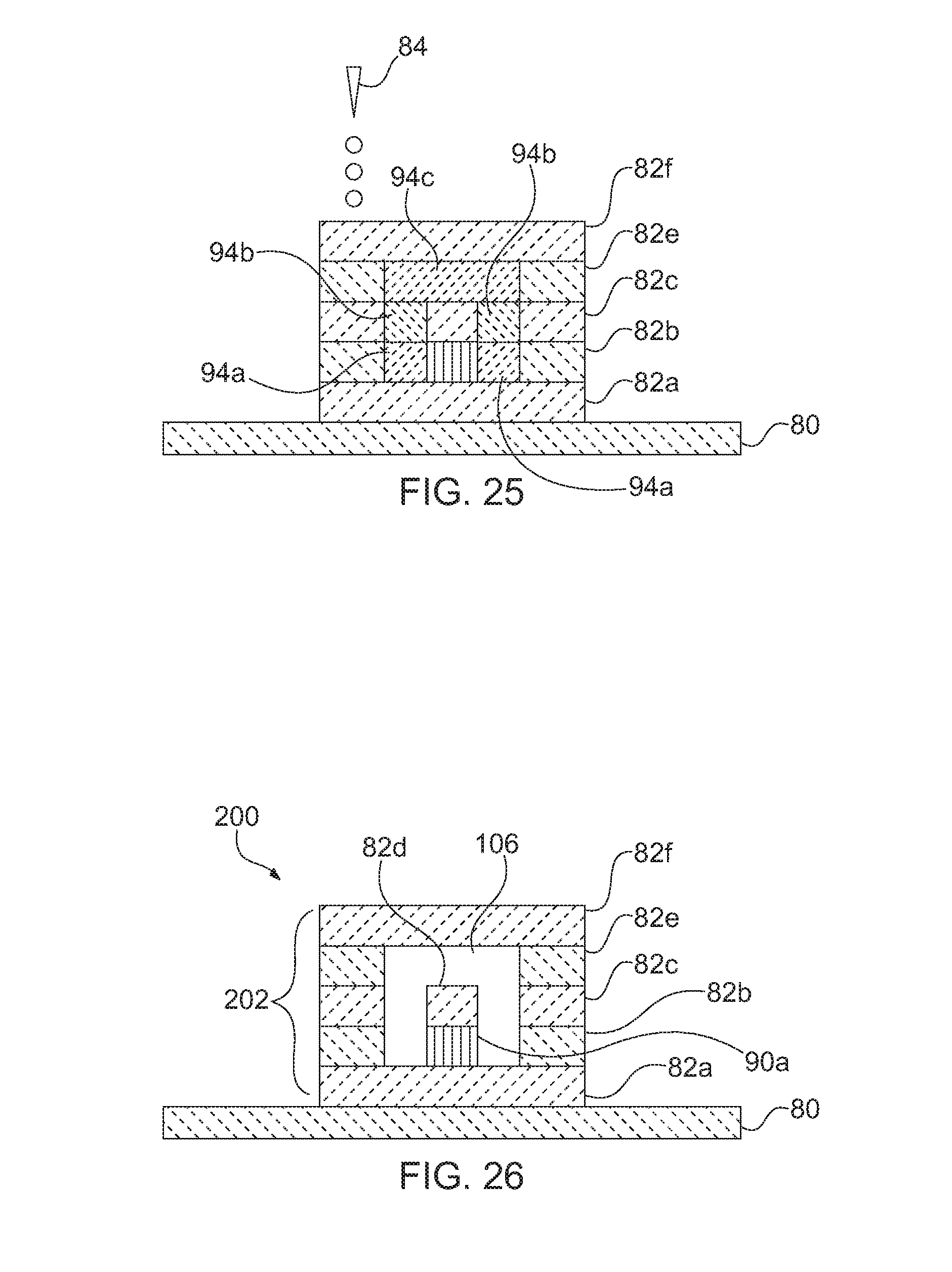
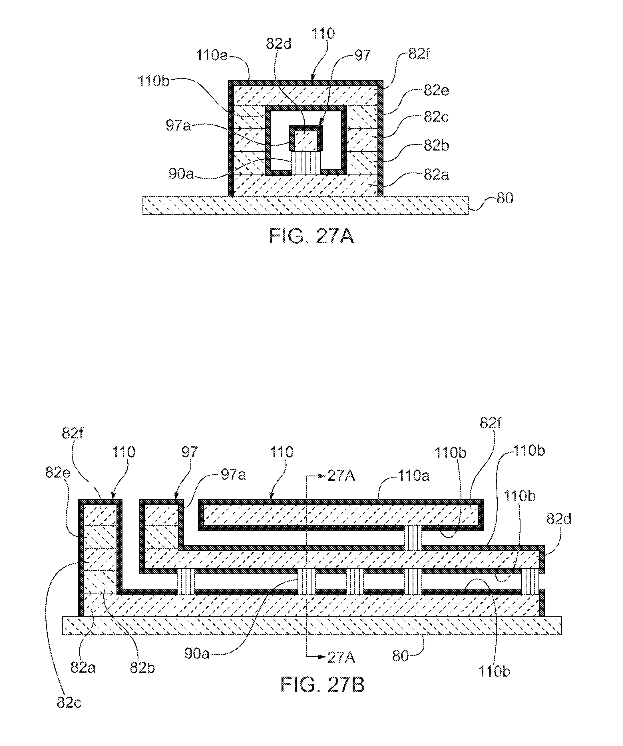
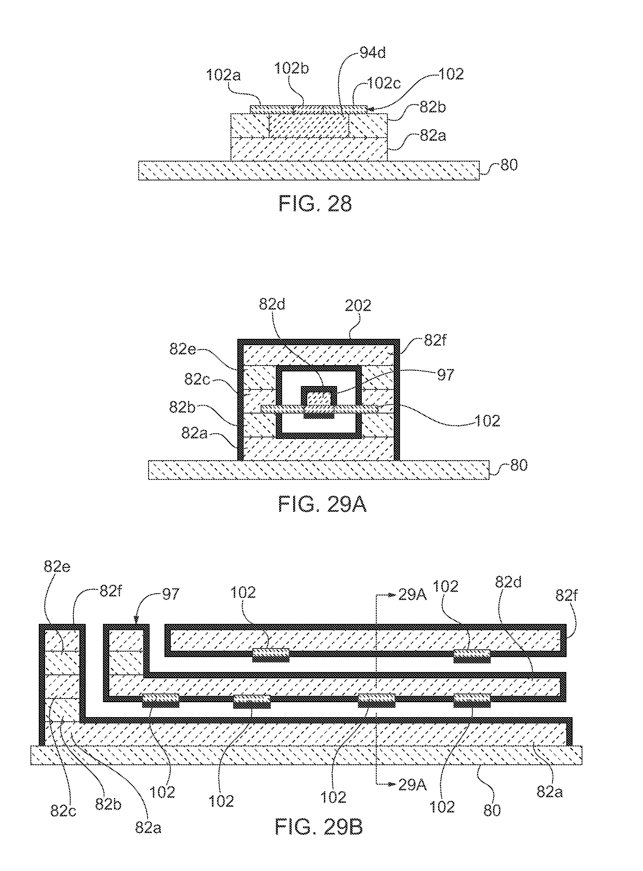
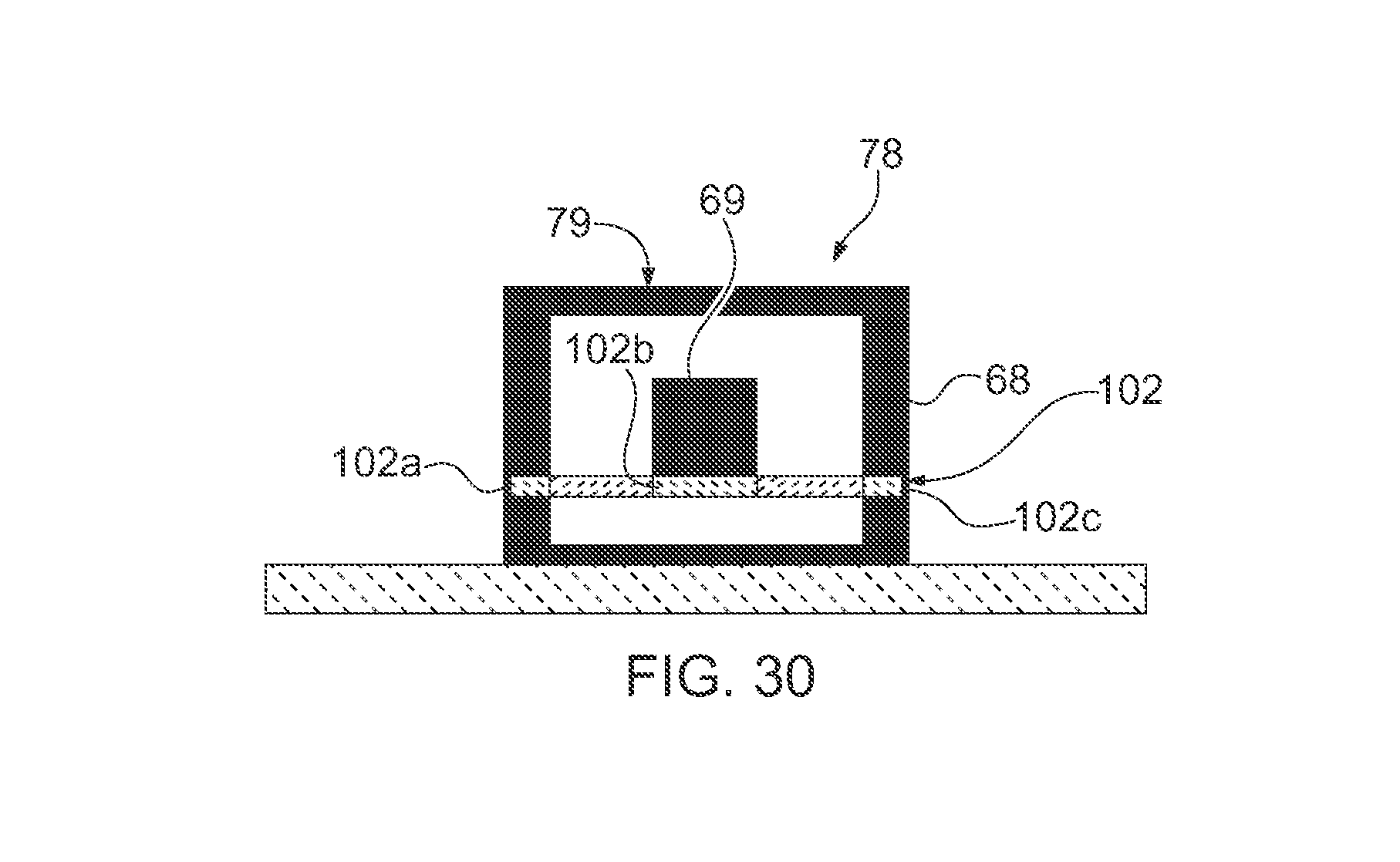
This application is a continuation of U.S. application Ser. No. 14/232,396, filed Jan. 13, 2014, now U.S. Pat. No. 9,993,982, which in turn is a 371 application of International Application No. PCT/US2012/046734 filed Jul. 12, 2012, which claims priority to U.S. Provisional Application No. 61/507,496 filed Jul. 13, 2011. Each of the foregoing applications is hereby incorporated herein by reference. The present invention relates to the fabrication of electronic and/or mechanical structures and components and devices such as those used in the electronics industry. In particular, the present invention relates to using homogeneous or heterogeneous materials in three dimensional fabrication of electronic and/or mechanical structures and components and devices. Additionally, the present invention relates to selective metallization processes including electroless and/or electrolytic metallization. Improved methods of fabricating electronic and/or mechanical structures continue to drive the electronics and other industries. More and more components are being added to devices that are getting increasingly complex and smaller. As a result fabrication techniques are required to provide electronic and/or mechanical components and/or parts that have increased functionality as well as to take up less space in the device and on substrates used in the device. The fields of micro-mechatronics, microsensors such as multi-axis gyroscopes, electrical circuits, and microwave and waveguide circuits are rapidly advancing. The ability to achieve customization in such devices and still allow them to be affordably manufactured has remained a challenge. Most industrial shaping, forming, and production processes achieve economy of scale only by near direct duplication of a device. For example, consumer electronics are affordable when making millions of complex integrated circuits that are nearly identical. Still there are many fields where the ability to make custom 3D parts of heterogeneous materials has remained elusive and substantial sacrifices in dimensional accuracy and precision, material diversity, upward or downward size scaling, for example from microns to meters, and/or other limitations have relegated most direct 3D manufacturing to either be unaffordable, impractical, or find limited fields of use, for example to make plastic prototypes for novelty, engineering understanding, or marketing. In micromechanics, processes to make small components often revolve around removal rather than additive processes such as turning or milling operations and such devices are typically made one at a time. Alternatively, molding is used but is limited in the complexity of the parts and number that can be made and are usually of limited material diversity. For example, one would not expect injection molding to make parts of plastic, metal, and ceramic in the same molding operation. Processes that have been created to address the fabrication of components and devices of very high precision and accuracy traditionally revolve around photolithographic processes and deposition and/or etching processes. For example, in traditional thin film metallization patterning for integrated circuits and circuit boards, temporary photoresists are patterned on metallic layers followed by etching of the exposed metal, then removed to leave a metallic pattern. Alternatively, metal can be plated into the exposed areas of the photoresist followed by removal of the photoresist and flash etching to leave behind a metallic pattern. Thicknesses of the patterns are limited to the thickness of the original metallic layer, in the case of etching, and the thickness of the photoresist, in the case of metallic plating. Current fabrication processes include, for example, permanent resists, generally known as photoimageable dielectrics (PID). It may desirable that such materials have low dielectric constants and low dielectric losses particularly when they are a permanent part of an electronic component and/or device. They are coated onto a substrate from either a liquid composition or by using a dry film, indiscriminately, coating the entire substrate. They can be used to photodefine structures wherein the PID can be cured to become a permanent part of the electronic and/or mechanical component and/or device. Adhesion promotion and catalyzation of the surfaces of the cured PID may allow for metal to be deposited onto the surfaces of the resist. In some processes, a temporary photoresist may be metallized or the resist may serve as a mold for the metallization; this is followed by removal of the resist leaving behind a metal structure with air as the dielectric. In addition, many structures require more than one layer of dielectric material and/or conductive materials such as, for example, metal. To create devices that have substantial complexity, tens, hundreds, or even millions of layers may be required depending on the size, scale, and resolution desired. Furthermore, the use of PIDs to create such devices is very limiting. After a layer of PID is imaged to form a structure, a second layer, uniformly applied from either a liquid or a dry film, has difficulty planarizing or filling the spaces in the structure particularly if they are on the scale of the layer's thickness or greater. A further limitation is the inability to create structures of varying and specific desired thicknesses since the PID can only be applied as one uniform thickness when applied by these methods. Still a further limitation is the inability of the PID to allow for selective metallization. Adhesion promotion and catalyzation of the PID surfaces is non-selective so that every exposed surface will be metallized, rather than a select set of surfaces. A still further limitation of the current techniques is the inability to create structures that differ substantially in size, functionality, and accuracy and also can provide the needed material diversity wherein the materials have both acceptable properties in comparison to other forming techniques currently known—for example finding a process that can provide the properties of metals, dielectrics, and some polymer materials that can be achieved through means such as thin film deposition, plating, sintering, and so on. Even without material diversity, the materials available in the 3D printing processes themselves often have compromised material properties compared to the material available in bulk or through other forming methods. This is particularly true when attempting to create multicomponent structures in the 3D printing process. For example, the properties of a 3D printed conductor or metallization may have unacceptably low electrical or thermal conductivity compared to a vacuum deposited or plated counterpart. For a dielectric such as a ceramic, or even a polymer composition, properties such as the dielectric constants, dielectric losses, and density may be unacceptably compromised. Thus, it may prove unacceptably challenging to obtain a suitable diversity of desirable materials, having a large enough set of desirable material properties, to create many functional devices that would be desired, for example, that which would desirably be associated with creating a 3D printed and fully functional version of many components populating an electronic and/or mechanical device. For instance, to create a circuit board, both a good electrical conductor and a good non conductor are required in a pattern. It may also be important in the final device that its metals or conductors are able to take a solder based device attachment; and that its adjacent non-conductors can withstand the temperatures associated with this process. Finding a 3D printing process that can provide metal properties found in plated metals and in the same process finding a dielectric that will both suitably adhere to said printed metal and have an acceptable decomposition temperature, chemical resistance, and other suitable dielectric properties can be difficult with the processes currently available in 3D printing. The current processes are of little use when a substrate has components or other elements already fabricated onto or into the substrate particularly where the topology is substantially non-planar with respect to the layer thickness. Also, many substrates are sensitive to the solvents or heating steps that are required in fabrication. Alternative methods of preparing these devices with many components include molds and pick and place processes wherein the components are made “off-line” and are assembled later onto the electronic and/or mechanical device. Classic examples include capacitors and resistors, and inductors as well as magnetic components. As can be seen, current methods for the fabrication of electronic and mechanical structures for manufacturing electronic and/or mechanical components and other objects are limiting. Thus, there is a need for devices and methods of fabrication that allow electronic and/or mechanical structures to be made with varying sizes, thicknesses, and materials as well as the ability to be preferentially metallized—including devices and methods that can be utilized in a non-destructive manner when substrates are already populated with devices. In a first embodiment, the present application for patent discloses and claims a method of fabricating three dimensional electronic and/or mechanical structures by selectively depositing at least one dielectric material, which comprises a metallizable composition, using three dimensional printing methods and selectively depositing metal onto the metallizable dielectric material. The deposited dielectric material, which comprises a metallization composition, may further be made from a photoimageable composition and/or patterned using lithographic processes such as, for example, contact printing, projection printing, direct write printing, and/or other lithographic processes. In a second embodiment, the present application for patent discloses and claims a method of fabricating three dimensional electronic and/or mechanical structures by selectively depositing at least one dielectric material, which comprises a metallization composition, using three dimensional printing methods and depositing at least one dielectric material which does not comprise a metallization composition and selectively depositing a metal onto the metallizable dielectric material. In a third embodiment, the present application for patent discloses and claims a method of fabricating three dimensional electronic and/or mechanical structures as in either of the previous two embodiments but further comprising depositing a sacrificial material comprising a metallizable composition, selectively metallizing the sacrificial material and removing the sacrificial material. The sacrificial material may be comprised of a photoimageable material that can be lithographically imaged using lithographic processes such as, for example, contact printing, projection printing, direct write printing, and/or other lithographic processes. The removal of the sacrificial material may be performed by organic solvents, aqueous solvents and/or thermal vaporization and optionally may include mechanical assistance such as, for example, ultrasonification. In a further embodiment, the present application for patent discloses and claims a method of fabricating three dimensional electronic and/or mechanical structures by selectively depositing one dielectric material using three dimensional printing methods, selectively depositing a second dielectric material using three dimensional printing methods, selectively catalyzing one of the dielectric materials with a plating catalyst and selectively depositing metal onto the catalyzed dielectric materials. Either, or both, of the dielectric materials may be photoimageable and can be imaged using lithographic processes such as, for example, contact printing, projection printing, direct write printing, and/or other lithographic processes. In a further embodiment, the present application for patent discloses and claims a method of fabricating three dimensional electronic and/or mechanical structures of the immediately above embodiment, but further comprising depositing a sacrificial material comprising a metallizable composition, selectively metallizing the sacrificial material, and removing the sacrificial material. The sacrificial material may be comprised of a photoimageable material and can be imaged using lithographic processes such as, for example, contact printing, projection printing, direct write printing, and/or other lithographic processes. The removal of the sacrificial material may be performed by organic solvents, aqueous solvents and/or thermal vaporization and optionally may include mechanical assistance such as, for example, ultrasonification. In still a further embodiment, all of the above embodiments are deposited in a selected plurality of layers to give a sequential build of electronic and/or mechanical structures, wherein the layers comprise one or more of a metal material, a sacrificial material, and a dielectric material thereby forming a structure above the substrate. In the above embodiments, the three dimensional printing methods can be, for example, stereolithography, 2-photon stereolithography, inkjet, hot melt extrusion fabrication, and/or selective laser sintering. All of these embodiments and their variants may have in common the use of a dielectric that is selectively metallizable in conjunction and relation with a second dielectric to form mixed metal-dielectric structures and metal-dielectric-void structures. The foregoing summary and the following detailed description of the exemplary embodiments of the present invention may be further understood when read in conjunction with the appended drawings, in which: The present invention relates to processes and devices created, at least in part, utilizing three dimensional (3D) additive build manufacturing as a way to create 3D objects by going from a computer or digital design of the 3D object to the object itself from this digital information. In one of its aspects, the present invention relates to simple and complex electronic and/or mechanical structures and processes for their formation. In one notable aspect, the present invention relates to devices having conductive structures with tolerances and accuracy on the micron scale, such as microwave and waveguide circuits. In this regard, the present invention provides novel methods for creating such conductive structures via 3D additive build manufacturing while overcoming present difficulties in providing conductive structures of small dimension and high tolerance and having suitable bulk electrical and thermal conductivity properties made via 3D additive build manufacturing. In particular, the present invention may use selective metallization processes and materials in conjunction with non-conductive structure(s) provided by 3D additive build processes described below to provide micron scale accuracy conductive structures within a multi-structure and/or multi-component device environment, for example. As used herein, “selective metallization” connotes the ability for one material to take or bind to a metallization process or to a metallization catalyst with respect to a second material which does not so take or bind when both are exposed to the same metallization process. Thus, selective metallization permits selected structures to be metallized while other structures within the overall device/system architecture are not. A number of motivations for this selectivity have been discovered. One motivation is that some of the highest accuracy and tolerance 3D printing methods such as stereolithography tend to be formed from light solidified monomers or polymers. Even if one used electrically conductive polymers however, they are not typically able to provide bulk conductivity of a dense metal such as silver or copper. While it is possible to coat most plastic surfaces with a metal—for example by electroless plating—it is not possible to use current techniques with precision to choose where metal will and will not be coated except in the case of a planar and smooth exterior of sufficient dimensions, for example with additional masking. Thus, in accordance with the present invention the desirability of having a deposited material with near bulk-conductivity grow and adhere where desired, or through other means such as later stage thermal processing, is recognized. Turning to the different technologies available for performing additive manufacturing or 3D printing, 3D additive build manufacturing has come to include additive manufacturing methods such as Selective Laser Sintering (SLS), and StereoLithography (SLA), and micro-stereolithography. Other additive manufacturing methods include Laminated Object Manufacturing (LOM), Fused Deposition Modeling (FDM), and MultiJet Modeling (MJM), and Inkjet. Areas of substantial overlap can exist between many of these methods, which can be chosen as needed based on the materials, tolerances, size, quantity, accuracy, cost structure, critical dimensions, and other parameters defined by the requirements of the object or objects to be made. In addition, 3D additive build manufacturing has come to be known by a variety of names, including 3D printing, for example. Thus, as used herein the terms “3D additive build manufacturing” and “3D printing” are used interchangeably. Three dimensional (3D) printing is a form of additive fabrication or additive manufacturing technology wherein a 3D object is created by laying down or forming successive layers of material at precise positions. Thus inkjet, fused deposition, and multij et would all be forms of 3D printing. 3D printers have the ability to print structures made of several materials with different mechanical and/or physical properties in a single build process, and operate by taking a 3D computer file and constructing from it a series of cross-sections taken in the build direction. Each cross-section layer is then printed one on top of the other to create the 3D objects. (When the term “layer” is used herein, it means one or more levels or of potentially patterned strata and not necessarily a continuous plane.) Alternatively, a 3D printer can create a 3D object from an extrusion of a liquid that is solidified by either a change in temperature or a chemical change, for example, such as melting or polymerization. Thus, while a layer-wise build may be used in some instances, a vector-based build where 3D motions both in and out of a plane are determined based on the part to be made, machine physics, material chemistry, and other manufacturing considerations can also be used. In plane rastering and out of plane motion of a “print head” supplying a material, or for the same “print head”, adjusting the 3D coordinates of a critical focal volume of light within a photosensitive liquid and (thereby converting it in that location to a solid “voxel”) are both methods where, through motion and repetition, a 3D object of some target physical dimensions, shape, and size can be formed. A number of different technologies are available for performing 3D printing. Their main differences are in the way layers are built to create objects. Some methods use melting or reflow to produce the layers such as in “selective laser sintering” wherein one or more lasers selectively fuse particles from a bed of particles. After each cross-section is created, a new layer of powder is applied to the top and the processes repeated until a desired 3D structure is obtained. Depending on desired properties, each layer of powder may be the same, or a layer of different powder may be applied. Each powder layer may be uniform or the layer can be sectioned with differing materials, thus providing the capability of obtaining objects with differing characteristics and/or functionalities. This technique is also useful for producing fused plastic layers and/or plastic objects or metal layers and/or metal objects or ceramic layers and/or ceramic objects. For metallic structures, a bed of metallic powder is provided followed by exposure to a laser. For many functional objects in electronics and in mechanics, a combination of materials that include more than one of metal, ceramic, plastic, semiconductor, and others would be desirable. Thus it is desirable in such a process to control factors such as stress, shrinkage, CTE, material cohesion and inter-material interface adhesion in constructing or building such a 3D device of highly heterogeneous material types. Another method in additive manufacturing through 3D printing is “hot melt extrusion fabrication” wherein materials, supplied as pellets and/or a filament may be liquefied and deposited by one or more extrusion heads. The pellets and/or filaments may be the same or different and may be melted and mixed prior to or during extrusion. Other methods include application of liquid materials that are cured with different technologies, including inkjet printing. In the case of 3D structures, the “inkjet” may deposit layers, for example, from a micron to tens of microns or more in thickness in each layer. The layer may be cured as the process proceeds, for example, by drying. Alternatively, in one part, inkjet printing layers can be applied and cured one layer at a time. One or more printing heads, using similar or different materials, can be used to build structures on a substrate. Another inkjet printing technique is to inkjet a binder onto a bed of powder to bind the powder into a solid layer. The process continues until the desired 3D object is obtained. Another method of additive manufacturing using liquid materials is stereolithography wherein a vat or layer of liquid polymer is exposed to a light. The exposed regions of liquid polymer harden into solid layers. The substrate upon which the solid layer region was fabricated is then moved down in small increments and the liquid polymer is again exposed to light. The process repeats until the model is built. The liquid polymer is then drained from the vat, leaving the solid model. This method also allows for replacing the liquid polymer with a different liquid polymer at various stages during the building process, thus allowing for the use of different materials for different applications and with different properties. Other techniques include 2-photon stereolithography in which a 3D structure is obtained using one focused laser to create a 3D gel. This is followed by a second laser that cures the desired sections of the gel into a solid, with the uncured gel being washed away. Materials useful for the 3D fabrication of electronic and/or mechanical structures, include, but are not limited to, dielectric materials, for example, ABS, polyacrylates, BCB, polyimides, polyamides, polyurethanes, polyesters, polycarbonates, polysulfones, polysilicon materials and other materials known in the art to be useful as dielectric for fabrication of electronic and/or mechanical structures. While polymers may be most easily deposited materials using current 3D printing techniques, semiconductors, ceramics, and metals are typically found in electronic components. Selective laser sintering is one of the only additive manufacturing techniques that currently provides near bulk density metals, however its accuracy and resolution are low compared to jet deposited or extrusion deposited 3D printers. These materials however can be 3D printed as a mixture such as a nanomaterial paste or composition in a binder. 3D printing techniques that have a direct thermal component such as laser sintering can often provide a final structural material; however, other approaches such as baking the final printed structure to remove binders and certain polymer components could be equally used to obtain the final desired material properties. For instance, a polymer could be heat treated to remove solvent and leave behind a solid, or a polymer-ceramic composite could be heat treated to decompose the polymer and leave behind a ceramic. The materials may be used alone or may be formulated into inkjet compositions, or as meltable solids for hot melt extrusion application, or as monomeric, polymeric, or mixtures of materials for stereo-lithographic applications. Other useful materials may be applied by additive manufacturing or 3D printing processes and further processed in a curing step, for example, epoxy, novolac, melamine, glycidyl ethers of poly-bis-phenol A, or combinations thereof, and other crosslinking systems which require a thermal cure, a photo cure or a combination thereof. In some of these materials, one or more curing catalysts aid in the curing step, for example, photoacid generators, thermal acid generators, photobase generators and/or thermal base generators. Depending on the desired properties the materials for 3D printing may be combined into one or more useful printing compositions. In some embodiments, the compositions for 3D printing or additive manufacturing comprise a “metallizable composition”. These compositions may contain or may selectively bind to metallization catalysts, which allow for the deposition of metal using wet chemical processes or gas phase processes. Metallization catalysts include, for example, palladium-tin alloys which are activated to palladium catalyst during processing. Other catalysts include organic palladium materials which may be activated to palladium catalyst by thermal or chemical or plasma treatment. In some cases, a metallization precursor may be included in the dielectric being deposited. In some cases a material is chosen that can readily adsorb or absorb or bind to a catalyst from a solution in relation to a second material that does not absorb or adsorb or bind to the catalyst. In this embodiment, the material is deposited, the material may optionally be etched and may be optionally exposed to an additional step to concentrate the catalyst such as a plasma etching step that selectively removes a small amount of the polymer or binder material and leaves the catalyst. Further processing needed to activate a catalyst such as a palladium chloride composition, like exposure to a reducing agent, is known in the art. The material can then be plated. In other embodiments, the printing compositions may comprise photoimageable materials. For example, a photodefinable dielectric material, for example, glycidyl ethers of poly-bis-phenol A/photoacid generator systems, can be applied by 3D methods followed by further processing using photolithographic techniques such as, for example, exposing the material to actinic radiation through a photomask and removing any unexposed material using a suitable developer solution. This method could allow a two-fold patterning process, the first being the pattern provided by the 3D deposition, the second being a photolithographic process, and may provide more versatility in manufacturing a 3D structure. Other photolithographic materials may also be used for example, acrylate systems, BCB systems, silicon based systems and/or novolac systems. Using, for example, electroless metallization processes known in the art, metal may selectively be deposited, for example, copper, nickel, gold, tin, zinc, silver, palladium, tin, lead, aluminum, chromium and/or alloys. In some embodiments, the composition containing the metallization catalyst has its surface etched back to remove some of the non-catalytic dielectric material, thereby increasing the number of catalyst sites in the surface of the composition potentially allowing for improved plating. For example, etching steps to concentrate catalysts on a surface of the metallizable plastic may include plasma processes such as, for example, plasma etching in the presence of oxygen or may include wet chemical etching. Other dielectric materials not containing metal catalysts may be deposited along with catalyzed dielectrics. These can be deposited at the same time when using inkjet or hot melt extrusion printing by employing more than one printing head and/or sequentially such as, for example, with stereolithography where in one material is deposited from a liquid composition, the composition flushed and replaced by a second liquid composition which is then deposited. This allows for selective metallization wherein selected structures are metallized while other structures are not. To date, entire 3D printed plastic models have been metalized using plating on plastic techniques such as electroless plating and/or electroless plating followed by electrolytic plating; however, methods to selectively enable the formation of metalized regions along with non-metalized regions wherein the regions that become metal are defined by the materials deposited have not been demonstrated. This is in contrast with a patterned metallization in which an additional masking material such a resist or paint is applied to the object to create a metal pattern. In other embodiments, two dielectric compositions may be deposited onto a substrate using 3D printing methods, wherein only one of the dielectric compositions can be catalyzed with a plating catalyst and subsequently plated and the other does not take to or have the catalyst incorporated and so does not plate in the same metallization process. One way this can be achieved when one of the dielectric compositions has surface characteristics that allow a plating catalyst to adhere to it, while the other dielectric composition does not allow the catalyst to adhere. Examples of such adherent surfaces include surfaces with, for example, carboxylic acid, hydroxy and/or other highly polar groups on the surface and/or the surface may be porous allowing catalyst to be captured in the pores. Alternatively, one of the dielectric compositions may be treated with conventional plating on plastic processes, for example, slight swelling and etching of the dielectric followed by contact with a catalyst bath where the catalyst becomes adherent to the dielectric. The treated dielectric then is plated in a plating bath. The other deposited dielectric is selected such that it is not affected by the catalyzing and therefore the plating processes. Plating of the selected dielectric may be performed for example by electroless plating processes and/or by a combination of electroless plating followed by electrolytic plating, for example. In the above plating processes, it can be seen that the embodiments of the current disclosure provide for select plating and non-plating of the deposited 3D structure. The selective metallization may also occur by a gas or vapor phase reaction, for example in atomic layer deposition (ALD), a polar material may allow a series of gas phase reactions that metalize a surface were as a non-polar material may not start a reaction. In addition to 3D printing or additive manufacturing of permanent dielectric materials, metallizable or otherwise, the present invention includes the 3D printing of sacrificial materials along with one or more of the metallizable dielectric and the non-metallizable dielectric. For example, the 3D printed materials may be used to provide both a sacrificial scaffolding, for example, a starch, and a permanent material, for example, ABS. In this case, the final object is obtained when the sacrificial scaffolding is dissolved or otherwise removed. While parts entirely made of dielectric materials are useful in certain applications, other products, especially electronic and/or mechanical structures, benefit from having a mixture of metal and dielectrics available which may be combined with nearly arbitrary complexity, particularly when combined with a sacrificial material that can provide a space or void where desired. Thus typically three materials may be used, a sacrificial scaffolding material that can be dissolved after printing, and two materials one selectively metallizable in reference to the second, which remain intact during the process which removes the sacrificial scaffolding material. Subsequently, the metallizable material may be metallized during a metallization step, after which the selectively metallized material may optionally be removed in a second removal step. If the material is optionally removed, it may be desirable to ensure the metal is deposited to a thickness such that it can be free-standing. In some cases it may be desirable to have a dielectric, a metal, and a void structured in arbitrary and determined complexity in the final structure. Merely coating a dielectric, such as a selectively metallizable plastic, with a metal coating may not be desirable. A metal encapsulated dielectric may for example fail under temperature cycles due to a mismatch between the metal and dielectric properties, and therefore one may prefer to remove the metallized dielectric from the metal coating, similar to the removal of sacrificial materials that can serve as scaffolding. Thus one may choose 3 or 4 materials to realize such a device: a selectively metallizable dielectric, a second dielectric that does not become metallized in the same process, the metal that becomes coated on the metallizable dielectric, and optionally a scaffolding material. Typically, the scaffolding material is removed, then metal is deposited selectively on one of the two dielectric materials, and then the metallized dielectric material may also be optionally removed by a final removal process, leaving a desired metal, air, dielectric structure. Materials suitable as sacrificial materials can be printed using 3D techniques. Such materials are platable using the techniques described above, that is, they contain plating catalysts and/or can be swell/etched/catalyzed, and/or can be readily removed to leave behind a full or partial metallic structural element. Such materials include, for example, polyacrylates, polycarbonates, cellulosic materials, and other materials capable of being removed by a remover. Removers include organic solvents, for example, glycol ethers, glycol ether acetates, alcohols, esters, ethers, ketones, halogenated solvents, DMF, DMSO and the like; aqueous solvents such as acids and bases ranging in pH from about 0 to about 13 with or without surfactants and/or emulsifiers; and/or thermal vaporization, and/or combinations thereof. The sacrificial materials may dissolve, emulsify, particulate, depolymerize, and/or become gaseous. Additionally, mechanical assistance, for example ultrasonification, may also be used. The selectivity of the removers and the removal process require that the dielectric materials are not affected during the removal process. The current application also discloses depositing metalizable dielectrics, non-metalizable dielectric materials and sacrificial materials in a plurality of layers. The versatility of 3D printing allows a deposition of a variety of sequences of layers based on the electronic and/or mechanical structural requirements. For example, 3D-MERFS and PolyStrata®-like devices can be prepared by the disclosed methods. See U.S. Pat. No. 7,012,489, U.S. Pat. No. 7,649,432, U.S. Pat. No. 7,948,335, U.S. Pat. No. 7,148,772, U.S. Pat. No. 7,405,638, U.S. Pat. No. 7,656,256, U.S. Pat. No. 7,755,174, U.S. Pat. No. 7,898,356, U.S. Pat. No. 8,031,037, US 2008/0199656 and US2011/0123783, 2010/0296252, 2011/0273241, 2011/0181376, 2011/0210807 for examples of devices that can be prepared using the currently disclosed methods, the contents of which patents and published applications are incorporated herein by reference. In some embodiments, materials can be mixed in a reservoir prior to the printing of the material. This is particularly useful for materials that are highly reactive so that two materials may start to react with each other as they are being printed. In this manner, viscosity can build up quickly to help form a solid layer when the layer is applied. Two printing devices may work in concert with each other so that two parts of highly reactive materials can be printed simultaneously and begin reacting immediately, such as, for example, an epoxy novolac layer is printed from one printing device and an acid is printed by a second printing device directly onto the epoxy novolac layer. As soon as the acid comes into contact with the epoxy, a crosslinking reaction occurs. In other processes, some layers can be cured by heat and/or light, so that some of the printing heads can be replaced by or used in conjunction with heating elements and/or light emitting elements which may be applied to a layer which has been deposited. In this manner, the layers may be selectively cured or allowed to remain uncured, suitable for further processing. The electronic and/or mechanical structure may be deposited on a variety of different surfaces since the process is not dependent on coating processes that are typically required. Thus, a planar or nonplanar surface may be used to deposit the layers. Surfaces which are partially or fully populated with electronic devices and/or components may also be used and fabrication can take place on these surfaces, which is difficult to achieve with current conventional methods. The method for building electronic and/or mechanical structures may include depositing materials using conventional deposition processes, including, for example, spin coating, lamination, dip coating, curtain coating, slot coating, spray coating, off-set coating and the like. It may be desirable to planarize the structures after every layer or periodically, or provide selective removal steps during the processing of one or more layers. To that end, other conventional processes may also be included, for example, chemical-mechanical-polishing, lapping, mechanical machining, diamond turning or other precision turning, milling, grinding, plasma etching, laser ablation, and/or combinations thereof. The 3D printing process can provide structures of different shapes and/or different heights, as well as structures that have cavities and/or walls into which discrete components may be placed later during manufacturing. The current application for patent is not restricted to size such that objects from microns to meters can be fabricated using these methods and is primarily only limited by the resolution capabilities of the print head or the scale of the printer. Additionally, the substrate used for deposition may function only as a support onto which the objects, and all its embodiments, are printed, such that the substrate may later be removed providing a stand-alone object with selectively metallized portions on the object. Turning now to The printing heads 10, 11 may deposit layer upon layer until a desired thickness of structure is obtained. In some processes, the printing heads 10, 11 may provide multiple materials by switching from one material to another during the process, and differing ones of the multiple materials may be printed over each other to provide complex patterns. When layers are printed over each other, openings may be left in the layers to allow solution flow into and out of the structure formed of the layers. The substrate 16 may comprise any surface useful in forming an electronic and/or mechanical device including, for example, silicon materials, ceramic materials, glass materials, metal materials, integrated circuit containing semiconductor materials, circuit board materials, RFID substrates and the like. It may for example be a SiGe or InP wafer containing integrated circuits. The substrate 16 may be flat or, because of the versatility of the process, may be populated with components and/or structures that are already resident on the substrate 16. The substrate 16 may be a permanent part of the end product or it may be a temporary platform on which the structures are grown and/or removed and/or detached using, for example, a sacrificial layer. Alternatively or additionally, one of the materials, e.g., material 13, may contain plating catalysts. The catalysts may include one or more of palladium/tin colloid and/or their chloride salts, for example. After the printing process is complete (e.g., Turning to a further exemplary structure and method of the present invention, As mentioned, materials which are suitable for depositing can range from dielectric materials such as, for example, polyimides, polysulphones, polysilanes, and the like, as well as polyacrylates. Depending on the desired structure of the fabricated electronic and/or mechanical device, temporary materials may also be used such as, for example, waxes, solvent soluble materials and/or aqueous solution soluble materials. These materials can be important when the final fabricated device has air gaps or voids as shown in Turning now to A substrate 50 is provided having the bottom metallic wall 52 of the coaxial waveguide conductor cable 78 disposed thereon, A support post 62 may be deposited by inkjet printing a non-conductive material 63, such as any of the above mentioned dielectric materials, over the passivation layer 58 to provide support for the central conductor 69 of the coax cable 78, Optionally, while material 62 in Resuming the coaxial build example, sacrificial material 64 Sacrificial material 70 Dissolution plugs 72 may optionally be deposited via inkjet printing at selected location(s) on the surface of the sacrificial material 70 It should be noted that all the coating steps in this exemplary process were 3D additive build processes. Moreover, while plating was used as a method to obtain near bulk metallic properties in the 3D build, one or more of the plating steps could be replaced by a 3D printing step if suitable material properties needed can be obtained. Alternatively or additionally, as illustrated in the following example, conductive structures may be provided via metallization of selected non-conducting structures to yield solid or hollow structures having conductive surfaces as an alternative to structures with bulk electrical and/or thermal conductivity. Turning to A sacrificial scaffolding material 94 may be deposited through a deposition device 92, which may be the same or different than the deposition devices 84, 88, to selectively fill one or more of the voids 91 to provide a scaffolding 94 Returning to the build process, the deposition device 84 may next deposit a third layer of material 82 comprising structures 82 An upper structure 82 At this stage in the process the coaxial structure 200 may be nonconducting in view of the choice of materials 82, 90 utilized in the 3D additive build process, with layers 82 The metal coatings 97 In addition, during the sequential build multiple support posts 90 For example, the exemplary 3D additive build process may be altered beginning at the step of Optional release holes may be provided in closed structures or those that have limited flow to facilitate removal of the scaffolding 94 In addition, it should be clear that while a substrate 80 is used in the sequence illustrated in These and other advantages of the present invention will be apparent to those skilled in the art from the foregoing specification. For example, the build process outlined may contain more or fewer layers and more or fewer materials depending on the end device and/or structure being made. The build process could be stopped at any point and items or other materials maybe inserted into the partially complete structure and the build process then continued to embed and/or interconnect the inserted materials and/or devices. For example, passive or active electronic devices, magnets, powders, liquids and/or such may be put into cavities or receptacles and the build process continued to partially or fully interconnect or encapsulate them. Accordingly, it will be recognized by those skilled in the art that changes or modifications may be made to the above-described embodiments without departing from the broad inventive concepts of the invention. It should therefore be understood that this invention is not limited to the particular embodiments described herein, but is intended to include all changes and modifications that are within the scope and spirit of the invention as set forth in the claims. The present invention relates to the fabrication of complicated electronic and/or mechanical structures and devices and components using homogeneous or heterogeneous 3D additive build processes. In particular the invention relates to selective metallization processes including electroless and/or electrolytic metallization. 1-20. (canceled) 21. A method of fabricating a 3D structure, comprising:
providing a substrate having at least one integrated circuit disposed thereon; depositing onto the substrate using 3D printing a first dielectric material to create a first patterned layer having at least one region in which the first dielectric material is deposited and at least one void region in which no first dielectric material is deposited; depositing, on the first patterned layer, a second dielectric material to create a second patterned layer having at least one region in which the second dielectric material is deposited and at least one void region in which no second dielectric material is deposited; and depositing a metal into selected portions of one or both of the at least one void regions of the first and second patterned layers, thereby providing a 3D structure. 22. The method of 23. The method of 24. The method of 25. The method of 26. The method of 27. The method of 28. The method of 29. The method of 30. The method of 31. The method of 32. The method of 33. The method of 34. The method of 35. The method of 36. The method of 37. The method of 38. The method of 39. The method of 40. The method of 41. The method of 42. The method of 43. The method of 44. A method of fabricating a 3D structure, comprising:
providing a substrate having at least one integrated circuit disposed thereon; depositing onto the substrate using 3D printing a first dielectric material to create a patterned layer having at least one region in which the first dielectric material is deposited and at least one void region in which no first dielectric material is deposited; depositing, on the first patterned layer, a second dielectric material different from the first dielectric material to create a second patterned layer having at least one region in which the second dielectric material is deposited and at least one void region in which no second dielectric material is deposited; and exposing the first and second dielectric materials with a process that selectively deposits metal on only one of the first and second dielectric materials.RELATED APPLICATIONS
FIELD OF THE INVENTION
BACKGROUND OF THE INVENTION
SUMMARY OF THE INVENTION
BRIEF DESCRIPTION OF THE DRAWINGS
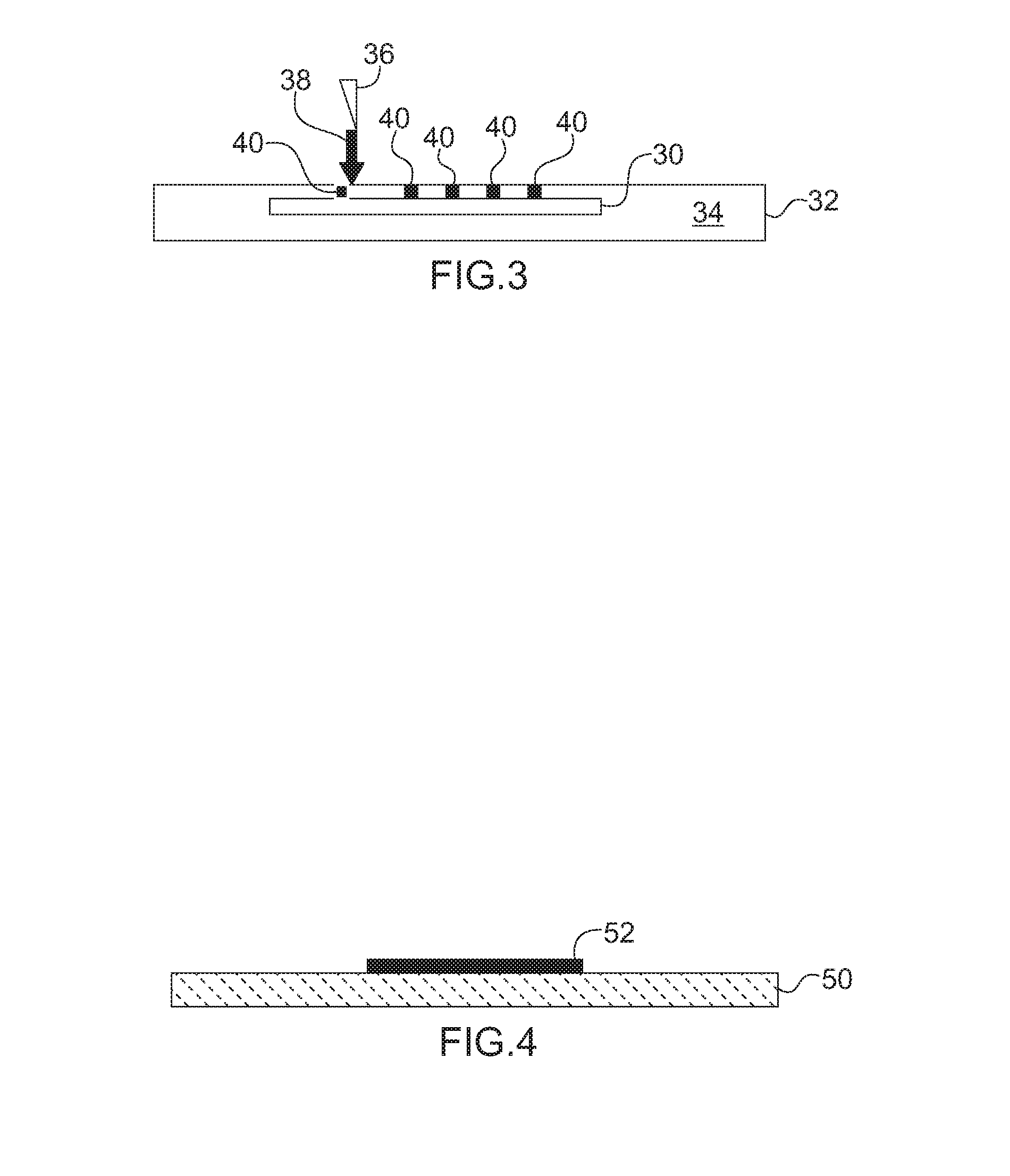
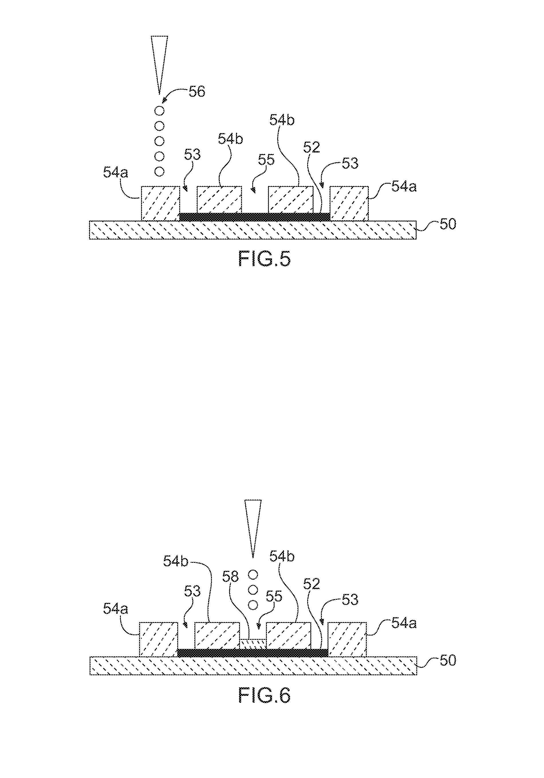
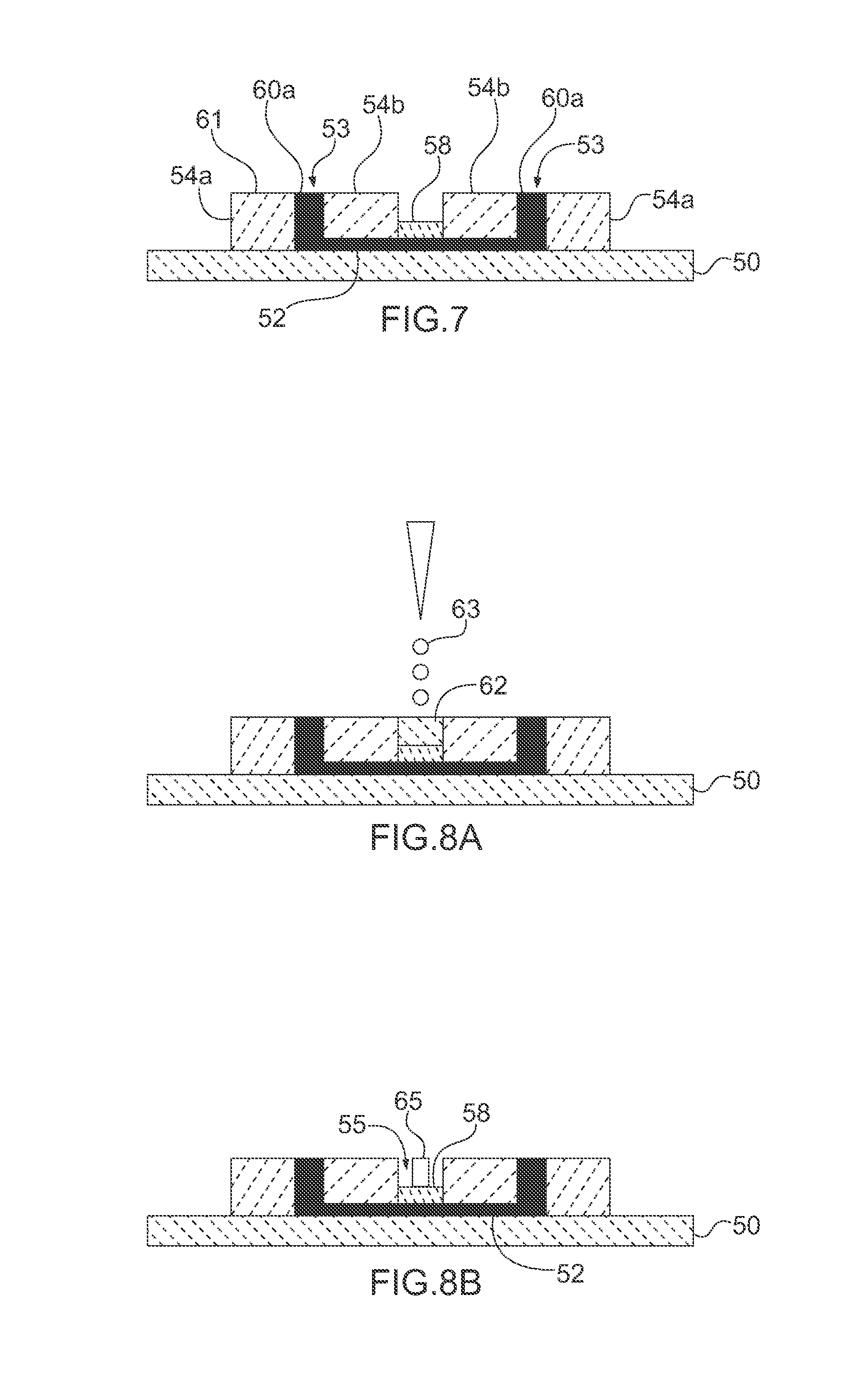
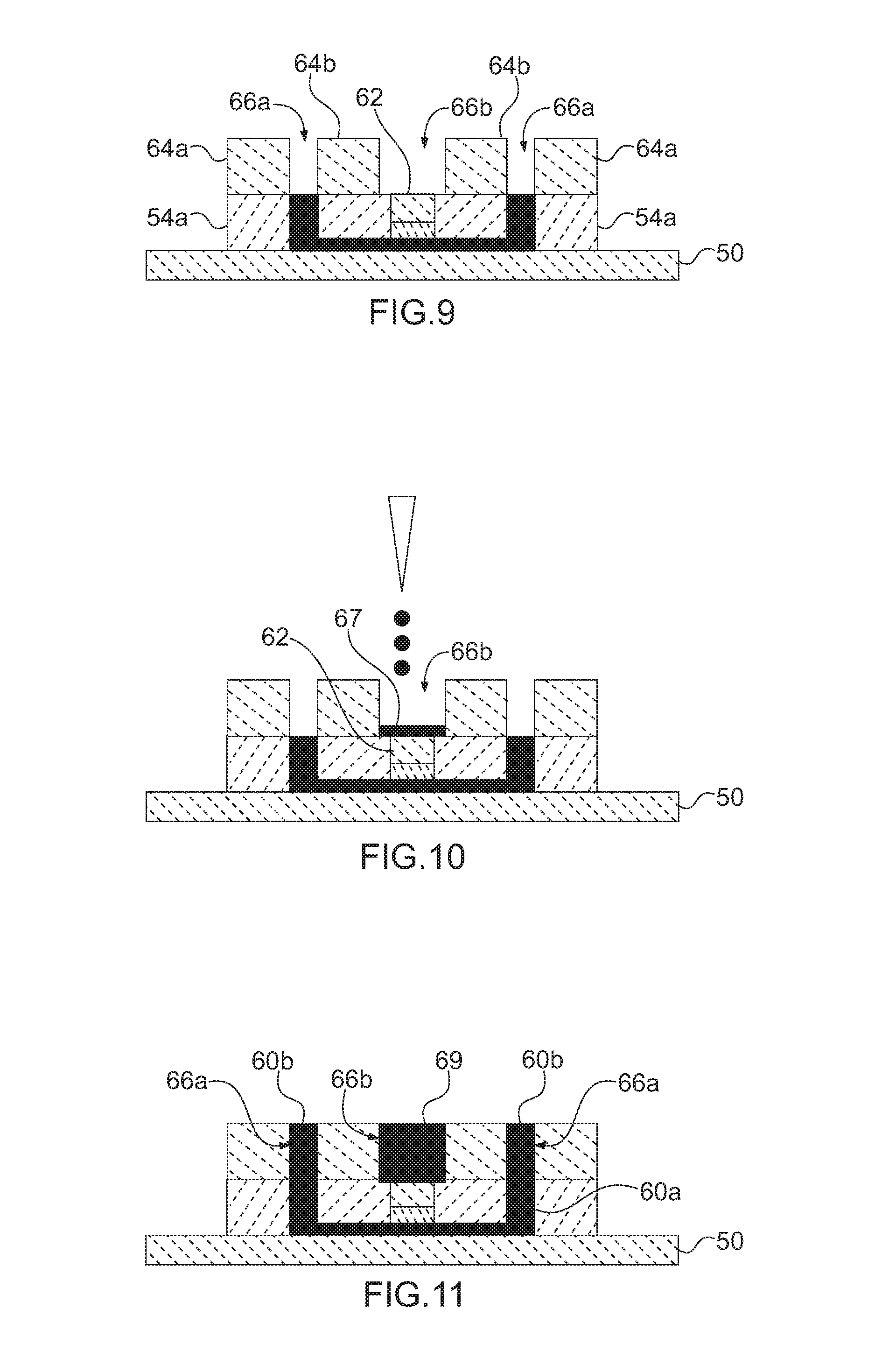
DETAILED DESCRIPTION OF THE INVENTION