Systems and Methods for Providing Multiple GPIO Supply Modes
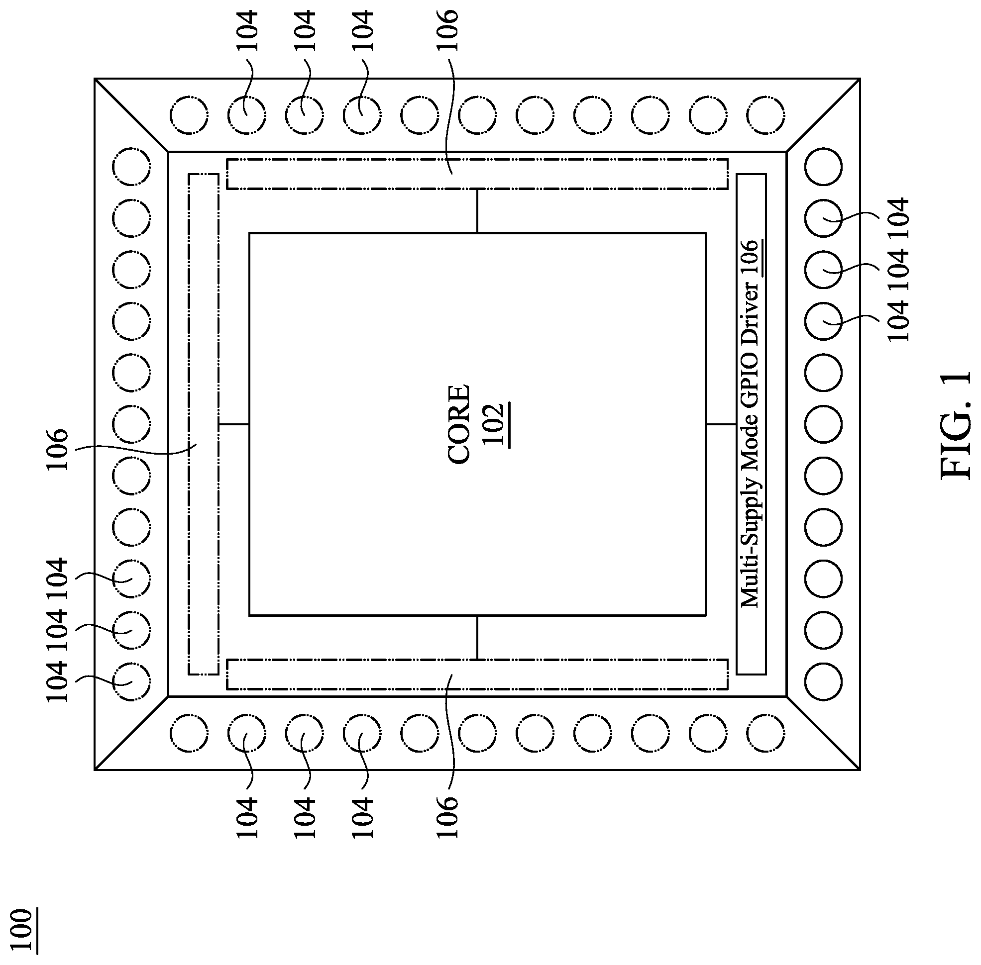
This application claims priority to U.S. Provisional Application No. 63/214,854, filed Jun. 25, 2021, which is incorporated herein by reference in its entirety. An integrated circuit may take the form of a set of electronic circuits embodied on a piece of semiconductor material, oftentimes silicon. In many implementations, the integrated circuit is designed to provide certain computing functions. In some instances those computing functions may be based on data or signals input to the integrated circuit from one or more sources external to the integrated circuit. In certain examples, the integrated circuit may further output data or signals that the integrated circuit generates based on its computing functions to destinations external to the integrated circuit. Aspects of the present disclosure are best understood from the following detailed description when read with the accompanying figures. It should be noted that, in accordance with the standard practice in the industry, various features are not drawn to scale. In fact, the dimensions of the various features may be arbitrarily increased or reduced for clarity of discussion. Corresponding numerals and symbols in the different figures generally refer to corresponding parts unless otherwise indicated. The figures are drawn to clearly illustrate the relevant aspects of the embodiments and are not necessarily drawn to scale. The following disclosure provides many different embodiments, or examples, for implementing different features of the provided subject matter. Specific examples of components and arrangements are described below to simplify the present disclosure. These are, of course, merely examples and are not intended to be limiting. For example, the formation of a first feature over or on a second feature in the description that follows may include embodiments in which the first and second features are formed in direct contact, and may also include embodiments in which additional features may be formed between the first and second features, such that the first and second features may not be in direct contact. In addition, the present disclosure may repeat reference numerals and/or letters in some various examples. This repetition is for the purpose of simplicity and clarity and does not in itself dictate a relationship between some various embodiments and/or configurations discussed. Further, spatially relative terms, such as “beneath,” “below,” “lower,” “above,” “upper” and the like, may be used herein for ease of description to describe one element or feature's relationship to another element(s) or feature(s) as illustrated in the figures. The spatially relative terms are intended to encompass different orientations of the device in use or operation in addition to the orientation depicted in the figures. The apparatus may be otherwise oriented (rotated 90 degrees or at other orientations) and the spatially relative descriptors used herein may likewise be interpreted accordingly. Some embodiments of the disclosure are described. Additional operations can be provided before, during, and/or after the stages described in these embodiments. Some of the stages that are described can be replaced or eliminated for different embodiments. Additional features can be added to the circuit. Some of the features described below can be replaced or eliminated for different embodiments. Although some embodiments are discussed with operations performed in a particular order, these operations may be performed in another logical order. As noted above, an integrated circuit is a combination of circuitry that is often configured for performing computing functions based on data inputs and/or data outputs. Design and fabrication of integrated circuits is time consuming and often expensive. In some instances, the computing function of an integrated circuit might be desired by multiple different systems that operate according to different physical specifications. For example a graphics processing integrated circuit may provide graphics-related computing that would be beneficial to multiple different types of mobile devices. But those different types of mobile devices may operate according to different physical specifications. For example, a first mobile device by a first manufacturer may operate at a first voltage level (e.g., 1.8V), while a second mobile device may operate at a second voltage level (e.g., 3.3V). This could be addressed by providing manufacturer specific integrated circuits, one configured to communicate with the first mobile device at 1.8V and a second to communicate with the second mobile device at 3.3V. But in some instances, it may be advantageous to provide a single integrated circuit that can work with different devices using different supply modes (e.g., operate with the first mobile device in a first, 1.8V supply mode and operate with the second mobile device in a second, 3.3V supply mode). In embodiments, it may be desirable for an integrated circuit to operate in 2-to-n different supply modes (e.g., 2, 3, 4, . . . ). For example an SD3.0 card may be configured to operate in 1.8V/3.3V dual supply modes, an RGMII circuit may be configured to operate in 1.8V/2.5V/3.3V triple supply modes, an RFEE/SPMI circuit may be configured to operate in 1.2V/1.8V dual supply modes, a circuit may be configured to provide a 1.8V MIPI interface for mature technologies (e.g., N7˜C018 nodes AP) and 1.2V for more recent N5 node AP), and a PMIC circuit may be configured to operate in 4 or more power supply modes. Embodiments of systems and methods described herein provide bonding or system package configurations to over multiple supply modes for input/output to integrated circuits, such as general purpose input/output (GPIO) that can provide power, performance, and area benefits in circuit design. Embodiments herein can provide chip connection points (e.g., on a surface of a chip, around a perimeter of a chip), where certain of those connection points (e.g., pins, solder bumps, wire bond connection points, flip-chip connections, other circuit interconnection mechanisms) may be configured for connection to external circuitry operating in a first supply mode, while other of those connection points being configured for connection to external circuitry operating in a second, different supply mode. The integrated circuit may be connected to multiple external circuits, which may all operate in the same supply mode or which may operate in different supply modes. Chip connection points 104 and corresponding IO drivers 106 may take a variety of forms. The chip connection points 104 may be formed along multiple sides of the integrated circuit 100, with IO drivers 106 positioned nearby to facilitate communications. For example, chip connection points 104 may be positioned on two sides of the integrated circuit 100 with one IO driver 106 positioned on each of those sides in a dual in-line package structure. In another example, chip connection points 104 may be positioned on four sides of the integrated circuit 100 (e.g., as depicted in The IO circuit 200 further includes a plurality of power rails 208, 210, 212 for communicating signals within the IO circuit. In embodiments, the IO circuit includes a plurality of power rails, one or more supply mode power rails 208, 210 associated with each supply mode of the integrated circuit, and a core power rail 212 associated with the core circuitry of the integrated circuit. The first IO voltage rail 208 operates at the operating voltage of the first voltage mode (e.g., 1.2V), the second IO voltage rail 210 operates at the operating voltage of the second voltage mode (e.g., 1.8V), and the core voltage rail 212 operates at the operating voltage of the core (e.g., 0.9V, 1.2V). Each chip connection point 204 is connected to one or more of the power rails 208, 210, 212, where a connection point 204, its connection to one or more of the power rails 208, 210, 212, and any circuitry facilitating signals therein is referred to herein as a cell. For example, chip connection point 214 is connected to the first IO voltage rail 208 (as indicated by the solid dot) in a first supply mode power cell. That power cell includes electrostatic discharge circuitry 230 (e.g., a diode having one terminal connected to chip connection point 214, one terminal connected to the first IO voltage rail 208, and one terminal connected to a ground rail) configured to prevent large currents on the first IO voltage rail 208, such as currents that might be produced when a person touches a contact associated with chip connection point 214. Chip connection point 216 is associated with an IO cell of the first supply mode. Communications between the core circuitry and chip connection point 216 are facilitated, as inputs to the core circuitry, outputs from the core circuitry, or both, by a level shifter 232 that converts signals from the core voltage level (e.g., 0.9V) to the operating voltage of the first voltage mode (e.g., 1.2V) and/or vice versa. Chip connection point 218 is connected to the first IO voltage rail 208 and the second IO voltage rail 210 in a multi-mode power cell. Like the power cell associated with chip connection point 214, the multi-mode power cell provides electrostatic discharge circuitry 234 for mitigating large, unwanted currents on either of the first and second IO voltage rails 208, 210. Chip connection point 220 is associated with an IO cell of the second supply mode. Communications between the core circuitry and chip connection point 220 are facilitated, as inputs to the core circuitry, outputs from the core circuitry, or both, by a level shifter 236 that converts signals from the core voltage level (e.g., 0.9V) to the operating voltage of the second voltage mode (e.g., 1.8V) and/or vice versa. Chip connection point 222 is connected to the second IO voltage rail 210 in a second supply mode power cell. That power cell includes electrostatic discharge circuitry 238 (e.g., a diode having one terminal connected to chip connection point 222, one terminal connected to the second IO voltage rail 210, and one terminal connected to a ground rail) configured to prevent large currents on the second IO voltage rail 210. Chip connection point 224 is connected to the first IO voltage rail 208 and the core voltage rail 212 in a second example of a first mode IO cell having level shifter 240. Each type of cell may be present in one or more instances in a multi-supply mode IO driver. Chip connection point 226 is connected to the core voltage rail 212 in a core power cell. That power cell includes electrostatic discharge circuitry 242 (e.g., a diode having one terminal connected to chip connection point 226, one terminal connected to the core voltage rail 212, and one terminal connected to a ground rail) configured to prevent large currents on the core voltage rail 212 (e.g., currents that could adversely affect or damage core circuitry). As depicted in In embodiments, an external circuit may be electrically connected to some of the package connection points 206 but not others. For example, an external circuit configured to operate at a first supply mode voltage (e.g., 1.2 V), may be configured to connect to package connection points associated with one or more of first mode power cells, first mode IO cells, multi-mode power cells, and core power cells. In embodiments, that external circuit may not be connected to the second mode IO cells and the second mode power cell. A second external circuit configured to operate at a second supply mode voltage (e.g., 1.8V) may be configured to connect to package connection points associated with one or more of second mode power cells, second mode IO cells, multi-mode power cells, and the core power cell. In embodiments, that second external circuit may not be connected to the package connection points associated with the first mode power cells and the first mode IO cells. In this fashion, in embodiments, multiple external circuits of differing types operating at different supply modes may be connected to and operate with core circuitry via the multi-mode supply IO driver with little or no configuration changes beyond to which package connection points those external circuits are connected. In the example of In the example of In the example of In the example of In the example of In embodiments, the circuit 300 can communicate with either of the first external circuit or the second external circuit with no configuration changes beyond connecting the external circuit to the correct package connection points. For example, output signals from the core could be transmitted from the circuit 300 on both of package connection points 322, 324 at the appropriate signal levels of those supply modes, where those signals would be received by any connected external circuits. In the example of In the example of As noted above, a multiple power supply mode input/output circuit may support more than two supply modes in embodiments. Systems and methods as described herein may take a variety of forms. In one example, systems and methods are provided for a multiple power supply mode input/output (IO) circuit of an integrated circuit that includes a plurality of power rails, one or more supply mode power rail being associated with each supply mode of the integrated circuit, and a core power rail being associated with core circuitry of the integrated circuit. The IO circuit further includes a plurality of chip connection points, each chip connection point being connected to one or more of the power rails, the chip connection points being configured for connection to one or more package connection points. In another example, in a method of providing input/output signals to an integrated circuit via an IO circuit, a first rail associated with an operating voltage of the integrated circuit core is provided. A second rail is provided that is associated with a first supply voltage level, and a third rail associated with a second supply voltage level is provided. A plurality of chip connection points are provided, each chip connection point being connected to one or more of the rails, the chip connection points being configured for connection to one or more package connection points. As a further example, an integrated circuit package includes core circuitry and integrated circuitry packaging comprising a plurality of package connection points configured for connection to an external circuit as well as an IO circuit. The IO circuit includes a plurality of power rails, one or more supply mode power rails being associated with each of a plurality of supply modes, and a core power rail being associated with an operating voltage of the core circuitry; and a plurality of chip connection points, each chip connection point being connected to one or more of the power rails, the chip connection points being connected to one or more of the package connection points. As another example, in a method, integrated circuit packaging is. The integrated circuit packaging comprises a plurality of power rails, one or more supply mode power rail being associated with each of a plurality of supply modes, and a core power rail being associated with an operating voltage of core circuitry; and a plurality of chip connection points, each chip connection point being connected to one or more of the power rails. Core circuitry is connected to the core power rail, and the chip connection points are connected to one or more package connection points. The foregoing outlines features of several embodiments so that those skilled in the art may better understand the aspects of the present disclosure. Those skilled in the art should appreciate that they may readily use the present disclosure as a basis for designing or modifying other processes and structures for carrying out the same purposes and/or achieving the same advantages of the embodiments introduced herein. Those skilled in the art should also realize that such equivalent constructions do not depart from the spirit and scope of the present disclosure, and that they may make various changes, substitutions, and alterations herein without departing from the spirit and scope of the present disclosure. Systems and methods are provided for a multiple power supply mode input/output (IO) circuit of an integrated circuit that includes a plurality of power rails, one or more supply mode power rails being associated with each supply mode of the integrated circuit, and a core power rail being associated with core circuitry of the integrated circuit. The IO circuit may further include a plurality of chip connection points, each chip connection point being connected to one or more of the power rails, the chip connection points being configured for connection to one or more package connection points. 1. A multiple power supply mode input/output (IO) circuit of an integrated circuit, comprising:
a plurality of power rails, wherein one or more supply mode power rails are associated with each supply mode of the integrated circuit, and a core power rail is associated with core circuitry of the integrated circuit; and a plurality of chip connection points, each chip connection point being connected to one or more of the power rails, the chip connection points being configured for connection to one or more package connection points. 2. The IO circuit of 3. The IO circuit of a power providing function; an input/output function; or an electrostatic discharge function. 4. The IO circuit of 5. The IO circuit of wherein an IO circuit cell associated with an input/output function is associated with a connection to a supply mode power rail and the core power rail; wherein an IO circuit cell associated with an electrostatic discharge function is associated with a connection to one of the plurality of power rails. 6. The IO circuit of a first core IO connection point for receiving data from or providing data to the core circuitry, wherein the core circuitry is configured to perform a computing function; wherein the first IO core connection point is connected to the core power rail. 7. The IO circuit of 8. The IO circuit of 9. The IO circuit of 10. The IO circuit of 11. The IO circuit of 12. The IO circuit of 13. The IO circuit of wherein an IO cell associated with an electrostatic discharge function is comprises an electrostatic discharge circuit. 14. A method of fabricating an input/output (IO) circuit, comprising:
providing a first rail associated with an operating voltage of an integrated circuit core; providing a second rail associated with a first supply voltage level; providing a third rail associated with a second supply voltage level; and routing connections from the first rail, the second rail, and the third rail to a plurality of chip connection points, each chip connection point being connected to one or more of the rails; connecting each chip connection point to one or more package connection points. 15. The method of wherein the IO circuit is configured to communicate with a second external circuit via a second subset of package connection points. 16. The method of a power providing function; an input/output function; or an electrostatic discharge function. 17. The method of providing electrostatic discharge of current conducted from a package connection point connected to a chip connection point associated with an electrostatic discharge function IO cell. 18. The method of providing level shifting of a signal between the first rail and one of the second and third rails for an IO cell associated with an input/output function. 19. A method, comprising:
providing integrated circuit packaging comprising:
a plurality of power rails, wherein one or more supply mode power rails are associated with each of a plurality of supply modes, and a core power rail is associated with an operating voltage of core circuitry; and a plurality of chip connection points, each chip connection point being connected to one or more of the power rails; connecting core circuitry to the core power rail; and connecting the chip connection points to one or more package connection points. 20. The method of connecting a first subset of the package connection points to a first external circuit configured to operate at a first voltage; or in the alterative connecting a second subset of the package connection points to a second external circuit configured to operate at a second voltage.CROSS-REFERENCE TO RELATED APPLICATIONS
BACKGROUND
BRIEF DESCRIPTION OF THE DRAWINGS
DETAILED DESCRIPTION