Methods of fabricating a semiconductor device having metallic storage nodes
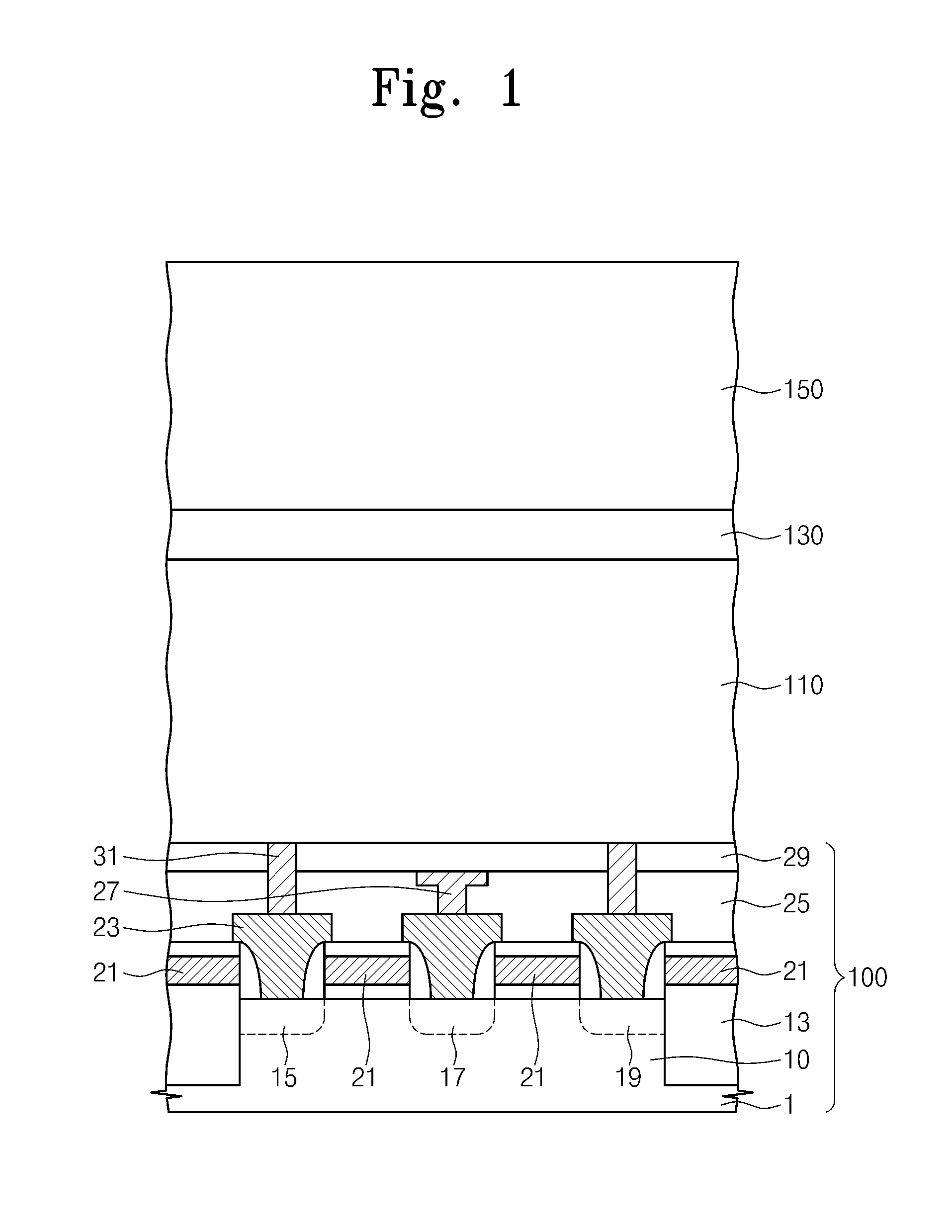
This U.S. non-provisional patent application claims priority under 35 U.S.C. §119 to Korean Patent Application No. 10-2011-0020515, filed on Mar. 8, 2011, the entirety of which is incorporated by reference herein. The present disclosure herein relates to methods of fabricating a semiconductor device and, more particularly, to methods of fabricating a semiconductor device having metallic storage nodes. Semiconductor devices, such as dynamic random access memory (DRAM) devices, may employ cell capacitors as data storage elements. As semiconductor devices become more highly integrated, the size of the cell capacitors has been gradually reduced. As cell capacitors become smaller, capacitance of the cell capacitors may become reduced and the soft error rate (SER) of the capacitors may increase. An increase in the SER may be due to alpha particles. Embodiments of the present disclosure are directed to methods of fabricating a semiconductor device. An exemplary method of fabricating a semiconductor device comprises the steps of forming a metal pattern on a substrate, forming a supporter to support the metal pattern, and etching the metal pattern using an etchant including at least an alkaline solution and an oxidant to form a metal electrode, wherein at least a part of a surface of the metal electrode is uneven. An exemplary method of fabricating a dynamic random access memory (DRAM) cell comprises the steps of forming a substrate including one or more electrodes and an active region, sequentially forming a first mold layer, a support layer and a second mold layer on the substrate, forming a metal pattern penetrating the first mold layer, the support layer and the second mold layer, and wet etching at least a part of a surface of the metal pattern using a wet etchant to form a metal electrode, wherein the part of the surface of the metal electrode that has been formed by etching is uneven. An exemplary method of fabricating a dynamic random access memory (DRAM) cell comprises the steps of forming a substrate including one or more electrodes and an active region, sequentially forming a first mold layer, a support layer and a second mold layer on the substrate, forming a metal pattern penetrating the first mold layer, the support layer and the second mold layer, and etching the metal pattern to form a metal electrode, wherein a first part of a surface of the metal electrode is perpendicular to a surface of the substrate and a second part of the surface of the metal electrode is parallel to a surface of the substrate, and the first and the second parts of a surface of the metal electrode include a jagged surface. The above and other aspects and features of the disclosure will become more apparent by describing in detail exemplary embodiments thereof with reference to the attached drawings, in which: The present disclosure will now be described more fully hereinafter with reference to the accompanying drawings, in which various embodiments are shown. The invention may, however, be embodied in many different forms and should not be construed as limited to the embodiments set forth herein. In the drawings, the size and relative sizes of layers and regions may be exaggerated for clarity. Like numbers refer to like elements throughout. The terminology used herein is for the purpose of describing particular embodiments only and is not intended to be limiting of the invention. As used herein, the singular terms “a,” “an” and “the” should not exclude the plural forms as well, unless the context clearly indicates otherwise. As used herein, the term “and/or” includes any and all combinations of one or more of the associated listed items. It will be understood that when an element or layer is referred to as being “on,” “connected,” or “coupled” to another element or layer, it may be directly on, connected or coupled to the other element or layer or intervening elements or layers may be present. In contrast, when an element or layer is referred to as being “directly on,” “directly connected,” or “directly coupled” to another element or layer, there are no intervening elements or layers present. Similarly, it will be understood that when an element such as a layer, region or substrate is referred to as being “between” two different elements, it can be directly interposed between the two different elements without any intervening element or intervening elements may be present therebetween. In contrast, when an element is referred to as being “directly between” two different elements, there are no intervening elements present. It will be further understood that the terms “comprises”, “comprising,” “includes” and/or “including”, when used herein, specify the presence of stated features, integers, steps, operations, elements, and/or components, but do not preclude the presence or addition of one or more other features, integers, steps, operations, elements, components, and/or groups thereof. Embodiments in the detailed description will be described referring to plan views and/or sectional views by way of ideal schematic views. Accordingly, the exemplary views may be modified depending on manufacturing techniques and/or tolerances. Therefore, the disclosed embodiments are not limited to those shown in the views, but include modifications in configuration formed on the basis of the manufacturing processes. It will be also understood that, although the terms first, second, third etc. may be used herein to describe various elements, these elements should not be limited by these terms. These terms are only used to distinguish one element from another element. Thus, a first element in some embodiments could be termed a second element, and, similarly, a second element could be termed a first element without departing from the teachings of the disclosure. Unless otherwise defined, all terms (including technical and scientific terms) used herein have the same meaning as commonly understood by one of ordinary skill in the art to which this disclosure belongs. It will be further understood that terms, such as those defined in commonly used dictionaries, should be interpreted as having a meaning that is consistent with their meaning in the context of the relevant art/or or the present application, and should not be interpreted in an idealized or overly formal sense unless expressly defined so herein. Metal electrodes may be employed as storage nodes of the semiconductor devices to improve characteristics of the cell capacitors. In order to increase the capacitance of the cell capacitors, it may be beneficial to increase a surface area of the metal electrodes of the cell capacitors. If the height of the metal electrodes is increased, at least one of the metal electrodes may lean to contact the adjacent metal electrode. This leaning effect may cause a malfunction during operation of the semiconductor device. In order to solve the leaning effect, a supporter may be disposed between the metal electrodes. The supporter may be formed of a silicon nitride layer having an etch selectivity that corresponds to a silicon oxide layer used in the formation of mold layers and/or interlayer dielectric layers. The metal patterns may be etched using an acid solution to form metal electrodes that have an uneven surface. The supporter formed of a silicon nitride layer may be etched or removed by the acid solution because the silicon nitride layer exhibits a relatively high etching rate in the acid solution. The supporter may be damaged while the metal patterns are etched using the acid solution. Referring to In one embodiment, a plurality of contact pads 23 are formed on the substrate on which the common drain region 17 and the source regions 15 and 19 have been formed. One of the contact pads 23 may be electrically connected to the common drain region 17; the other two contact pads 23 may be electrically connected to the source regions 15 and 19 respectively. In one embodiment, an insulation layer 25 is formed on the substrate on which the contact pads 23 have been formed, and a bit line 27 is formed in the insulation layer 25. The bit line 27 may be electrically connected to the common drain region 17. An etch stop layer 29 may be formed on the substrate on which the bit line 27 has been formed. A pair of contact plugs 31 may be formed to penetrate the etch stop layer 29 and the insulation layer 25. One of the pair of contact plugs 31 may be electrically connected to the source region 15, and the other contact plug 31 may be electrically connected to the source region 19. In one embodiment, a first mold layer 110 and a second mold layer 150 are sequentially formed on the substrate 100 on which the pair of contact plugs 31 has been formed. The first and second mold layers 110 and 150 may be formed, for example, of a silicon oxide layer. In one embodiment, a support layer 130 is formed between the first and second mold layers 110 and 150. The support layer 130 may be formed, for example, of a material layer having a lower etch rate than the first and second mold layers 110 and 150. For example, the support layer 130 may be formed of a silicon nitride layer. Referring to A conductive layer 190 is formed on the substrate on which the opening 170 is formed. For example, the conductive layer 190 may be conformally formed along the side walls and bottom of the opening so as to not fully fill the opening 170. The conductive layer 190 may be formed, for example, of a metal layer. The conductive layer 190 may be formed to include at least one of a titanium layer, a titanium nitride layer, a ruthenium layer, a tungsten layer, a tungsten nitride layer, a tantalum layer and a tantalum nitride layer. In one embodiment, a sacrificial layer 210 is formed on the substrate on which the conductive layer 190 has been formed. In one embodiment, the sacrificial layer 210 may be formed, for example, of a silicon oxide layer. In one embodiment, the sacrificial layer 210 may be formed of a material layer having a high etch selectivity in comparison to the first and second mold layers 110 and 150. Referring to Referring to In one embodiment, only the surface of the metal electrode 193 that has been subject to etching is uneven. In this embodiment, the remainder of the surface of the metal electrode 193 is even. In one embodiment, each surface or portion of a surface of the metal electrode 193 that has not been subject to etching may be parallel with or perpendicular to a surface of the substrate 1. For example, the bottom surface 193 In one embodiment, the etchant includes at least an alkaline solution and an oxidant. The alkaline solution may include, for example, at least one of ammonium hydroxide (NH4OH), tetra-methyl ammonium hydroxide (TMAH), sodium hydroxide (NaOH), potassium hydroxide (KOH) and choline (C5H15O2N). The oxidant may include, for example, at least one of hydrogen peroxide (H2O2), ozone (O3), sulfuric acid (H2SO4) and nitric acid (HNO3). In one embodiment, the etchant may be formed by mixing hydrogen peroxide (H2O2), ammonium hydroxide (NH4OH) and de-ionized water in a volume ratio of, for example, 4:1:20, respectively. In another embodiment, the etchant further includes at least one of a chelating agent and a fluoride. The chelating agent may include, for example, at least one of an aliphatic amine type compound, a thiol type compound, a crown ether type compound, a hetero aromatic type compound and a carboxylic acidic type compound. The fluoride may include, for example, at least one of hydrofluoric acid (HF) and ammonium fluoride (NH4F). In one embodiment, the etchant is capable of etching the metal patterns 191 to form the uneven surfaces of the metal electrode 193. In this embodiment, the use of the etchant also does not result in damage to the support layer 130 during the formation of the uneven surfaces of the metal electrode 193. Referring to Referring to Now, a method of fabricating a semiconductor device according to another exemplary embodiment will be described with reference to Referring to In the present embodiment, the uneven surface may be formed at inner sidewalls 195 Referring to Referring to A method of fabricating a semiconductor device according to still another exemplary embodiment will be described with reference to Referring to The metal electrode 197 may have a first and second inner sidewall 197 In the present embodiment, the uneven surface may be formed at inner sidewalls 197 In one embodiment, each surface or portion of a surface of the metal electrode 197 that has not been subject to etching may be parallel with or perpendicular to a surface of the substrate 1. For example, the bottom surface 197 Referring to Referring to In one embodiment, the metal pattern 191 is etched to have at least a portion of the surface in at least one of the openings be uneven. The amount of surface area of the resulting metal electrode, for example, metal electrode 193, 195 or 197, that is uneven corresponds to the amount of surface area of the metal pattern 191 that is etched using the etchant. In this embodiment, the surface area of the uneven surface of the resulting metal electrode 193, 195, or 197 is greater than the surface area of the corresponding surface of the metal pattern 191 before etching. Referring to The surface area of the metal electrode 199 that has been etched is greater than the corresponding surface area of the metal pattern 191 exposed and ready to be etched. The area of the metal electrode 199 that has been etched may have an uneven surface. A portion of the metal electrode 199 of a length (e.g. L2) that does not have an etched surface has a lower surface area than a portion of the metal electrode 199 of an equivalent length (e.g. L1 In one embodiment, parts of an uneven surface of the metal electrode 199 may overlap each other in one or more directions (e.g. vertical and/or horizontal directions). The width between the inner sidewall 199 In one embodiment, each surface or portion of a surface of the metal electrode 199 that has not been subject to etching may be parallel with or perpendicular to a surface of the substrate. For example, a surface of the metal electrode 199 which is adjacent to the supporter 131 that has not been subject to etching may be perpendicular to the bottom surface of the substrate 1 and/or with the etch stop layer 29. For example, a portion of the outer sidewall 199 According to the embodiments set forth above, metal patterns are etched using an etchant to form metal electrodes having uneven surfaces. Thus, a surface area of the respective metal electrodes may be increased. As shown in the close-up views of the metal pattern 191 and the metal electrode 199 in The above-disclosed subject matter is to be considered illustrative and not restrictive, and the appended claims are intended to cover all such modifications, enhancements, and other embodiments, which fall within the true spirit and scope of the disclosed embodiments. Thus, the invention is to be determined by the broadest permissible interpretation of the following claims and their equivalents, and shall not be restricted or limited by the foregoing detailed description. The present disclosure describes methods of fabricating a semiconductor device. An exemplary method includes forming a metal pattern on a substrate and etching the metal pattern using an etchant including at least an alkaline solution and an oxidant to form a metal electrode, where at least a portion of the surface of the metal electrode is uneven. 1. A method of fabricating a semiconductor device, the method comprising:
forming a metal pattern on a substrate; forming a supporter to support the metal pattern; and etching the metal pattern using an etchant including at least an alkaline solution and an oxidant to form a metal electrode, wherein at least a part of a surface of the metal electrode is uneven. 2. The method of 3. The method of 4. The method of 5. The method of 6. The method of 7. The method of 8. The method of 9. A method of fabricating a dynamic random access memory (DRAM) cell, the method comprising:
forming a substrate including one or more electrodes and an active region; sequentially forming a first mold layer, a support layer and a second mold layer on the substrate; forming a metal pattern penetrating the first mold layer, the support layer and the second mold layer; and wet etching at least a part of a surface of the metal pattern using a wet etchant to form a metal electrode; wherein the part of the surface of the metal electrode that has been formed by etching is uneven. 10. The method of 11. The method of 12. The method of 13. The method of 14. The method of 15. The method of 16. A method of fabricating a dynamic random access memory (DRAM) cell, the method comprising:
forming a substrate including one or more electrodes and an active region; sequentially forming a first mold layer, a support layer and a second mold layer on the substrate; forming a metal pattern penetrating the first mold layer, the support layer and the second mold layer; and etching the metal pattern to form a metal electrode; wherein a first part of a surface of the metal electrode is perpendicular to a surface of the substrate and a second part of the surface of the metal electrode is parallel with a surface of the substrate, and the first and second parts of a surface of the metal electrode include a jagged surface. 17. The method of 18. The method of 19. The method of the jagged surface of the metal electrode comprises at least one of a first portion and a second portion, the first portion of the jagged surface from a first point to a second point in a first direction has an equal length to the second portion of the jagged surface from a third point to a fourth point in the first direction, and the surface area of the first portion is different than the surface area of the second portion. 20. The method of the jagged surface of the metal electrode has an equal length to a surface of the metal electrode has not been subject to the etching, and the surface area of the jagged surface of the metal electrode is greater than the surface of the metal electrode has not been subject to the etching CROSS-REFERENCE TO RELATED APPLICATIONS
BACKGROUND
SUMMARY
BRIEF DESCRIPTION OF THE DRAWINGS
DETAILED DESCRIPTION OF THE EMBODIMENTS