METHOD OF MANUFACTURING MULTILAYER WIRING SUBSTRATE
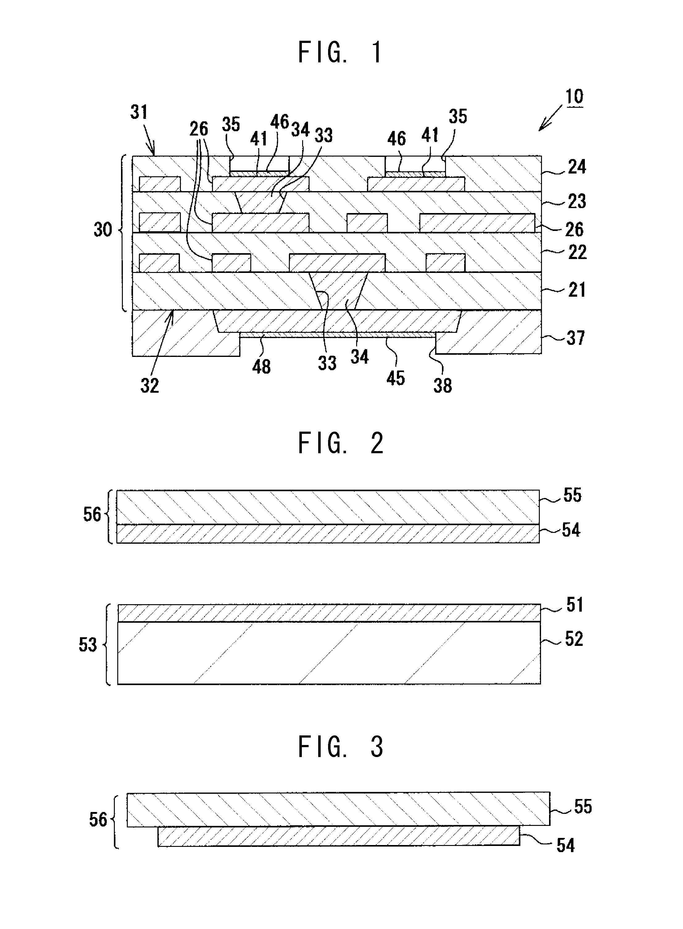
The present application claims priority from Japanese Patent Application No. 2010-240610, which was filed on Oct. 27, 2010, the disclosure of which is herein incorporated by reference in its entirety. 1. Field of the Invention The present invention relates to a method of manufacturing a multilayer wiring substrate having a multilayer structure in which a plurality of resin insulation layers and a plurality of conductor layers are laminated alternately. 2. Description of Related Art In association with recent increasing tendency toward higher operation speed and higher functionality of semiconductor integrated circuit devices (IC chips) used as, for example, microprocessors of computers, the number of terminals increases, and the pitch between the terminals tends to become narrower. Generally, a large number of terminals are densely arrayed on the bottom surface of an IC chip and flip-chip-bonded to terminals provided on a motherboard. However, since the terminals of the IC chip differ greatly in pitch from those of the motherboard, difficulty is encountered in bonding the IC chip directly onto the motherboard. Thus, according to an ordinarily employed method, a semiconductor package configured such that the IC chip is mounted on an IC chip mounting wiring substrate is fabricated, and the semiconductor package is mounted on the motherboard. The IC chip mounting wiring substrate which partially constitutes such a semiconductor package has been has been put to practical use in the form of a multilayer substrate configured such that a build-up layer is formed on the front and back surfaces of a substrate core. The substrate core used in the multilayer wiring substrate is, for example, a resin substrate (glass epoxy substrate or the like) formed by impregnating reinforcement fiber with resin. Through utilization of rigidity of the substrate core, resin insulation layers and conductor layers are laminated alternately on the front and back surfaces of the substrate core, thereby forming respective build-up layers. In the multilayer wiring substrate, the substrate core serves as a reinforcement and is formed very thick as compared with the build-up layers. Also, the substrate core has conductor lines (specifically, through-hole conductors, etc.) extending therethrough for electrical communication between the build-up layers formed on the front and back surfaces. In recent years, in association with implementation of high operation speeds of semiconductor integrated circuit devices, signal frequencies to be used have become those of a high frequency band. In this case, the conductor lines which extend through the substrate core serve as sources of high inductance, leading to the transmission loss of high-frequency signals and the occurrence of circuitry malfunction and thus hindering implementation of high operation speed. In order to solve this problem, a multilayer wiring substrate having no substrate core is proposed (refer to, for example, Patent Documents 1 and 2). The multilayer wiring substrates described in Patent Documents 1 and 2 do not use a substrate core, which is relatively thick, thereby reducing the overall wiring length. Thus, the transmission loss of high-frequency signals is lowered, whereby a semiconductor integrated circuit device can be operated at high speed. The multilayer wiring substrate shown in Patent Document 1 is manufactured by the following method. As shown in The multilayer wiring substrate shown in Patent Document 2 is manufactured by the method shown in The above-described multilayer wiring substrate manufacturing method disclosed in Patent Document 1 uses the separable copper foil 83, which is a special member. Since this separable copper foil 83 is expensive as compared with ordinary copper foil, the multilayer wiring substrate requires a higher manufacturing cost. Furthermore, in the case of the method disclosed in Patent Document 2, the ground layer 92 and the support metal layer 93 formed of two copper foils must be bonded onto the support substrate body 91 through application of heat and pressure onto the support substrate 94, which is a resin substrate. As described above, since a heat and pressure application step is additionally required for preparation of the support substrate 94, manufacturing cost increases. Moreover, in the case of the method disclosed in Patent Document 2, as shown in The present invention has been conceived in view of the above problems, and an object of the invention is to provide a method of manufacturing a multilayer wiring substrate which can reduce manufacturing cost. A means (Means 1) for solving the above problems is a method of manufacturing a multilayer wiring substrate having a multilayer structure in which a plurality of resin insulation layers and a plurality of conductor layers are laminated alternately. The method comprising an insulation layer fixation step of laying a lower metal foil and an upper metal foil directly on each other, disposing the lower metal foil and the upper metal foil on a support base material such that the upper metal foil and a peripheral edge portion of the lower metal foil are exposed (i.e., exposed at the surface side of the support base material), adhering a resin insulation material (which is to become one resin insulation layer) to a surface of the upper metal foil, and fixing a peripheral edge portion of the resin insulation material to the support base material; a lamination step of laminating the conductor layers and the resin insulation layers so as to obtain a laminate structure having, on the upper metal foil, a wiring laminate portion which is to become the multilayer wiring substrate; a removal step of cutting, after the lamination step, the laminate structure along a boundary between the wiring laminate portion and a surrounding portion located around the wiring laminate portion, to thereby remove the surrounding portion; and a separation step of separating the wiring laminate portion from the support base material along a boundary between the upper and lower metal foils. According to the invention described in Means 1, a coreless multilayer wiring substrate can be manufactured through use of upper and lower metal foils, which are ordinary metal foils, without use of a separable copper foil, which is a special metal foil used in the method disclosed in Patent Document 1. Therefore, material cost can be reduced. Furthermore, the lower metal foil of the present invention is larger in outer shape than the upper metal foil, and, in the insulation layer fixation step, the metal foils are disposed on the support base material such that the upper metal foil and a peripheral edge portion of the lower metal foil are exposed at the surface. The resin insulation material, which is to become one of the resin insulation layers, is then adhered to the surface of the upper metal foil, and a peripheral edge portion of the resin insulation material is fixed to the support base material. This procedure enables the copper foil to be fixed to the support base material by making use of the step of forming the resin insulation layer. Therefore, the method of the present embodiment does not require a dedicated step for fixing a support metal layer to a support substrate as in the case of the method disclosed in Patent Document 2. As a result, the manufacturing cost of the multilayer wiring substrate can be reduced. Additionally, in the insulation layer fixation step, the upper copper foil is pressed by the resin insulation material, which has flowability, and a peripheral edge portion of the resin insulation material is fixed to the support base material. Therefore, a step is hardly formed on the surface of the upper copper foil, and positioning in the lamination step can be performed accurately. In accord with another aspect of the invention, a method of manufacturing a multilayer wiring substrate comprises a preparation step of preparing a metal-foil-clad support base material which includes a support base material and a lower metal foil provided on a surface of the support base material, and a metal-foil-clad resin insulation material which includes a resin insulation material and an upper metal foil provided on the surface of the resin insulation material; a metal foil removal step of removing a peripheral edge portion of the upper metal foil of the metal-foil-clad resin insulation material. Rather than a special material, general purpose materials which are generally used in manufacture of the multilayer wiring substrate can be used as the metal-foil-clad support base material and the metal-foil-clad resin insulation material. Notably, the resin insulation material prepared in this preparation step is an insulation material which is to become the outermost resin insulation layer exposed on the side toward one main face of the multilayer wiring substrate. According to this aspect, in the insulation layer fixation step, the upper metal foil of the metal-foil-clad resin insulation material is brought into contact with the lower metal foil of the metal-foil-clad support base material, and a peripheral edge portion of the resin insulation material exposed as a result of removal of a peripheral edge portion of the upper metal foil is adhered to the lower metal foil of the metal-foil-clad support base material, whereby the metal-foil-clad resin insulation material is fixed to the metal-foil-clad support base material. In this case, portions of the upper metal foil and the lower metal foil which contact with each other do not adhere to each other, and a peripheral edge portion of the resin insulation material is adhered to the lower metal foil of the support base material. In the lamination step, the plurality of conductor layers and the plurality of resin insulation layers are laminated in order to form a laminate structure. In the removal step, the laminate structure is cut along the boundary between the wiring laminate portion, which is to become a multilayer wiring substrate, and a surrounding portion around the wiring laminate portion, whereby a peripheral edge portion of the laminate structure where the resin insulation material and the lower metal foil of the support base material adhere together is removed. As a result, the wiring laminate portion becomes separable from the support base material at a position where the upper metal foil and the lower metal foil contact with each other (the boundary between the two metal foils). In the separation step, the wiring laminate portion is separated from the support base material along the boundary between the two metal foils. In the preparation step, preferably, the support base material is formed by use of a material whose coefficient of thermal expansion is approximately equal to those of the resin insulation layers. In this case, in the lamination step, thermal stress becomes unlikely to concentrate at the interface between the support base material and the resin insulation layers laminated thereon. Therefore, problems such as formation of wrinkles on the copper foils can be avoided. Notably, the phrase “the support base material is formed of a material whose coefficient of thermal expansion is approximately equal to those of the resin insulation layers” means that the difference between the coefficient of thermal expansion of the support base material and that of the resin insulation layers falls within a range of ±5 ppm/° C. Another means (Means 2) for solving the above problems is a method of manufacturing a multilayer wiring substrate having a laminate structure in which a plurality of resin insulation layers and a plurality of conductor layers are laminated alternately. The method comprises an insulation layer fixation step of disposing a single metal foil on a support base material, adhering a resin insulation material, which is to become one resin insulation layer, to a surface of the single metal foil, and fixing a peripheral edge portion of the resin insulation material to a surface of the support base material; a lamination step of laminating the conductor layers and the resin insulation layers so as to obtain a laminate structure having, on the single metal foil, a wiring laminate portion, which is to become the multilayer wiring substrate; a removal step of cutting, after the lamination step, the laminate structure along a boundary between the wiring laminate portion and a surrounding portion located around the wiring laminate portion, to thereby remove the surrounding portion; and a separation step of separating the wiring laminate portion from the support base material along the single metal foil (i.e., along a surface of the single metal foil). According to the invention described in Means 2, a coreless multilayer wiring substrate can be manufactured through use of a single metal foil without use of a separable copper foil, which is a special metal foil used in the conventional technique. In this case, material cost can be reduced, whereby manufacturing cost of the multilayer wiring substrate can be reduced. Preferably, the metal foil(s) is a copper foil(s); and the method further comprises a terminal formation step of forming external terminals through patterning of the copper foil exposed at the surface of the wiring laminate portion after the separation step. In this case, since the copper foil used for separating the wiring laminate portion and the support base material from each other becomes the external terminals of the multilayer wiring substrate, manufacturing cost can be reduced as compared with the case where the external terminals are formed by use of another copper foil or copper plating. Furthermore, in the case where, like the invention described in Means 1, lower and upper copper foils are laid directly on each other and are disposed on the support base material in the insulation layer fixation step, the lower copper foil is made larger in outer shape than the upper copper foil so that the upper copper foil does not project from the peripheral edge portion of the lower copper foil. In this case, even when the resin insulation material is caused to adhere to the surface of the upper copper foil and press the upper copper foil, the flatness of the upper copper foil can be secured sufficiently. Accordingly, in the terminal formation step, external terminals having a high degree of flatness can be formed through patterning of the upper copper foil exposed at the surface of the wiring laminate portion. Examples of the external terminals formed in the terminal formation step include connection terminals to which an IC chip or a chip capacitor is connected, and connection terminals to which a motherboard is connected. The method of manufacturing a multilayer wiring substrate may further comprise a roughening step of roughening the surface of the metal foil to which the resin insulation material is adhered. In this case, since the resin insulation material, which is to later become one of the resin insulation layers, adheres to the metal foil without fail, the plurality of conductor layers and the plurality of resin insulation layers can be laminated without fail in the lamination step. The plurality of resin insulation layers which partially constitute the multilayer wiring substrate can be selected freely in consideration of electrical insulating performance, heat resistance, humidity resistance, etc. Preferred examples of a polymeric material used to form the resin insulation layers include thermosetting resins, such as epoxy resin, phenol resin, urethane resin, silicone resin, and polyimide resin; and thermoplastic resins, such as polycarbonate resin, acrylic resin, polyacetal resin, and polypropylene resin. Examples of the filler contained in the resin insulation layers include filters formed of inorganic oxides, such as silica, titania, and alumina. In particular, since silica filler is low in dielectric constant and coefficient of linear thermal expansion, addition of silica filler to the resin insulation layers further enhance the quality of the multilayer wiring substrate. The support base material may be a resin plate formed of a completely cured resin material or a metal plate formed of a metallic material. The resin material and metal material for forming the support base material may be those which are inexpensive and relatively hard. However, in the case where the laminate structure is cut together with the support base material in the removal step, preferably, a resin substrate which can be readily cut is used as the support base material. Illustrative aspects of the invention will be described in detail with reference to the following figures wherein: A method of manufacturing multilayer wiring substrate according to a first embodiment of the present invention will next be described in detail with reference to the drawings. As shown in In the present embodiment, the plurality of connection terminals 41 are IC-chip connection terminals to which an IC chip is connected, and are disposed in an array on the top surface 31 side of the wiring laminate portion 30. Meanwhile, on the opposite side of the wiring laminate portion 30 where a bottom surface 32 thereof is present, a plurality of connection terminals 45 for LGA (land grid array) to which a motherboard is connected are disposed in an array. The motherboard connection terminals 45 are greater in area than the IC-chip connection terminals 41 on the top surface 31 side. Via holes 33 and filled-via conductors 34 are provided in the resin insulation layers 21, 22, and 23. The via conductors 34 are shaped such that their diameters increase in the same direction (in A plurality of openings 35 are formed in the fourth resin insulation layer 24 exposed to the outside on the top surface 31 side of the wiring laminate portion 30. The IC chip connection terminals 41 are disposed in the openings 35 such that their upper surfaces become lower than the surface of the resin insulation layer 24. Peripheral portions of the upper surfaces of the IC chip connection terminals 41 are buried in the resin insulation layer 24. The IC-chip connection terminals 41 are made mainly of a copper layer. Furthermore, the IC-chip connection terminals 41 have a structure in which a plating layer 46 of a material other than copper (specifically, a nickel-gold plating layer) covers only the upper surface of the copper layer serving as a main constituent of the IC-chip connection terminals 41. On the bottom surface 32 side of the wiring laminate portion 30, the surface of the resin insulation layer 21 is covered substantially completely by a solder resist layer 37. The solder resist layer 37 has openings 38 therein so as to expose the motherboard connection terminals 45. In the present embodiment, the openings 38 are smaller in size than the motherboard connection terminals 45, and peripheral portions of the lower surfaces of the motherboard connection terminals 45 are buried in the solder resist layer 37. The motherboard connection terminals 45 are made mainly of a copper layer. Furthermore, the motherboard connection terminals 45 have a structure in which a plating layer 48 of a material other than copper (specifically, a nickel-gold plating layer) covers only the lower surface of the copper layer serving as a main constituent of the motherboard connection terminals 45. The thus-configured multilayer wiring substrate 10 is fabricated by, for example, the following procedure. First, in a preparation step, as shown in In the present invention, the “coefficient of thermal expansion” refers to the coefficient of thermal expansion as measured in a direction (x-y direction) perpendicular to the thickness direction (z direction). The coefficient of thermal expansion is measured for a range of 0° C. to 100° C. through TMA (thermomechanical analysis), which is defined in, for example, JPCA-BU01. Then, in a metal foil removal step, a peripheral edge portion of the copper foil 54 of the copper-foil-clad build-up material 56 is removed (see Subsequently, in an insulation layer fixation step, the copper foil 54 of the copper-foil-clad build-up material 56 is brought into contact with the copper foil 51 of the support substrate 53, and the resin insulation material 55 exposed at the peripheral edge portion of the copper-foil-clad build-up material 56 is adhered to the copper foil 51 of the support substrate 53. Thus, the resin insulation material 55, which will become the resin insulation layer 21, is fixed to the support substrate 53 (see Subsequently, as shown in After the desmear step, electroless copper plating and copper electroplating are performed by a known process, thereby forming the via conductors 34 in the via holes 33. Further, etching is performed by a known process (e.g., semi-additive process), thereby forming the conductor layer 26 in a predetermined pattern on the resin insulation layer 21 (see Also, the second to fourth resin insulation layers 22 to 24 and the corresponding conductor layers 26 are formed and laminated on the resin insulation layer 21 by processes similar to those used to form the first resin insulation layer 21 and the associated conductor layer 26 (lamination step). By the above-described steps, there is formed a wiring laminate 60 in which the copper foils 51 and 54, the resin insulation layers 21 to 24, and the conductor layers 26 are laminated on the support substrate 52 (see Subsequently, as shown in After the desmear step, the wiring laminate 60 is cut by a dicing apparatus (not shown) so as to remove a surrounding portion around the wiring laminate portion 30 (removal step). At this time, as shown in Subsequently, as shown in Next, photosensitive epoxy resin is applied onto the resin insulation layer 21 and is cured so as to form the solder resist layer 37. Exposure and development are then performed with a predetermined mask placed thereon so as to form the openings 38 in the solder resist layer 37. After that, electroless nickel plating and electroless gold plating are successively performed on the surfaces (upper surfaces) of the IC-chip connection terminals 41 exposed from the openings 35 and on the surfaces (lower surfaces) of the motherboard connection terminals 45 exposed from the openings 38, whereby the nickel-gold plating layers 46 and 48 are formed. Through the above-described steps, the multilayer wiring substrate 10 of Therefore, the present embodiment can yield the following effects. (1) In the present embodiment, the coreless multilayer wiring substrate 10 can be manufactured through use of the copper-foil-clad support substrate 53 and the copper-foil-clad build-up material 56, without use of the separable copper foil 83, which is a special metal foil used in the method disclosed in Patent Document 1. In place of a special material, general purpose materials which are generally used in manufacture of the multilayer wiring substrate can be used as the copper-foil-clad support substrate 53 and the copper-foil-clad build-up material 56. Therefore, material cost can be reduced, as compared with the conventional technique. (2) In the present embodiment, in the insulation layer fixation step, the copper foil 54 of the copper-foil-clad build-up material 56 is brought into contact with the copper foil 51 of the support substrate 53, and a peripheral edge portion of the resin insulation material 55 exposed through removal of a peripheral edge portion of the copper foil 54 is adhered to the copper foil 51 of the support substrate 53, whereby the resin insulation layer 21 is fixed to the support substrate 53. This procedure enables the copper foil 54 to be fixed to the support substrate 53 by making use of the step of forming the resin insulation layer 21. Therefore, the method of the present embodiment does not require a dedicated step (see (3) In the present embodiment, the support substrate 52 is formed by use of a material whose coefficient of thermal expansion is the same as that of the resin insulation layers 21 to 24. In this case, in the lamination step, thermal stress becomes unlikely to concentrate at the interface between the support substrate 52 and the resin insulation layers 21 to 24 laminated thereon. Therefore, problems such as formation of wrinkles on the copper foils 51 and 54 can be avoided. (4) In the present embodiment, in the terminal formation step, the motherboard connection terminals 45 are formed through patterning of the copper foil 54 utilized for separation of the wiring laminate portion 30 from the support substrate 53. Thus, the manufacturing cost of the multilayer wiring substrate 10 can be reduced, as compared with the case where the motherboard connection terminals 45 are formed from another copper foil or copper plating. (5) In the present embodiment, the lower copper foil 51 is larger in outer shape than the upper copper foil 54, and, in the insulation layer fixation step, the upper copper foil 54 is disposed on the support substrate 53 such that the upper copper foil 54 does not project from the peripheral edge of the lower copper foil 51. In this case, even when the resin insulation material 55 of the build-up material 56 is pressed from the upper side, the flatness of the upper copper foil 54 can be secured sufficiently. Accordingly, in the terminal formation step, the motherboard connection terminals 45 having a high degree of flatness can be formed through patterning of the copper foil 54 exposed at the surface of the wiring laminate portion 30. Thus, the connection reliability of the motherboard connection terminals 45 can be secured sufficiently. Notably, the embodiment of the present invention may be modified as follows. In the above-described embodiment, the multilayer wiring substrate 10 is manufactured by use of the copper-foil-clad support substrate 53 and the copper-foil-clad build-up material 56. However, the method of manufacturing the multilayer wiring substrate 10 is not limited thereto. Specifically, in a preparation step, as shown in Subsequently, in an insulation layer fixation step, as shown in In the above-described insulation layer fixation step, a ground resin insulation layer serving as an adhesive layer may be interposed between the lower copper foil 71 and the support substrate 70. Since this configuration enables bonding of the entire lower surface of the copper foil 71 to the support substrate 70, in the separation step, the separation at the interface between the copper foils 71 and 72 can be performed without fail. Also, the above-described manufacturing steps may further include a surface roughening step of roughening the surface of the copper foil 72, to which the resin insulation material 73 is adhered. When this configuration is employed, the resin insulation material 73, which will later become the resin insulation layer 21, adheres to the copper foil 72 without fail. Therefore, in the lamination step, the plurality of the conductor layers 26 and the plurality of resin insulation layers 21 to 24 can be laminated without fail. In the above-described embodiment, the two copper foils 51 and 54 (71 and 72) are disposed on the support substrate 52 (70) for manufacture of the multilayer wiring substrate 10. The method of manufacturing the multilayer wiring substrate 10 is not limited thereto, and the multilayer wiring substrate 10 may be manufactured by use of a single copper foil. This manufacturing method will be described in detail. In a preparation step, as shown in In the above-described embodiment, the multilayer wiring substrate 10 is manufactured by laminating the resin insulation layers 21 to 24 and the conductor layers 26 from the bottom surface 32 side where the motherboard connection terminals 45 are formed. However, the method of manufacturing the multilayer wiring substrate 10 is not limited thereto. A multilayer wiring substrate may be manufactured by laminating the resin insulation layers 21 to 24 and the conductor layers 26 from the top surface 31 side where the IC chip connection terminals 41 are formed. In this case, in the terminal formation step, the IC chip connection terminals 41 are formed through patterning of the copper foil 54. Furthermore, the plurality of conductors 26 formed in the plurality of resin insulation layer 21 to 24 are connected with one another via conductors 34 whose diameters increase from the top surface 31 side toward the bottom surface 32 side. In the above-described embodiment, the motherboard connection terminals 45 are formed through patterning of the copper foil 54. However, the method of forming the motherboard connection terminals 45 is not limited thereto. For example, in the lamination step, external terminals are formed, through patterning, in advance as a portion of the conductor layer 26 provided between the first resin insulation layer 21 and the second resin insulation layer 22. Subsequently, after the separation step, the copper foil 54 exposed at the bottom surface of the wiring laminate portion 30 is completely removed through etching. After that, laser drilling is performed on the resin insulation layer 21 so as to form openings for exposing the external terminals. Even when this alternative method is employed, a coreless multilayer wiring substrate can be manufactured. Next, technical ideas that the embodiments described above implement are enumerated below. (1) A method of manufacturing a multilayer wiring substrate having a laminate structure in which a plurality of resin insulation layers and a plurality of conductor layers are laminated alternately, the method comprising an insulation layer fixation step of laying a lower metal foil and an upper metal foil directly on each other in an unbonded state, disposing them on a support base material such that the upper metal foil and a peripheral edge portion of the lower metal foil are exposed at the surface of the support base material, adhering an uncured resin insulation material, which is to later become one of the resin insulation layers, to the surface of the upper metal foil, and fixing a peripheral edge portion of the resin insulation material to the support base material; a lamination step of laminating the conductor layers and the resin insulation layers so as to obtain a laminate structure having, on the metal foil, a wiring laminate portion, which is to become the multilayer wiring substrate; a removal step of cutting, after the lamination step, the laminate structure together with the support base material, along a boundary between the wiring laminate portion and a surrounding portion located around the wiring laminate portion, to thereby remove the surrounding portion; and a separation step of separating the wiring laminate portion from the support base material along the boundary between the upper and lower metal foils. (2) The method of manufacturing a multilayer wiring substrate according to the technical idea (1) is characterized by further comprising a surface roughening step of roughening the surface of the metal foil to which the resin insulation material is adhered. (3) The method of manufacturing a multilayer wiring substrate according to the technical idea (1) or (2) is characterized in that the resin insulation material prepared in the preparation step is an insulation material which is to become the outermost resin insulation layer exposed on the side toward one main face of the multilayer wiring substrate. (4) The method of manufacturing a multilayer wiring substrate according to any one of the technical ideas (1) to (3) is characterized in that the support base material is a resin plate formed of a completely cured resin material or a metal plate formed of a metal material. A method of manufacturing a multilayer wiring substrate is provided. A foil of a metal-foil-clad resin insulation material is brought into contact with a foil of a metal-foil-clad support substrate. A peripheral edge portion of the resin insulation material exposed as a result of removal of a peripheral edge portion of the foil is adhered to the foil of the support substrate. A plurality of conductor layers and a plurality of resin insulation layers are laminated so as to obtain a laminate structure having a wiring laminate portion, which is to become the multilayer wiring substrate. The laminate structure is cut along a boundary between the wiring laminate portion and a surrounding portion, and the surrounding portion is removed. The wiring laminate portion is separated from the support substrate along the boundary between the two foils. 1. A method of manufacturing a multilayer wiring substrate having a multilayer structure in which a plurality of resin insulation layers and a plurality of conductor layers are laminated alternately, the method comprising:
an insulation layer fixation step of laying a lower metal foil and an upper metal foil directly on each other, disposing the lower metal foil and the upper metal foil on a support base material such that the upper metal foil and a peripheral edge portion of the lower metal foil are exposed, adhering a resin insulation material to a surface of the upper metal foil, and fixing a peripheral edge portion of the resin insulation material to the support base material; a lamination step of laminating the conductor layers and the resin insulation layers so as to obtain a laminate structure having, on the upper metal foil, a wiring laminate portion which is to become the multilayer wiring substrate; a removal step of cutting, after the lamination step, the laminate structure along a boundary between the wiring laminate portion and a surrounding portion located around the wiring laminate portion, to thereby remove the surrounding portion; and a separation step of separating the wiring laminate portion from the support base material along a boundary between the upper and lower metal foils. 2. A method of manufacturing a multilayer wiring substrate having a multilayer structure in which a plurality of resin insulation layers and a plurality of conductor layers are laminated alternately, the method comprising:
a preparation step of preparing a metal-foil-clad support base material which includes a support base material and a lower metal foil provided on a surface of the support base material, and a metal-foil-clad resin insulation material which includes a resin insulation material and an upper metal foil provided on a surface of the resin insulation material; a metal foil removal step of removing a peripheral edge portion of the upper metal foil of the metal-foil-clad resin insulation material; an insulation layer fixation step of bringing the upper metal foil of the metal-foil-clad resin insulation material into contact with the lower metal foil of the metal-foil-clad support base material, and adhering a peripheral edge portion of the resin insulation material exposed as a result of removal of a peripheral edge portion of the upper metal foil to the lower metal foil of the metal-foil-clad support base material, whereby the metal-foil-clad resin insulation material is fixed to the metal-foil-clad support base material; a lamination step of laminating the conductor layers and the resin insulation layers so as to obtain a laminate structure having, on the upper metal foil, a wiring laminate portion which is to become the multilayer wiring substrate; a removal step of cutting, after the lamination step, the laminate structure along a boundary between the wiring laminate portion and a surrounding portion located around the wiring laminate portion, to thereby remove the surrounding portion; and a separation step of separating the wiring laminate portion from the support base material along a boundary between the upper and lower metal foils. 3. The method of manufacturing a multilayer wiring substrate according to 4. A method of manufacturing a multilayer wiring substrate having a laminate structure in which a plurality of resin insulation layers and a plurality of conductor layers are laminated alternately, the method comprising:
an insulation layer fixation step of disposing a single metal foil on a support base material, adhering a resin insulation material, which is to become one resin insulation layer, to a surface of the single metal foil, and fixing a peripheral edge portion of the resin insulation material to a surface of the support base material; a lamination step of laminating the conductor layers and the resin insulation layers so as to obtain a laminate structure having, on the single metal foil, a wiring laminate portion, which is to become the multilayer wiring substrate; a removal step of cutting, after the lamination step, the laminate structure along a boundary between the wiring laminate portion and a surrounding portion located around the wiring laminate portion, to thereby remove the surrounding portion; and a separation step of separating the wiring laminate portion from the support base material along the single metal foil. 5. The method of manufacturing a multilayer wiring substrate according to 6. The method of manufacturing a multilayer wiring substrate according to 7. The method of manufacturing a multilayer wiring substrate according to CROSS REFERENCE TO RELATED APPLICATIONS
BACKGROUND OF THE INVENTION
RELATED ART DOCUMENTS
Patent Documents
BRIEF SUMMARY OF THE INVENTION
BRIEF DESCRIPTION OF THE DRAWINGS
DETAILED DESCRIPTION OF EXEMPLARY EMBODIMENTS OF THE INVENTION
DESCRIPTION OF REFERENCE NUMERALS