Arrangement with substrate and at least one chip.
The available invention concerns an arrangement with a substrate and at least one chip, that in a masking compound embedded ist.
To the protection against mechanical and partial climatic influences on a print substrate (COB) or than Teli of a Dickfilmoder Dünnfilmechaltung on a ceramic substrate, with thin film is often covered if necessary also on a glass substrate arranged chip in the so-called GlobTop procedure with a drop Expoxy or silicone mass. A system with at least three materials with different develops expands ungskoefíizienten.
The different coefficients of expansion lead to tensions and shearing stresses on chip and bond wires and if necessary to relative shifts (Abecherungen), not only during the production process, which causes a cooling of the masking compound and a Auflöten of additional components, but also later with changing Umgebungsund operation temperatures of the finished Moduls.
Such problems increase with increasing surface of the chips. It becomes particularly problematic, where several, large chips on a substrate are taken off within one Multichip lnsel by the same Glob Top müssen.
In the case of Dickoder thin section ceramic substrates already by the cooling of a Epoxy Glob Tops a substantial deflection of the substrate is determined, those to interruptions in the conductive strips and/or to hair-cracks in the substrate and/or the cover leads kann.
It is from there task of the available Eñindung, an arrangement with a substrate and at least one chip with decreased induced mechanical forces too schaffen.
This task becomes eñindungsgemäss by an arrangement according to requirement 1 gelöst.
Favourable arrangements of the Eñindung are in the further requirements angegeben.
The invention is more near described in the following on the basis a design. Show:
Fig. 1 a schematieche representation of a substrate with a chip and a cover manufactured in the GlobTop procedure, Fig. 2 a similar representation in a substrate bent by induced mechanical forces, Fig. 3 to 9 different with an additional cover provided after sand yielding arrangements the Erfindung.
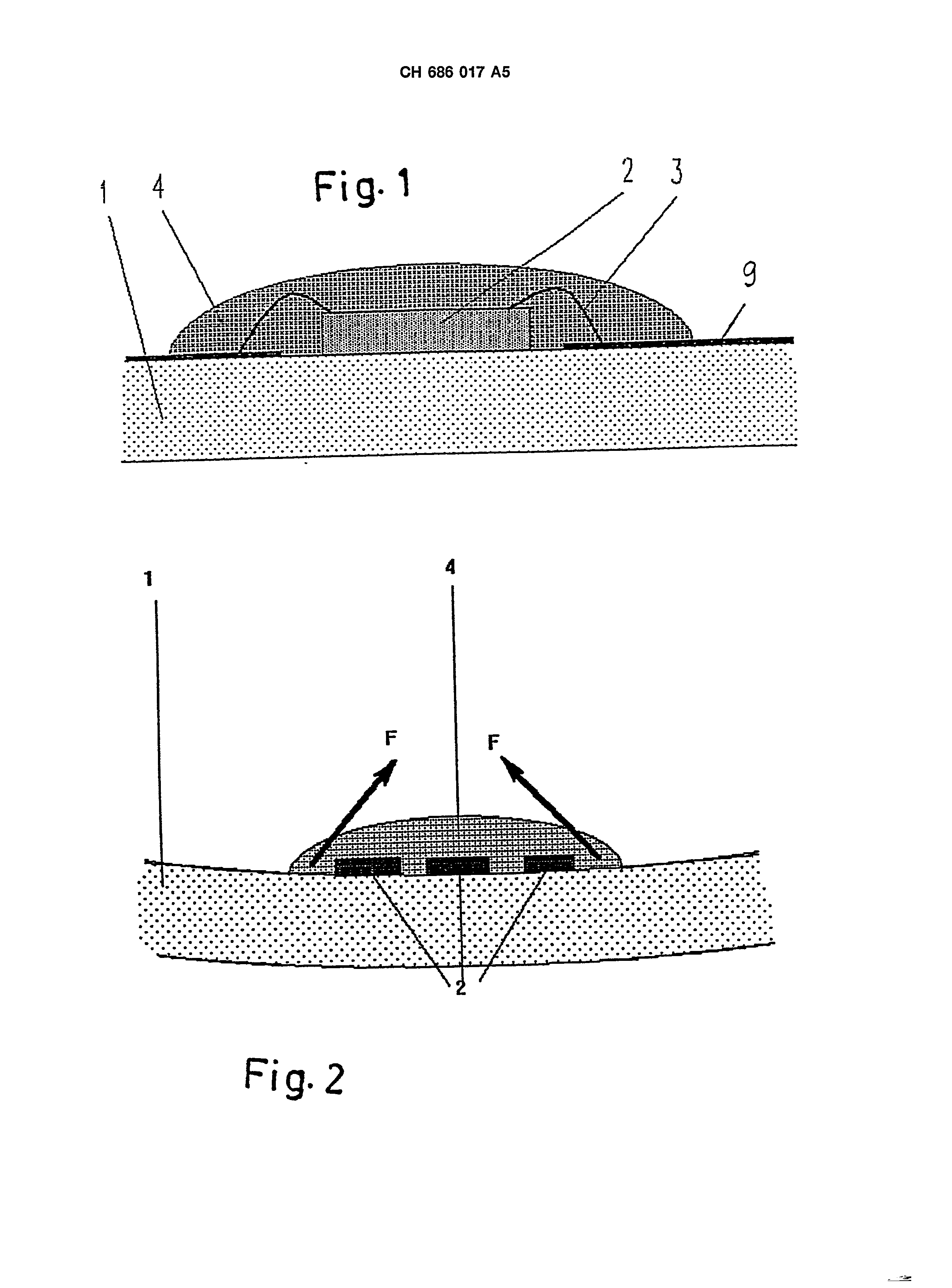
In Fig. 1 represented ideal arrangement after the state of the art exhibits a substrate 1, for example a ceramic(s), a Printoder glass substrate, on a silicon chip 2 connected by bond wires 3 with the substrate metallization g soldered or adhesive ist.
The chip 2 and the bond wires 3 are taken off in the Glob Top procedure by a Epoxyoder silicone mass 4. In the ideal arrangement after Fig. 1 the induced mechanisohen forces become vernachlässigt.
Fig. a similar arrangement shows 2 after the state of the art as Fig. 1 without the forces F, which develop because of the different coefficients of expansion between the substrate 1 and the masking compound 4, arising with the cooling, too vernachlässigen.
The forces F lead to, to the illustration of the effect which can be described practice-rubbed drawn deflection of the substrate and if necessary to tears in the substrate and thus into the conductive strips and/or resistance applied on the upper or lower substrate side and/or in the cover and thus to bonding wire u nterbrüchen.
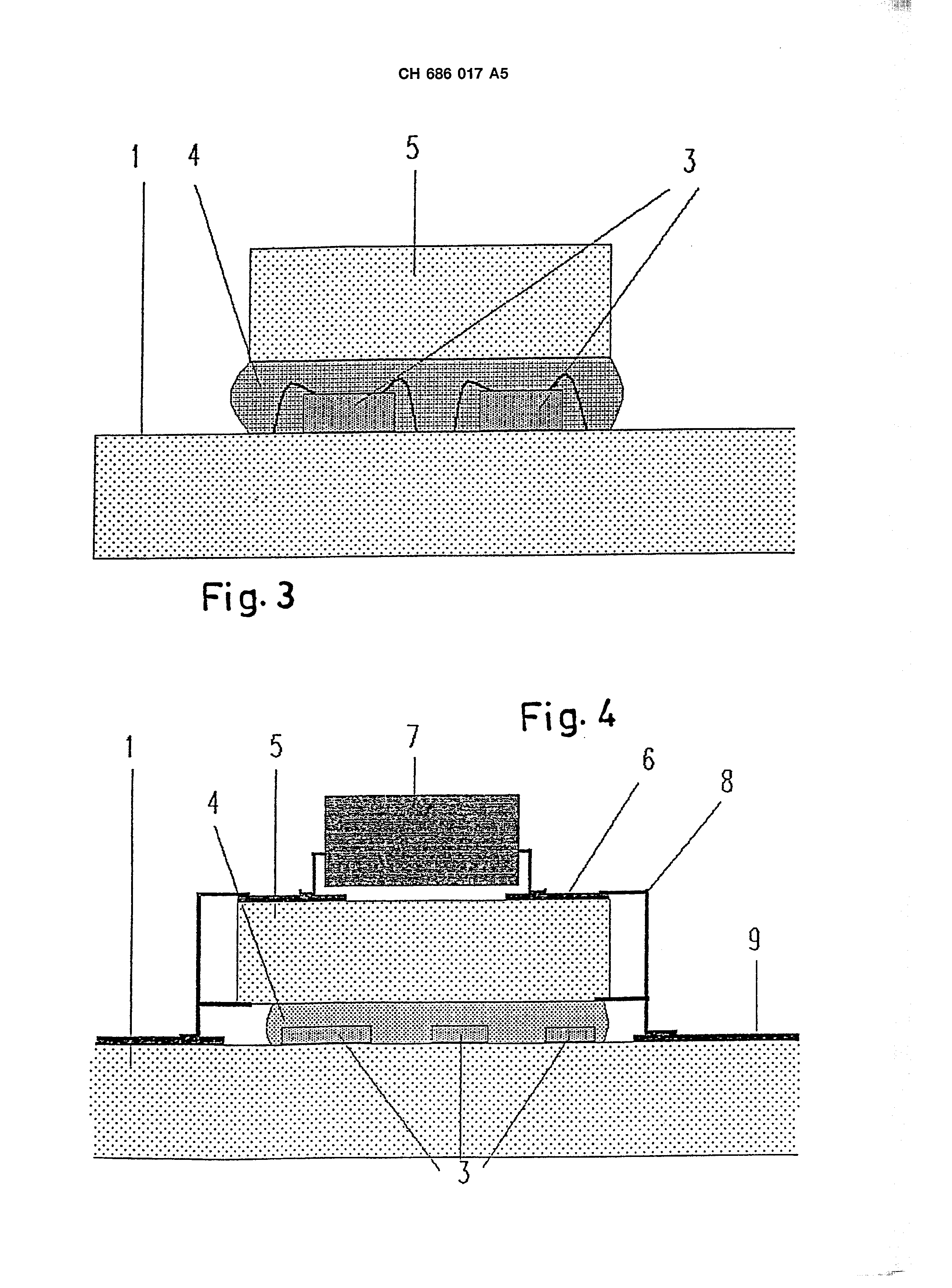
In Fig. 3 represented arrangement after the available invention exhibits a substrate 1, on that several chips 3 under a masking compound 4 applied sind.
In this arrangement additionally a cover from the same or concerning thermal expansion similar material and intended with a similar thickness is as the substrate 1. By a such sand yielding arrangement the problems described above can completely prevented or at least in substantial mass reduced werden.
By the cover 5 above all the bending forces are eliminated, so that the substrate flat bleibt.
Attempts with ceramic substrates and after ceramic(s) covers the Eñindung showed clearly the fact that such an arrangement prevents the deflection of the substrate practically perfectly, even if the cover is selected more thinly than the substrate, which in the interest of as small total an overall height as possible can be desired. In all other respects these attempts have likewise a good temperature change firmness gezeigt.
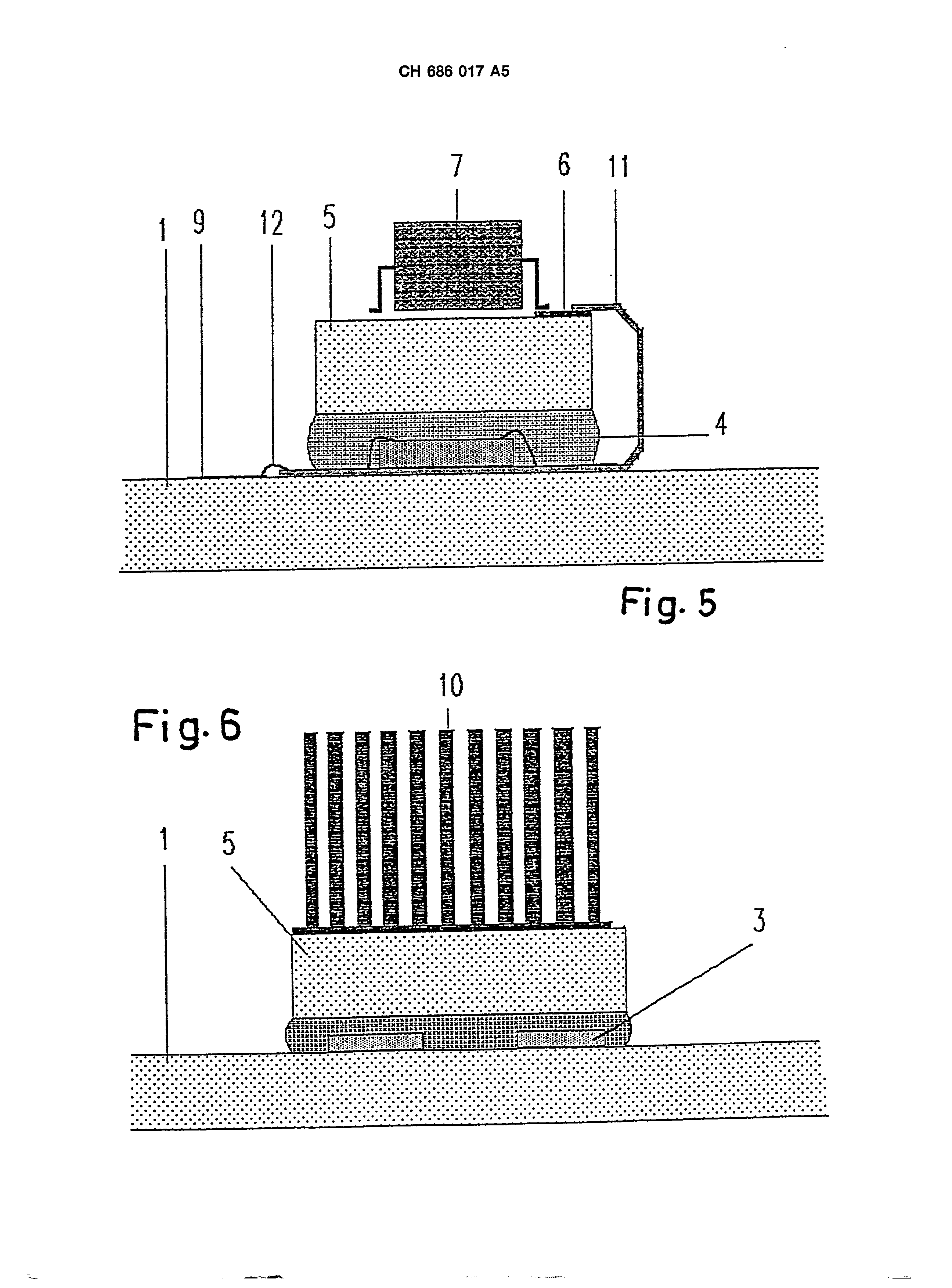
In the case of a ceramic substrate, which serves as basis of elner Diokfilmschaltung, the cover can exist likewise of the same ceramic(s) material and at the same time as substrate for a further thick film circuit, i.e. than component carriers are used. The necessary electrical connections between the basis substrate and cover egg electronics can be guaranteed by springy connection legs, which ensure at the same time that the cover parallel on the masking compound mount. Such an arrangement is in Fig. it equips 4 represented, whereby the cover 5, this time as auxiliary substrate trained, carries again conductive strips and resistances 6 if necessary and coated with further, for example, components 7 ist.
One in Fig. 4 only schematically represented connection structure 8 provides for the electrical connection of the conductive strip level 6 of the auxiliary substrate with the conductive strip level 9 of the Hauptsubstrats.
Another variant of such an arrangement is in Fig. 5 represented, with that the connection between the two conductive strip levels by a conductive strip foil 11, for example from PP with Gu-conductive strips, is realized, which is up-laminated on the substrate 1 and as carriers and connecting level of the chips serves. The connection of the Leiter3 CH 686,017 A5 4 course-even 6 and 9 takes place by means of it that it is electrically connected with these conductive strip levels either by solder contacts, for example with the conductive strip 6, or through Wire bonding, for example with the conductive strip level 9, in accordance with Fig. by the fact 5 for example that the electrical connections by the conductive strip foil under the chips accomplished werden.
Instead of forming a second electronics carrier level, the cover 5 can, as in Fig. 6 represented, also as an additional heat dissipation element trained its, by with cooling lamellas or a radiator box providing 10 ist.
A further possibility exists in accordance with Fig. 7 therein, the cover 5, e.g. with a gitterförmigen or continuous metallization 13 and if necessary also the substrate with an identical on its upper or, as in Fig. 7 represented, lower side too provides, in order to design the arrangement as Faraday cage, so that prevents electrical scattering fields and/or electromagnetic interference werden.
During the arrangement in accordance with Fig. 4 is by the connection structure 8 a suitable dissociation of the cover given, which has however a sufficient large spring action, thus the cover by the wetting with the masking compound on this “swim” kann.
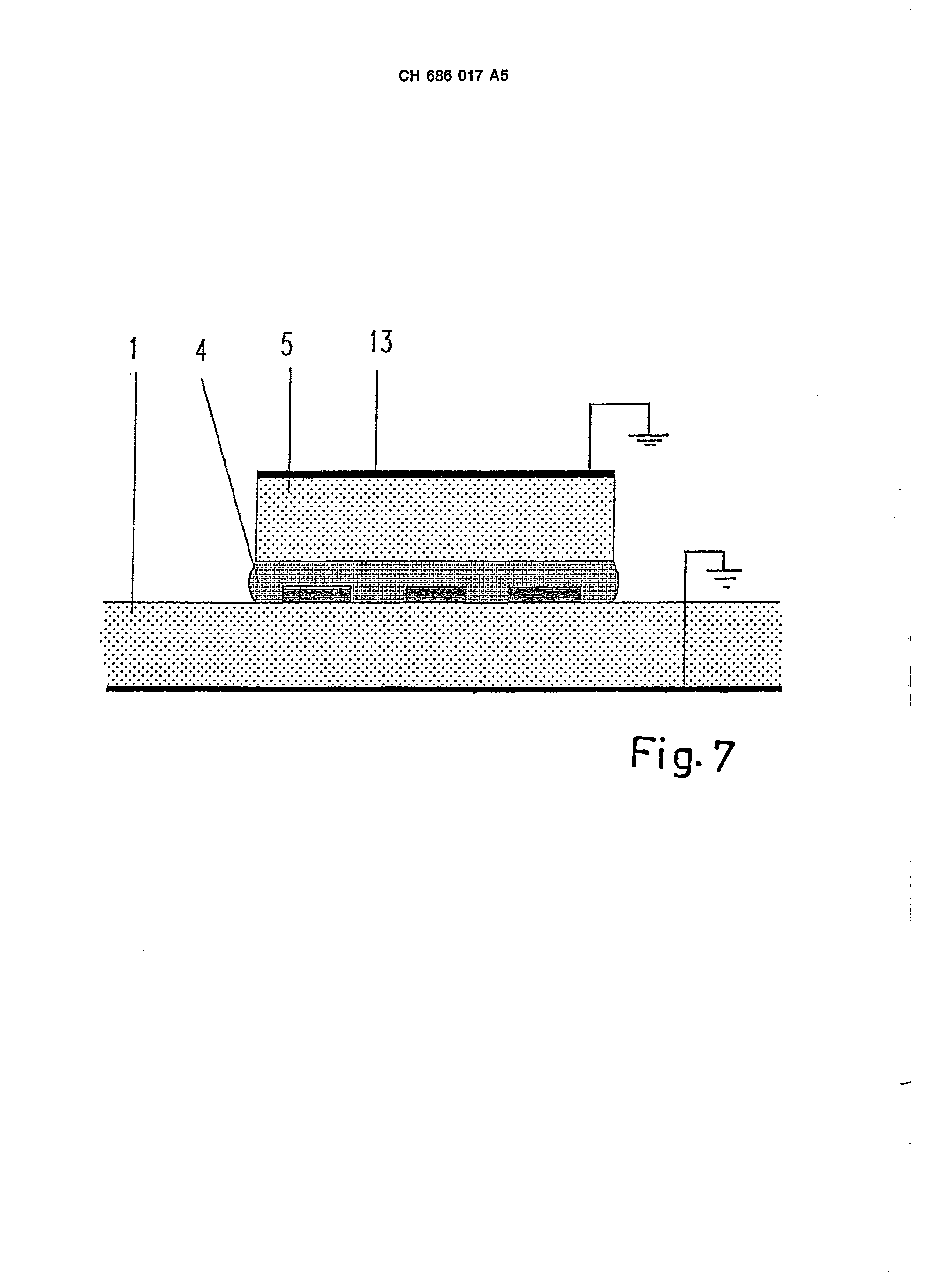
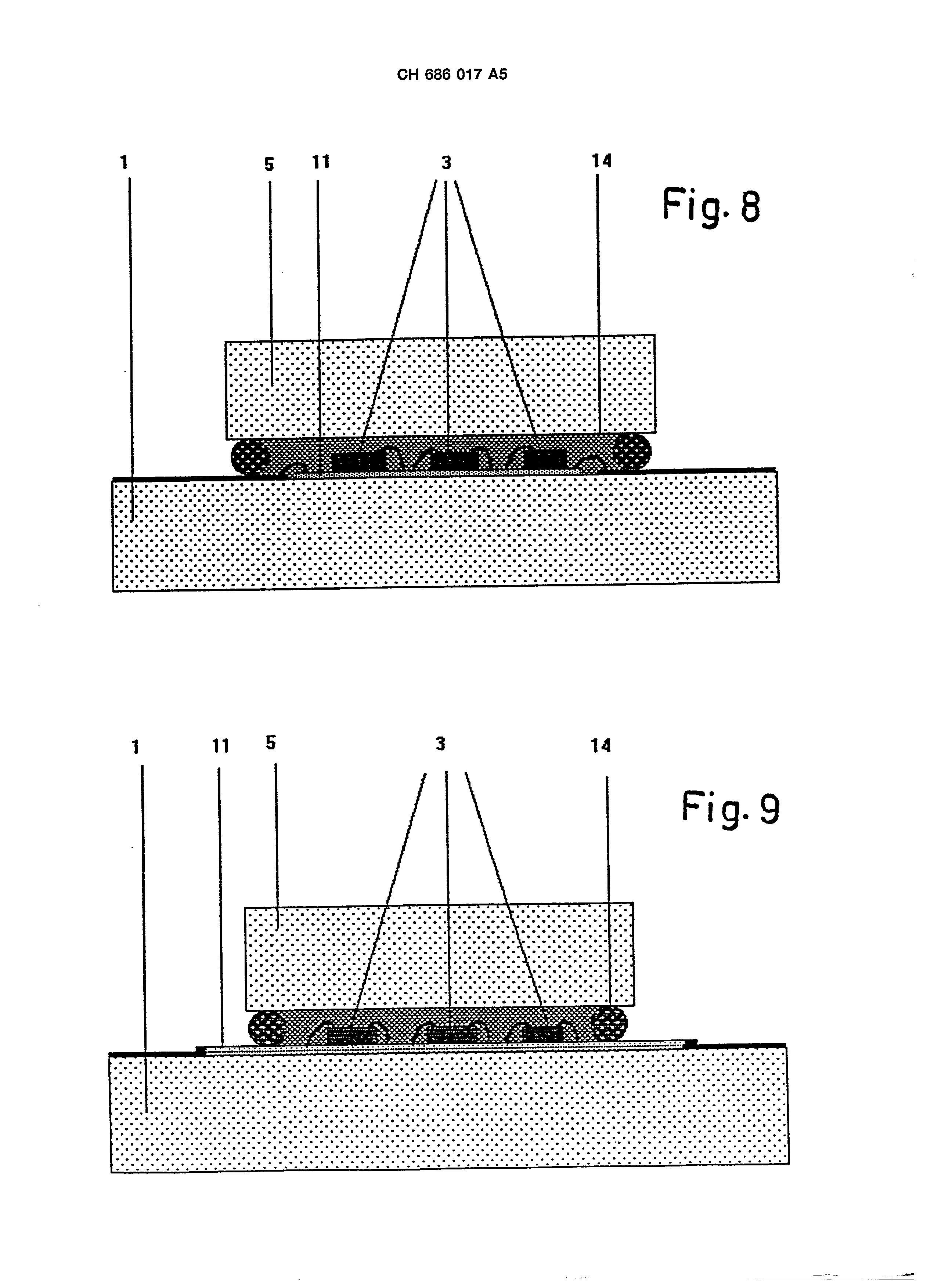
The Fig. 8 and 9 shows another possibility of reaching this by use of a prefabricated framework 14 from india rubber, silicone or another flexible material, which serve the masking compound as lateral delimitation and as distance owner between the substrate 1 and the cover 5. The case is shown that one, e.g.
from the foil substrate existing Multichip lnsel 11, on which the chips 3 are installed and bonded, completely by the framework, which is designed as Toroid ring e.g., enclosed is. By an exact dosage of the masking compound kanri to be guaranteed that the gap between substrate and cover is filled perfectly with this masking compound. The electrical connection between Multichip lnsel and the remainder of the substrate can e.g. in accordance with Fig. 8 through Wire bonding of the island metallization on the substrate metallization or in accordance with Fig. 9 by solder joints between island metallization and substrate metallization erfolgen.
As examples of the used materials and the appropriate Wärme-Ausdehnungskoeffizienten (in 10-6/°K) are mentioned:
for the cover: Epoxy 20-25 or silicone approx. for the chip: Silicon 4 for the substrate: Ceramic(s) 6,7 or print (FR4) 17-18 the cover 5 can preferably more plattenoder disk-shaped trained sein.
The metallization 9 (Fig. 1) can be with print substrates a copper laminate. The arrangement consists of a substrate and at least one chip which is embedded in a covering mass. A cover (5) is arranged on the free surface of the covering mass (4), which cover has a coefficient of thermal expansion similar to the substrate. The cover can be designed as a support and connection plane for other components (7), as electromagnetic screening or as a cooling element. The parallelism between the substrate and the cover can be guaranteed, in the embodiment with the cover as a component support, by a connecting structure (8) or, when using a preformed elastic frame as a lateral boundary for the covering mass, it can actually be guaranteed by this frame. <IMAGE> a chip, which is embedded in a masking compound, by the fact characterized that at the free surface of the masking compound (4) a cover is arranged, which exhibits a similar Wärmeausdehnungskoeffizienten as the substrate. 2. Arrangement according to requirement 1, by the fact characterized that the cover (5) by a connecting structure (8) with the substrate (1) is connected. 3. Arrangement according to requirement 2, by the fact characterized that the cover (5) as Hiltssubstrat trained, with conductive strips provides and with at least one component (7) is equipped. 4. Arrangement according to requirement 3, by the fact characterized that the connecting structure (8) at the same time as an electrically leading connection structure for those at least one component (7) dient.
Arrangement according to requirement 2, by the fact characterized that the connecting structure covers at least one conductive strip foil (11). 6. Arrangement according to requirement 5, by the fact characterized that those at least one conductive strip foil (11) under the chip (3) is led. 7. Arrangement after one of the requirements 2 to 6, by the fact characterized that the connecting structure to hold (8) as mounting plate serves at the same time, in order the cover (5) in a pre-determined distance parallel to the substrate (1). 8. Arrangement after one of the requirements 1 to 7, by the fact characterized that the cover (5) a heat dissipation element (10) carries. 9. Arrangement after one of the requirements 1 to 8, by the fact characterized that the cover (5) a grounded Metailisierung (13) exhibits. 10. Arrangement after one of the requirements 2 to 9, by the fact characterized that the connecting structure by a flexible ring (14) as distance owners in an educated manner ist. 1. Arrangement with a substrate and at least! ; , ii