METHOD FOR FABRICATING A DAMASCENE SELF-ALIGNED FERROELECTRIC RANDOM ACCESS MEMORY (F-RAM) DEVICE STRUCTURE EMPLOYING REDUCED PROCESSING STEPS
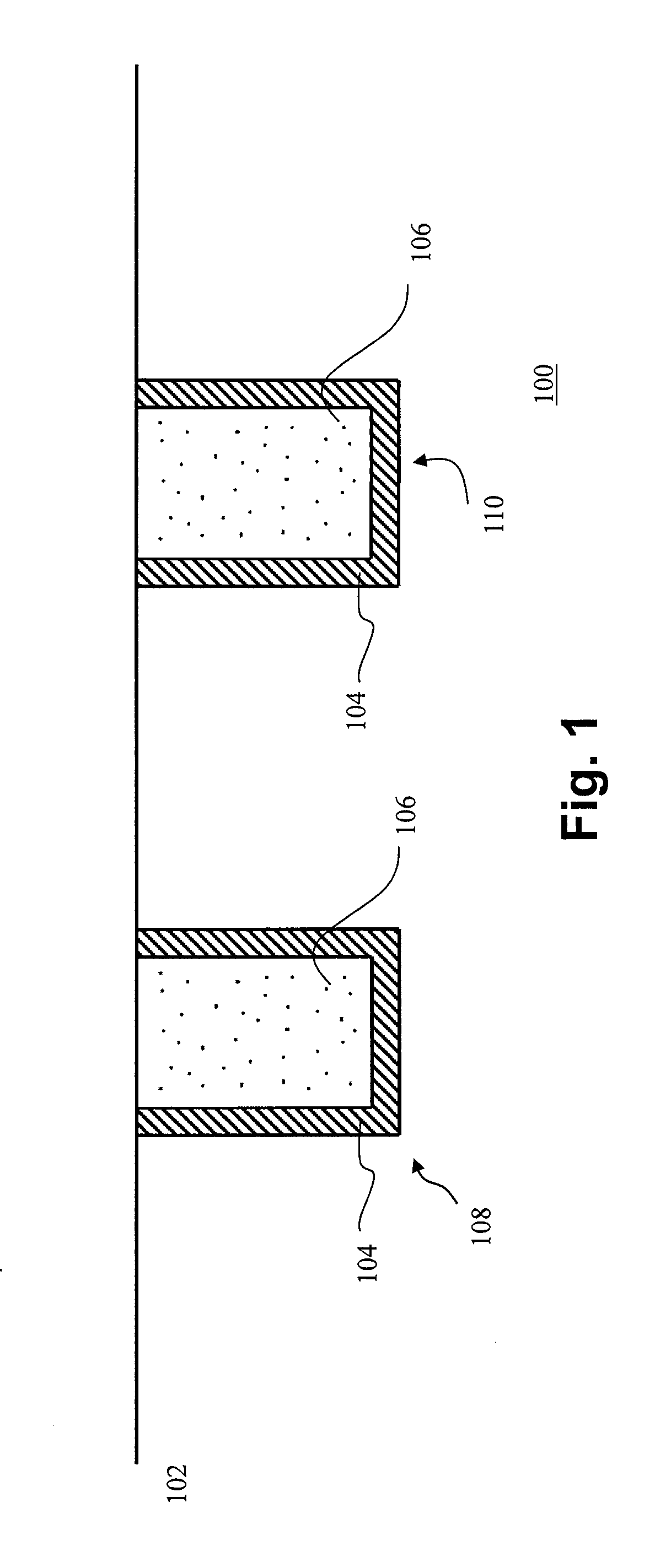
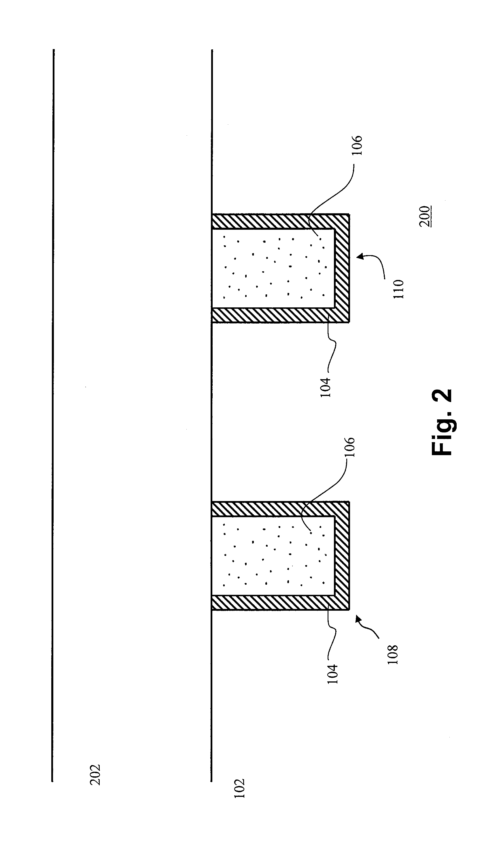
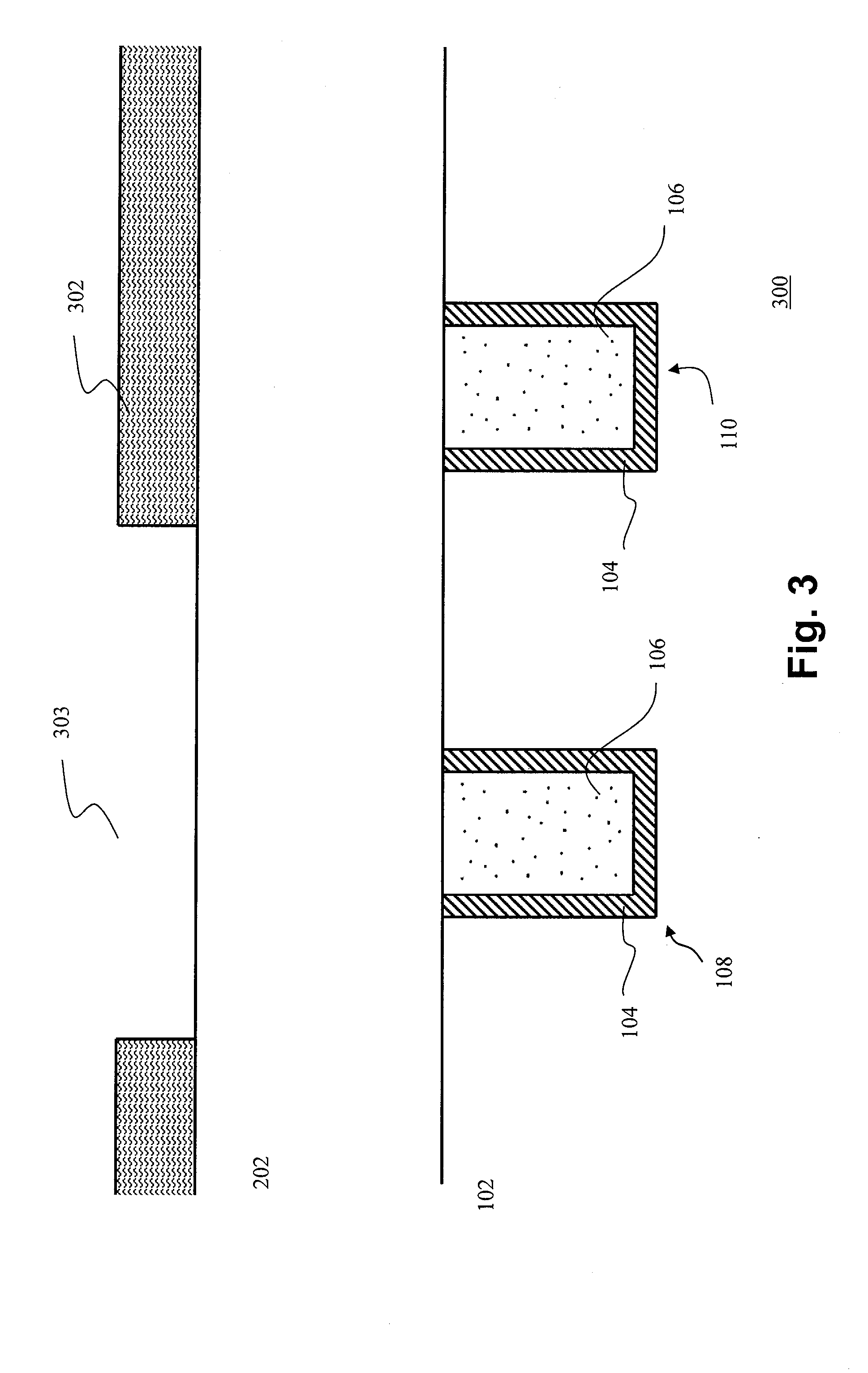
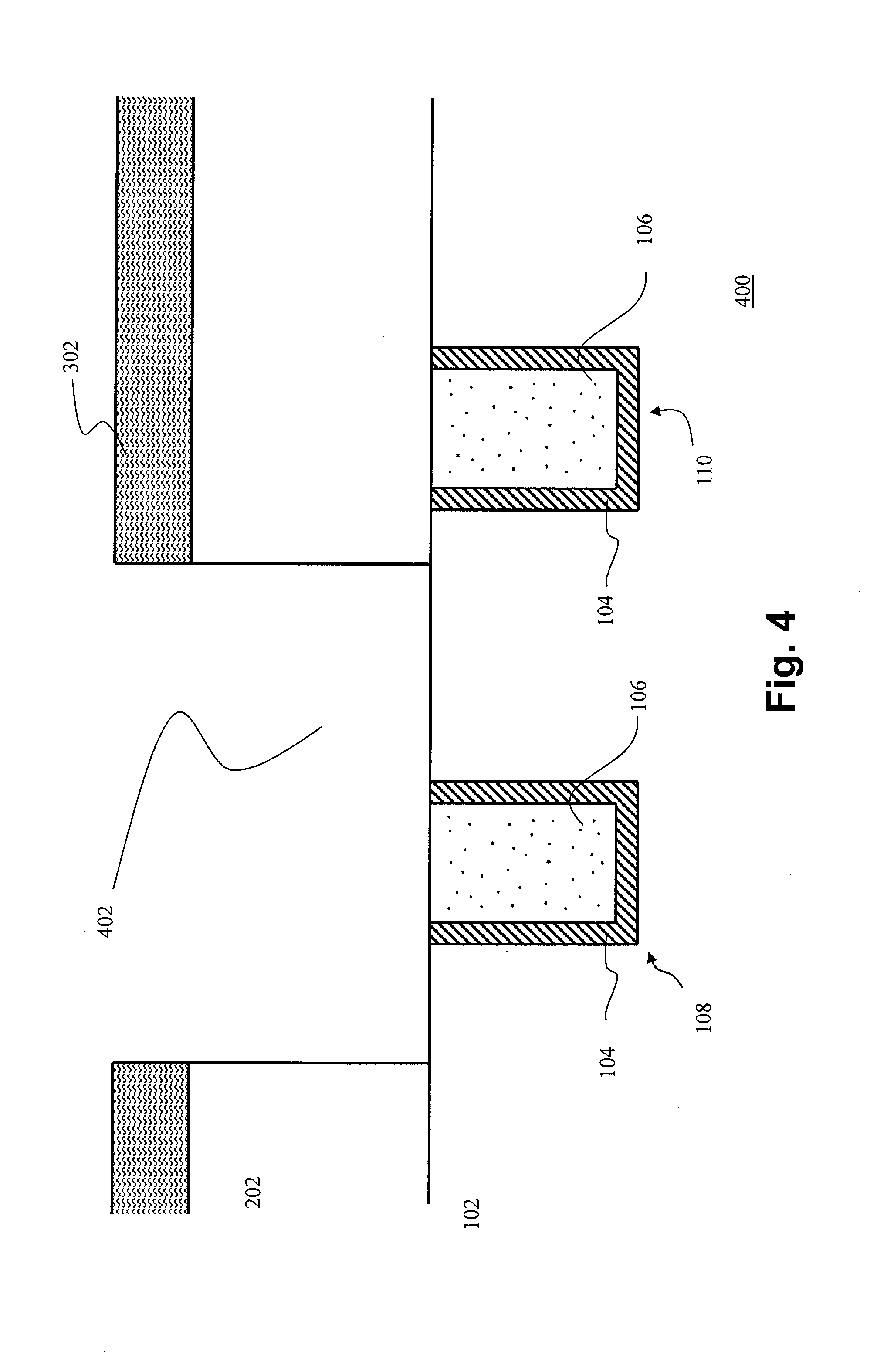
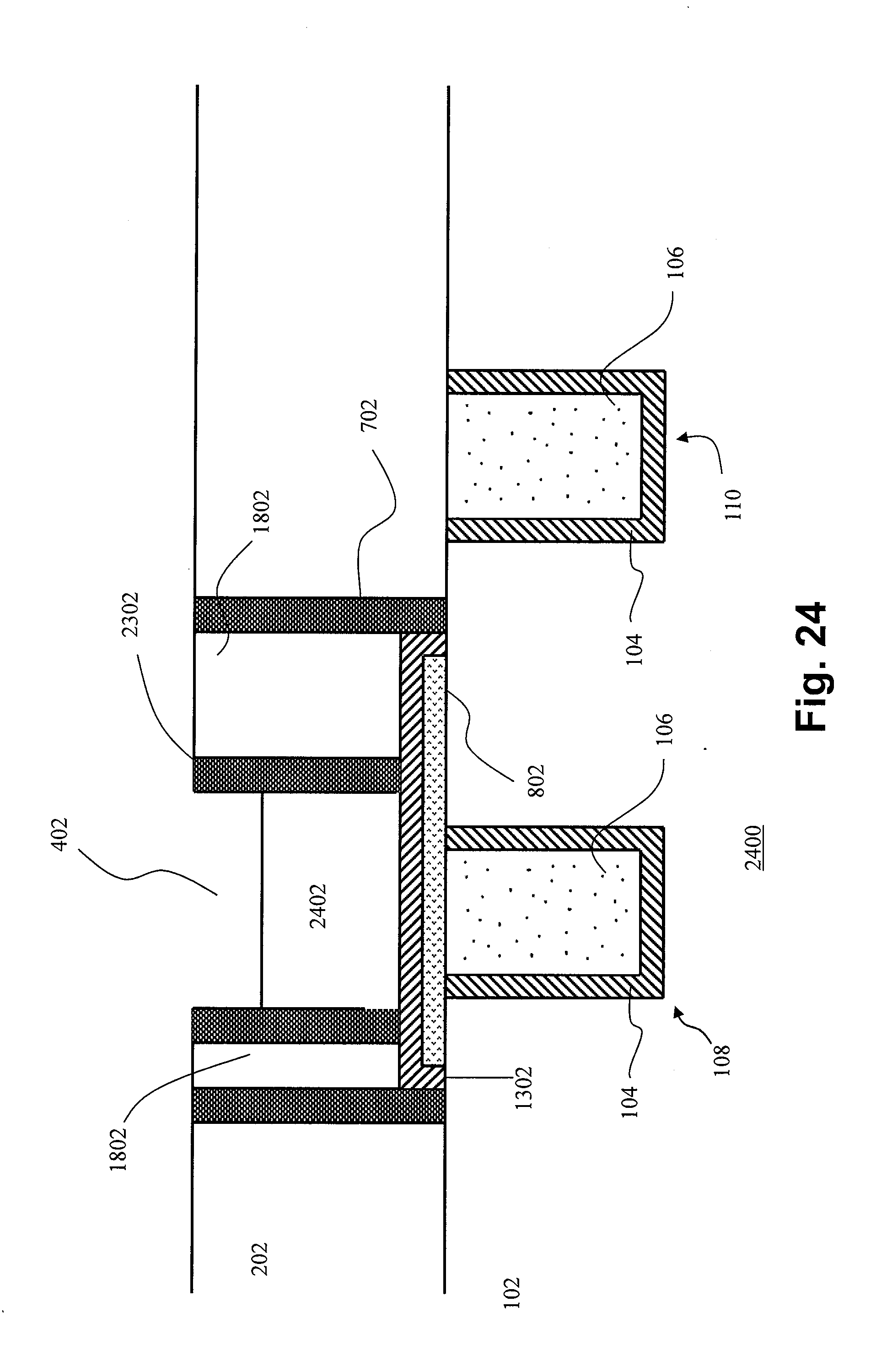
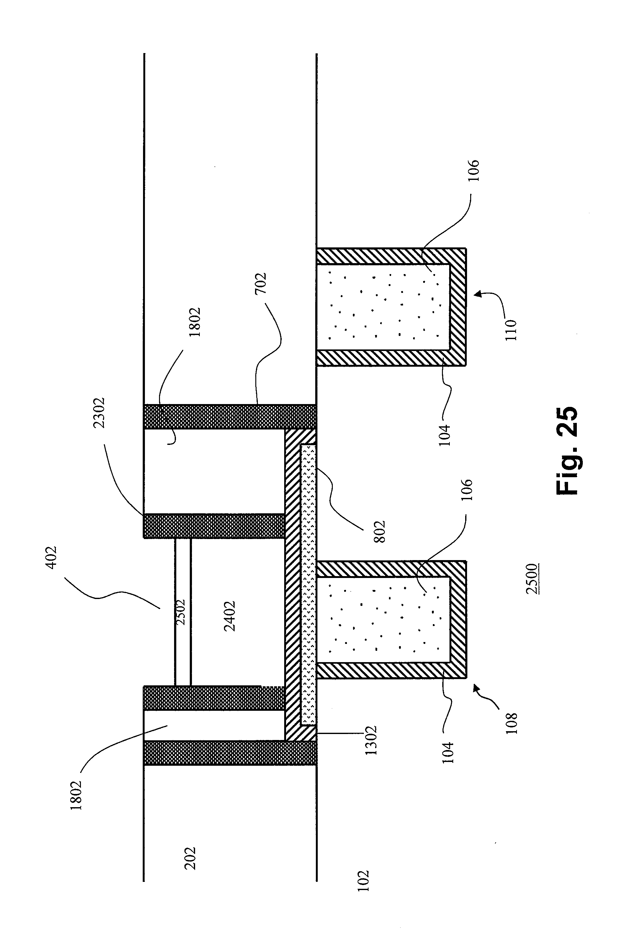
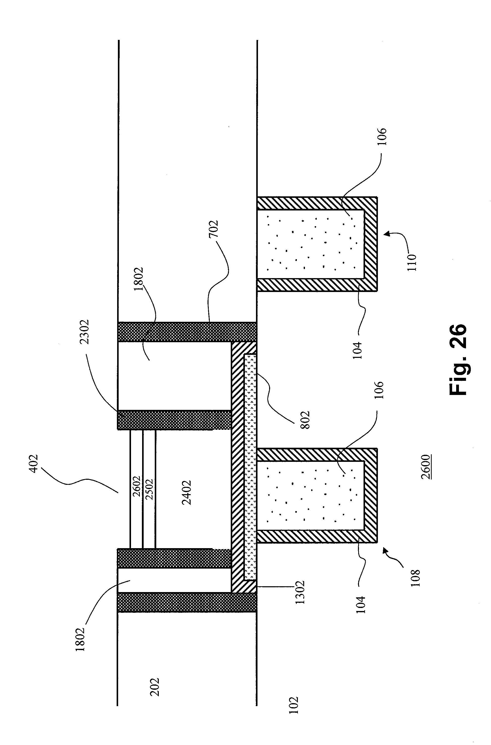
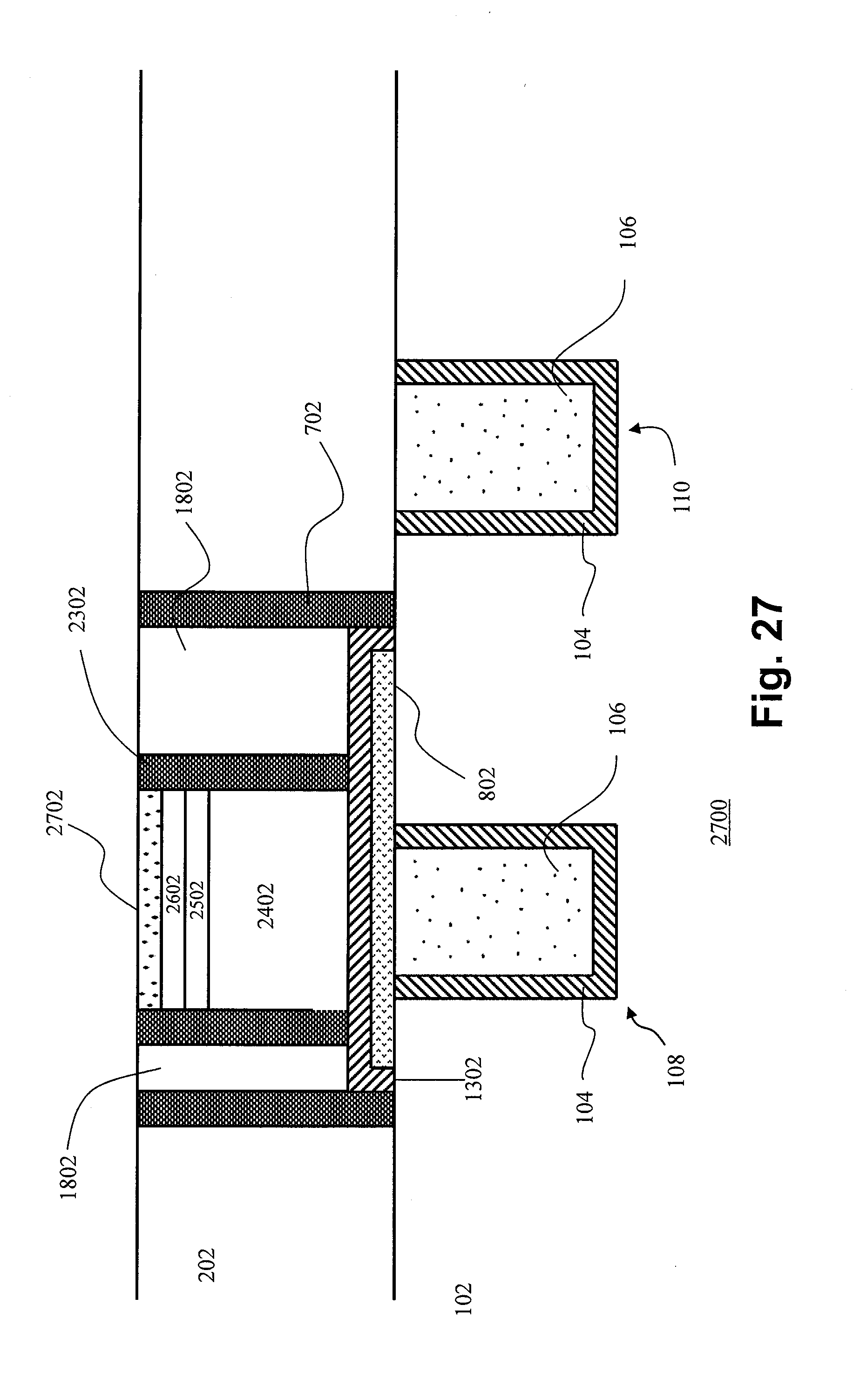
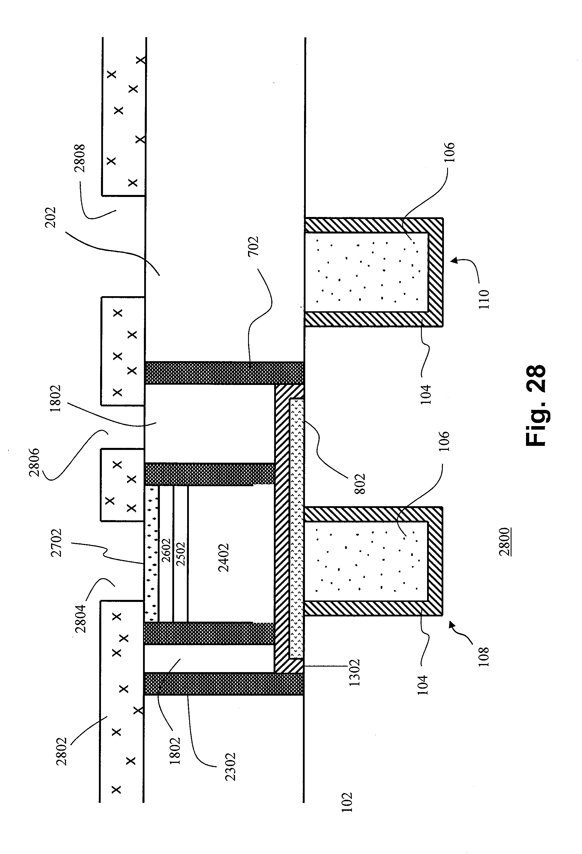
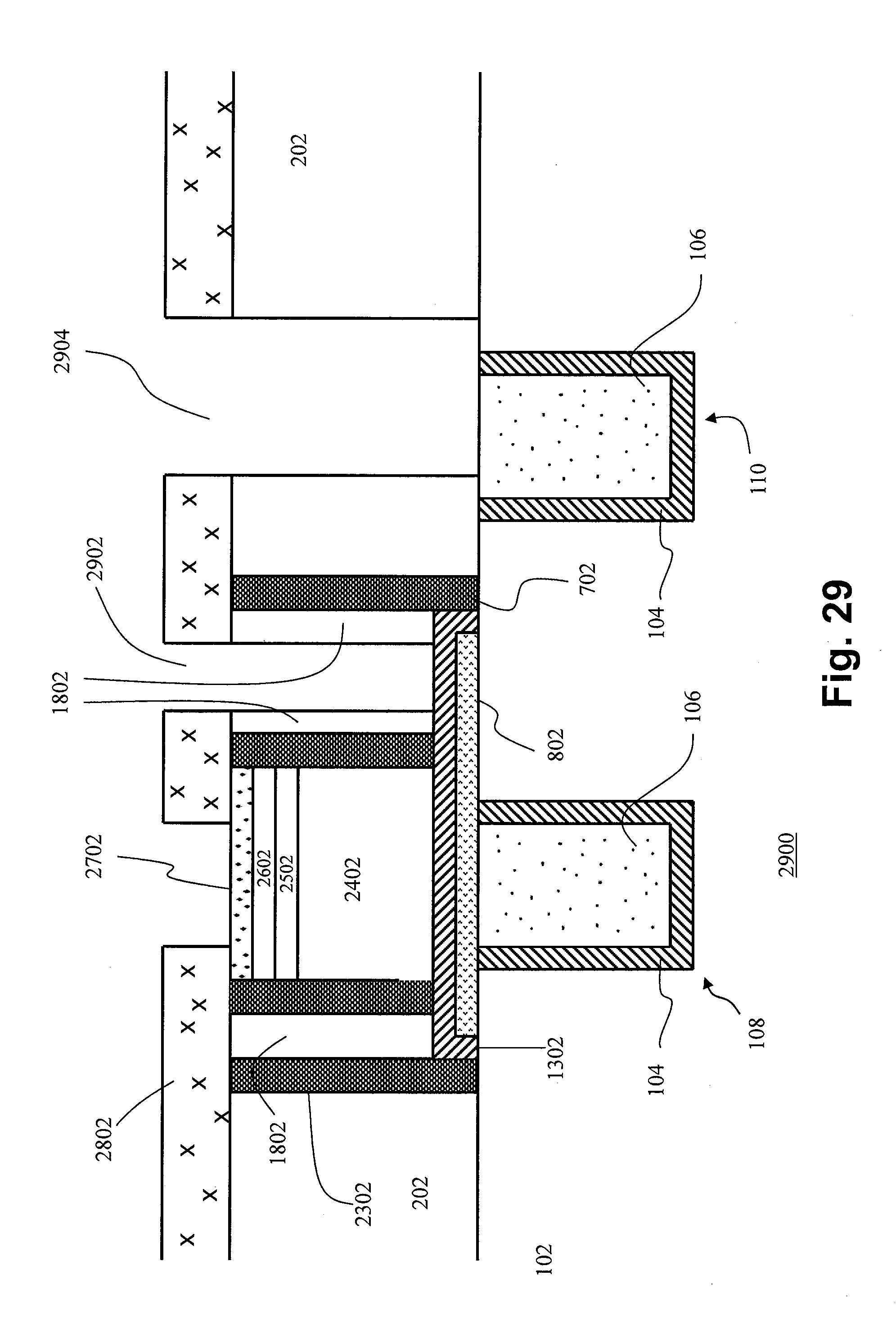
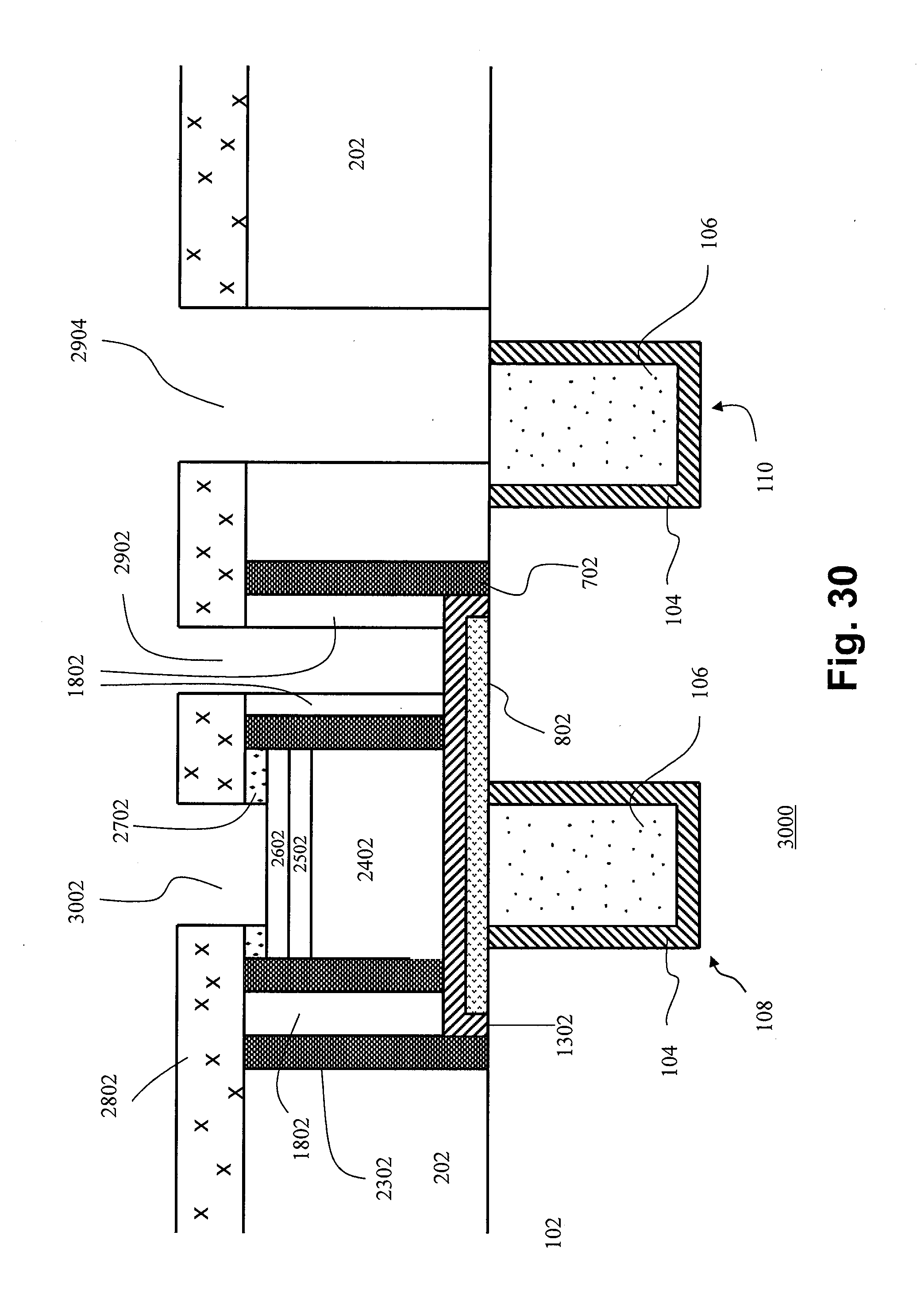
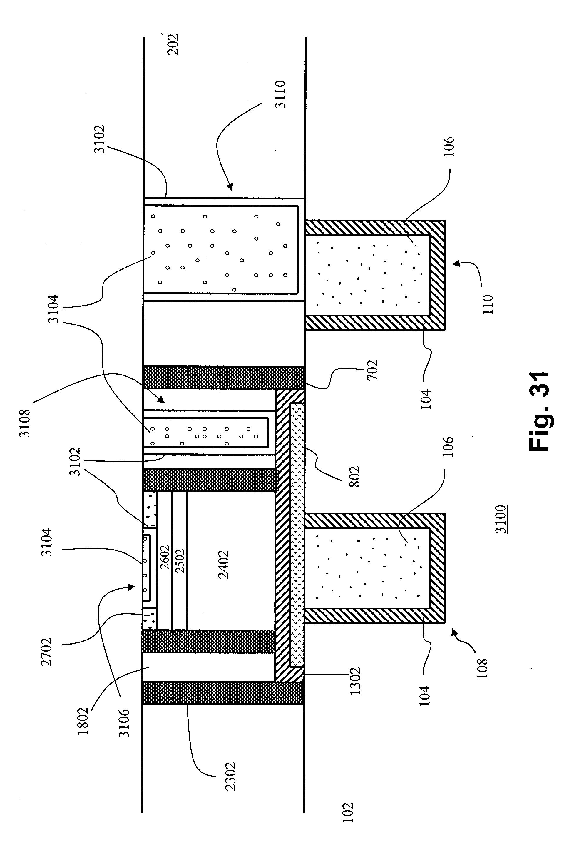
The present application claims priority from U.S. Provisional Patent Application Ser. No. 61/522,953 filed Aug. 12, 2011, the disclosure of which is herein specifically incorporated by this reference in its entirety. The present invention is also related to the subject matter disclosed in U.S. patent application Serial Nos. [RAM 627] for “Method for Fabricating a Damascene Self-Aligned Ferroelectric Random Access Memory (F-RAM) with Simultaneous Formation of Sidewall Ferroelectric Capacitors” and [RAM 628] for “Method for Fabricating a Damascene Self-Aligned Ferroelectric Random Access Memory (F-RAM) Having a Ferroelectric Capacitor Aligned with a Three Dimensional Transistor structure”, both filed on even date herewith and assigned to Ramtron International Corporation, the disclosures of which are also herein specifically incorporated by this reference in their entirety. The present invention relates, in general, to the field of integrated circuit (IC) memory devices. More particularly, the present invention relates to the field of non-volatile, ferroelectric random access memory (F-RAM) devices and a method for fabricating a damascene self-aligned F-RAM device structure on a planar surface using a reduced number of masks and etching steps. According to World Semiconductor Trade Statistics (WSTS), the semiconductor market reached an important milestone in 2010, posting worldwide revenues of more than $300 billion (in United States dollars) for the first time in the industry's history. In particular, the memory chip segment exhibited the highest growth rate during 2010, increasing from $45 billion in 2009 to $71 billion in 2010, representing a 57% year-over-year growth rate. Embedded memory devices represented more than 23% of the overall semiconductor market in 2010. Within this context, the increasing demand for higher processing power is driving the semiconductor industry to develop memory devices with higher operational speeds in order to support the capabilities of modern electronic devices. F-RAM has emerged as a promising option for the industry, particularly in the market areas of mobile computing, smart meters, radio frequency identification (RFID) devices, office equipment and other applications requiring non-volatile data storage. Standard dynamic random access memory (DRAM) and static random access memory (SRAM) devices, while providing relatively fast access times, are considered to be volatile memory devices inasmuch as data stored in such memories is lost when power is interrupted. In contrast, non-volatile memory devices are those that function to retain data despite any loss of power. F-RAM devices are inherently non-volatile, meaning that these memory devices are able to retain stored data while the device is not powered. In comparison to electrically erasable programmable read only memory (EEPROM) FLASH memory devices, which are currently the most popular type of non-volatile memory, F-RAM devices have several advantages including lower power requirements (operational voltages of just 5V needed during read-write operations), higher read-write speeds (less than 70 nanoseconds), and virtually unlimited write endurance capability (more than 10,000,000,000 write cycles). F-RAM memory devices may be fabricated based on the use of lead zirconium titanate (PZT) ferroelectric storage capacitors as memory elements integrated with complementary metal oxide semiconductor (CMOS) addressing, selection, and control logic. PLZT is a lanthanum-doped form of PZT wherein some of the lead is replaced with Lanthanum. It is also known that PZT may also be doped with strontium and calcium to improve its ferroelectric dielectric properties. Ferroelectric storage capacitors having a strontium bismuth tantalate (SBT); barium strontium titanate (BST); and strontium titanate oxide (STO) dielectrics are also known in the art. As used in the present application, the term “PZT” shall also be considered to include PLZT, SBT, BST, STO and other comparable ferroelectric dielectric materials. Further, it should be noted that the techniques of the present invention disclosed herein are applicable to all known ferroelectric dielectrics including Perovskites and layered Perovskites (whether doped or undoped) including PZT, PLZT, BST, SBT, STO and others while simultaneously allowing for a potentially broader choice of electrode materials and the use of a forming gas anneal process step on the completed IC structure. Regardless of the ferroelectric dielectric material employed, in operation F-RAM devices function through their ability to be polarized in one direction or another in order to store a binary value representative of a logic level “one” or “zero”. The ferroelectric effect allows for the retention of a stable polarization state in the absence of an applied electric field due to the alignment of internal dipoles within the Perovskite crystals in the dielectric material. This alignment may be selectively achieved by application of an electric field which exceeds the coercive field of the material. Conversely, reversal of the applied field reverses the internal dipoles. A hysteresis curve, wherein the abscissa and ordinate represent the applied voltage (“V”) and resulting polarization (“Q”) states respectively, may be plotted to represent the response of the polarization of a ferroelectric capacitor to the applied voltage. A more complete description of this characteristic hysteresis curve is disclosed, for example, in U.S. Pat. Nos. 4,914,627 and 4,888,733 assigned to Ramtron International Corporation, assignee of the present invention, the disclosures of which are herein specifically incorporated by this reference. Representative of the current state of the art in F-RAM device fabrication is that disclosed in U.S. Pat. No. 6,150,184 for: “Method of Fabricating Partially or Completely Encapsulated Top Electrode of a Ferroelectric Capacitor,” also assigned to Ramtron International Corporation. Therein described is the structure of a ferroelectric capacitor that includes a bottom electrode, a top electrode, and a ferroelectric layer located between the top and bottom electrodes that extends to completely encapsulate the top electrode, except for a contact hole to allow metallization of the top electrode. The total encapsulation of the top electrode reduces the sensitivity of the ferroelectric capacitor to hydrogen and thus improves electrical switching performance. The encapsulation technique can also be used to improve the performance of ferroelectric integrated circuits and other devices. Further representative of the state of the art in the fabrication of F-RAM devices is that disclosed in U.S. Pat. No. 6,613,586 for: “Hydrogen Barrier Encapsulation Techniques for the Control of Hydrogen Induced Degradation of Ferroelectric Capacitors in Conjunction with Multilevel Metal Processing for Non-Volatile Integrated Circuit Memory Devices,” also assigned to Ramtron International Corporation. Therein described is a device structure which ameliorates the hydrogen induced degradation of ferroelectric capacitors by completely encapsulating the capacitor within a suitable hydrogen barrier material, such as chemical vapor deposition (“CVD”) or sputtered silicon nitride (Si3N4), thus ensuring process compatibility with industry standard process steps. Although the deposition process for CVD Si3N4itself contains hydrogen, the deposition time may be kept relatively short thereby allowing the titanium nitride (TiN) local interconnect layer to act as a “short term” hydrogen barrier. The disclosures of U.S. Pat. Nos. 6,150,184 and 6,613,586 are herein specifically incorporated by this reference in their entirety. Despite the aforementioned advantages over volatile memory devices and other non-volatile technologies, F-RAMs currently account for a relatively small share of the non-volatile memory device market. Competitively, the main limitation of the F-RAM technology has been its lower storage density compared to FLASH devices coupled with higher manufacturing costs. These limitations stem primarily from the generally complex structure of current F-RAM devices which results in a manufacturing process that requires a high number of processing masks and etching steps. As such, in order to be more competitive in the current memory device marketplace and be usable in a wider range of modern electronic devices, F-RAM devices need to be more highly integrated, implying increased storage densities and reduced manufacturing costs. As such, it would be highly advantageous to reduce the number of layers and etching steps required during F-RAM fabrication in order to reduce manufacturing costs. Still further, it would be highly advantageous to simplify the structure of F-RAM devices with the purpose of improving storage density capabilities. Disclosed herein is a method for forming a damascene self-aligned ferroelectric RAM (F-RAM) device on a planar surface comprising the steps of forming, on a planar surface of a semiconductor substrate, a thick oxide layer which is etched based on the pattern established by a non-erodible mask, forming an opening for the F-RAM construction, followed by the application and etching of a CVD aluminum oxide conformal layer to form spacers, deposition of a titanium aluminum nitride layer, followed by the application and O2plasma ash etching of a photoresist material, deposition and planarization of an oxide material using chemical mechanical polishing (CMP), application of a photoresist mask to create an etching pattern on the oxide, deposition of a CVD aluminum oxide conformal layer to form a second set of spacers after the oxide is etched, deposition, planarization and etching of a ferroelectric layer ideally doped with lead zirconium titanate (PZT), followed by a similar process on top electrode and nitride layers, and the etching of the oxide and nitride layers for the formation of CVD tungsten, titanium/titanium nitride studs on a planar surface of the F-RAM structure. Also further disclosed herein is a method for forming an integrated circuit device on a substrate comprising forming a first insulating layer on the substrate and removing a portion of the first insulating layer to produce an opening to an exposed surface of the substrate therein. First spacers are formed on sidewalls of the opening and a first conductive layer is formed on the exposed surface of the substrate separated from the first spacers on the sidewalls of the opening by a gap therebetween. A bottom electrode of a ferroelectric capacitor is formed over the first conductive layer and in the gap laterally of the first conductive layer. A second insulating layer is formed adjoining the spacers in the opening and second spacers are formed on the second insulating layer in the opening. A ferroelectric dielectric layer is formed on the bottom electrode between the second spacers and a top electrode is formed on the ferroelectric dielectric. A bottom electrode contact opening is formed through a portion of the second insulating layer to the bottom electrode and a first electrical contact is formed to the top electrode and a second electrical contact is formed to the bottom electrode through the bottom electrode contact opening. Still further disclosed herein is a method for forming a ferroelectric device on a planar surface of a semiconductor substrate comprising forming a relatively thick oxide layer on the planar surface and selectively etching an opening through the oxide layer in a pattern established by a non-erodible mask. A first aluminum oxide conformal layer is applied and selectively etched to form first spacers on sidewalls of the opening and a titanium aluminum nitride layer is deposited in a lower portion of the opening and separated from the first spacers. A bottom electrode of a ferroelectric capacitor is formed over the aluminum oxide layer in contact with the spacers and laterally of the aluminum oxide layer. An oxide material is deposited, planarized and selectively removed to form an additional oxide layer adjoining the first spacers in the opening. A second aluminum oxide layer is deposited and selectively etched to form second spacers on the additional oxide layer. A ferroelectric layer is deposited and etched on the bottom electrode between the second spacers. A top electrode is formed on the ferroelectric layer and a Ti/TiN and W contact is formed to the bottom electrode through the oxide material and a Ti/TiN and W contact is also substantially concurrently formed to the top electrode. Additionally disclosed herein is a ferroelectric device which comprises a contact stud formed upon a semiconductor substrate and a first conductive layer overlying the substrate and adjoining the contact stud. A bottom electrode layer overlies the first conductive layer and first spacers are disposed laterally of the bottom electrode layer extending distally of the substrate. Second spacers are disposed on the bottom electrode layer extending distally therefrom substantially parallel to the first spacers and an insulating layer is disposed between the first and second spacers. A ferroelectric dielectric layer overlies the bottom electrode layer between the second spacers and a top electrode layer overlies the ferroelectric dielectric layer. A top electrode contact adjoins the top electrode layer and a bottom electrode contact adjoins the bottom electrode layer extending through the insulating layer. Also further disclosed herein is a method for forming an integrated circuit device on a substrate including at least one contact stud. The method comprises forming a first insulating layer on the substrate and removing a portion of the first insulating layer to produce an opening to an exposed surface of said substrate therein. First spacers are formed on the sidewalls of the opening and a first conductive layer is formed in contact with the contact stud on the exposed surface of the substrate separated from the first spacers on the sidewalls of the opening by a gap therebetween. A bottom electrode of a ferroelectric capacitor is formed over the first conductive layer and in the gap laterally of the first conductive layer. A second insulating layer is formed adjoining the spacers in the opening and second spacers are formed on the second insulating layer in the opening. A ferroelectric dielectric is formed on the bottom electrode between the second spacers and a top electrode is formed on the ferroelectric dielectric. An electrical contact is then formed to the top electrode. Also further disclosed herein is a ferroelectric device which comprises a semiconductor substrate and a first conductive layer overlying the semiconductor substrate. A bottom electrode layer overlies the first conductive layer and first spacers are disposed laterally of the bottom electrode layer and extend distally of the substrate. Second spacers are disposed on the bottom electrode layer and extend distally therefrom substantially parallel to the first spacers. An insulating layer is disposed between the first and second spacers and a ferroelectric dielectric layer overlies the bottom electrode layer between the second spacers. A top electrode layer overlies the ferroelectric dielectric layer, a top electrode contact adjoins the top electrode layer and a bottom electrode contact adjoins the bottom electrode layer extending through the insulating layer. The aforementioned and other features and objects of the present invention and the manner of attaining them will become more apparent and the invention itself will be best understood by reference to the following description of a preferred embodiment taken in conjunction with the accompanying drawings, wherein: The present invention presents a novel, non-volatile, ferroelectric random access memory (F-RAM) device and a method for fabricating a damascene self-aligned F-RAM device structure on a planar surface using a reduced number of masks and etching steps. A representative method in accordance with the present invention comprises the processing steps disclosed in With reference now to With reference additionally now to With reference additionally now to With reference additionally now to With reference additionally now to With reference additionally now to With reference additionally now to With reference additionally now to With reference additionally now to With reference additionally now to An enhanced view of section 1104 is shown (above-right) to detail the structure formed after the etching away of the titanium aluminum nitride 802 layer. Section 1104 illustrates how the titanium aluminum nitride 802 coating is etched back to the base of the thick oxide 202 layer, leaving a layer of titanium aluminum nitride 802 only below the remaining photoresist 902 material. With reference additionally now to With reference additionally now to This platinum 1302 layer covers the top and bottom of the thick oxide 202, the top of the titanium aluminum nitride 802 layer and sidewalls of the Al2O3spacers 702. With reference additionally now to With reference additionally now to With reference additionally now to With reference additionally now to With reference additionally now to With reference additionally now to With reference additionally now to With reference additionally now to With reference additionally now to With reference additionally now to With reference additionally now to With reference additionally now to With reference additionally now to With reference additionally now to With reference additionally now to With reference additionally now to With reference additionally now to With reference additionally now to The last process steps are illustrated in As can be appreciated by reference to the drawing figures, there are provided alternative contacts to the bottom electrode (platinum 1302 layer) of the ferroelectric capacitor in the form of contact stud 108 and contact stud 3108. Although both are herein illustrated and described, either may be utilized alone or in combination. It should be noted that omitting contact stud 3108 will provide greater device density in an integrated circuit embodiment of the present invention. While there have been described above the principles of the present invention in conjunction with specific processing steps and device structure, it is to be clearly understood that the foregoing description is made only by way of example and not as a limitation to the scope of the invention. Particularly, it is recognized that the teachings of the foregoing disclosure will suggest other modifications to those persons skilled in the relevant art. Such modifications may involve other features which are already known per se and which may be used instead of or in addition to features already described herein. Although claims have been formulated in this application to particular combinations of features, it should be understood that the scope of the disclosure herein also includes any novel feature or any novel combination of features disclosed either explicitly or implicitly or any generalization or modification thereof which would be apparent to persons skilled in the relevant art, whether or not such relates to the same invention as presently claimed in any claim and whether or not it mitigates any or all of the same technical problems as confronted by the present invention. The applicants hereby reserve the right to formulate new claims to such features and/or combinations of such features during the prosecution of the present application or of any further application derived therefrom. As used herein, the terms “comprises”, “comprising”, or any other variation thereof, are intended to cover a non-exclusive inclusion, such that a process, method, article, or apparatus that comprises a recitation of certain elements does not necessarily include only those elements but may include other elements not expressly recited or inherent to such process, method, article or apparatus. None of the description in the present application should be read as implying that any particular element, step, or function is an essential element which must be included in the claim scope and THE SCOPE OF THE PATENTED SUBJECT MATTER IS DEFINED ONLY BY THE CLAIMS AS ALLOWED. Moreover, none of the appended claims are intended to invoke paragraph six of 35 U.S.C. Sect. 112 unless the exact phrase “means for” is employed and is followed by a participle. Disclosed is a novel non-volatile, ferroelectric random access memory (F-RAM) device and a method for fabricating a damascene self-aligned F-RAM device structure on a planar surface using a reduced number of masks and etching steps. 1. A method for forming an integrated circuit device on a substrate comprising:
forming a first insulating layer on said substrate; removing a portion of said first insulating layer to produce an opening to an exposed surface of said substrate therein; forming first spacers on sidewalls of said opening; forming a first conductive layer on said exposed surface of said substrate separated from said first spacers on said sidewalls of said opening by a gap therebetween; forming a bottom electrode of a ferroelectric capacitor over said first conductive layer and in said gap laterally of said first conductive layer; forming a second insulating layer adjoining said spacers in said opening; forming second spacers on said second insulating layer in said opening; forming a ferroelectric dielectric on said bottom electrode between said second spacers; forming a top electrode on said ferroelectric dielectric; forming a bottom electrode contact opening through a portion of said second insulating layer to said bottom electrode; and forming a first electrical contact to said top electrode and a second electrical contact to said bottom electrode through said bottom electrode contact opening. 2. The method of providing at least one contact stud in said substrate extending to said exposed surface of said substrate in said opening. 3. The method of depositing a first spacer material over said first insulating layer; and removing said first spacer material except on said sidewalls of said opening. 4. The method of 5. The method of 6. The method of depositing a first conductive layer material over said first insulating layer and said first spacers; and removing said first conductive layer material except on said exposed surface of said substrate separated from said first spacers by said gap. 7. The method of 8. The method of 9. The method of depositing a bottom electrode material over said first insulating layer, said first spacers and in said gap laterally of said first, conductive layer in said opening; and removing said bottom electrode material except over said bottom electrode and within said gap. 10. The method of 11. The method of 12. The method of depositing an oxide over said first insulating layer, said first spacers and said bottom electrode; and removing said oxide except adjoining said first spacers. 13. The method of depositing a second spacer material over said first and second insulating layers and said bottom electrode; and removing said second spacer material except adjoining said second insulting layer in said opening. 14. The method of 15. The method of 16. The method of depositing said ferroelectric dielectric material over said bottom electrode; and annealing said ferroelectric dielectric material. 17. The method of 18. The method of depositing a top electrode material over said ferroelectric dielectric. 19. The method of 20. The method of forming a contact layer material over said top electrode. 21. The method of 22. The method of anisotropically etching said portion of said second insulating layer to said bottom electrode. 23. The method of depositing a conductive layer material over said top electrode and said bottom electrode in said bottom electrode contact opening. 24. The method of firstly depositing a first contact material over said top electrode and said bottom electrode adjoining sidewalls of said bottom electrode contact opening; and secondly depositing said conductive layer material over said first contact material. 25. The method of 26. The method of 27. A method for forming a ferroelectric device on a planar surface of a semiconductor substrate comprising:
forming a relatively thick oxide layer on said planar surface; selectively etching an opening through said oxide layer in a pattern established by a non-erodible mask; applying and selectively etching a first aluminum oxide conformal layer to form first spacers on sidewalls of said opening; depositing a titanium aluminum nitride layer in a lower portion of said opening and separated from said first spacers; forming a bottom electrode of a ferroelectric capacitor over said first aluminum oxide conformal layer and in contact with said spacers laterally of said first aluminum oxide conformal layer; depositing, planarizing and selectively removing an oxide material to form an additional oxide layer adjoining said first spacers in said opening; depositing and selectively etching a second aluminum oxide layer to form second spacers on said additional oxide layer; depositing and etching a ferroelectric layer on said bottom electrode between said second spacers; forming a top electrode on said ferroelectric layer; forming a Ti/TiN and W contact to said bottom electrode through said oxide material; and also substantially concurrently forming a Ti/TiN and W contact to said top electrode. 28. The method of 29. The method of chemical vapor deposition of aluminum oxide over said relatively thick oxide layer and within said opening; and removal of said aluminum oxide from said relatively thick oxide layer and the planar surface of said substrate leaving said first spacers. 30. The method of 31. The method of chemical vapor deposition of titanium aluminum nitride over said relatively thick oxide layer and within said opening; and removal of said titanium aluminum nitride from said relatively thick oxide layer and said first spacers. 32. The method of 33. The method of depositing a noble metal over said relatively thick oxide layer, said first spacers and said titanium aluminum nitride layer; and removing said noble metal from said relatively thick oxide layer and said first spacers except for over said titanium aluminum nitride layer and laterally thereof in contact with said first spacers. 34. The method of 35. The method of 36. The method of depositing said oxide material over said relatively thick oxide layer, said first spacers and said bottom electrode in said opening; chemical mechanical polishing of said oxide material to a level of said first spacers; and removing said oxide material within said opening to a level of said bottom electrode except adjoining said first spacers to form said additional oxide layer adjoining said first spacers. 37. The method of chemical vapor deposition of aluminum oxide over said relatively thick oxide layer, said additional oxide layer adjoining said first spacers and said bottom electrode; and removal of said aluminum oxide from said relatively thick oxide layer and upper portions of said additional oxide material and said bottom electrode to form said second spacers medially displaced from said first spacers. 38. The method of 39. The method of depositing a ferroelectric material on said bottom electrode between said second spacers; and removing a portion of said ferroelectric material to a level below distal ends of said second spacers. 40. The method of 41. The method of depositing a noble metal over said ferroelectric layer; and etching said noble metal to a level below distal ends of said second spacers. 42. The method of 43. The method of also depositing a Ti/TIN layer over said noble metal; and etching said Ti/TiN layer to a level below distal ends of said second spacers. 44. The method of depositing a nitride layer over said top electrode; planarizing said nitride layer to a level of said relatively thick oxide layer; etching through a portion of said additional oxide layer to form a bottom electrode contact opening; and etching through said nitride layer to form a top electrode contact opening. 45. The method of depositing Ti/TiN liners in said bottom electrode contact opening and said top electrode contact opening; and chemical vapor depositing W in said Ti/TiN liners. 46. The method of planarizing said contacts to said bottom and top electrodes to a level of said relatively thick oxide layer. 47. The method of 48. A ferroelectric device comprising:
a contact stud formed upon a semiconductor substrate; a first conductive layer overlying said semiconductor substrate and adjoining said contact stud; a bottom electrode layer overlying said first conductive layer; first spacers disposed laterally of said bottom electrode layer extending distally of said substrate; second spacers disposed on said bottom electrode layer extending distally therefrom substantially parallel to said first spacers; an insulating layer disposed between said first and second spacers; a ferroelectric dielectric layer overlying said bottom electrode layer between said second spacers; a top electrode layer overlying said ferroelectric dielectric layer; and a top electrode contact adjoining said top electrode layer, said contact stud forming a bottom electrode contact. 49. The ferroelectric device of a Ti/TiN structure formed in said substrate; and CVD W depositing in said Ti/TiN structure. 50. The ferroelectric device of 51. The ferroelectric device of 52. The ferroelectric device of 53. The ferroelectric device of 54. The ferroelectric device of 55. The ferroelectric device of 56. The ferroelectric device of 57. The ferroelectric device of 58. A method for forming an integrated circuit device on a substrate including at least one contact stud, said method comprising:
forming a first insulating layer on said substrate; removing a portion of said first insulating layer to produce an opening to an exposed surface of said substrate therein; forming first spacers on sidewalls of said opening; forming a first conductive layer in contact with said at least one contact stud on said exposed surface of said substrate separated from said first spacers on said sidewalls of said opening by a gap therebetween; forming a bottom electrode of a ferroelectric capacitor over said first conductive layer and in said gap laterally of said first conductive layer; forming a second insulating layer adjoining said spacers in said opening; forming second spacers on said second insulating layer in said opening; forming a ferroelectric dielectric on said bottom electrode between said second spacers; forming a top electrode on said ferroelectric dielectric; and forming an electrical contact to said top electrode. 59. The method of depositing a first spacer material over said first insulating layer; and removing said first spacer material except on said sidewalls of said opening. 60. The method of 61. The method of 62. The method of depositing a first conductive layer material over said first insulating layer and said first spacers in contact with said at least one contact stud; and removing said first conductive layer material except on said exposed surface of said substrate separated from said first spacers by said gap. 63. The method of 64. The method of 65. The method of depositing a bottom electrode material over said first insulating layer, said first spacers and in said gap laterally of said first conductive layer in said opening; and removing said bottom electrode material except over said bottom electrode and within said gap. 66. The method of 67. The method of 68. The method of depositing an oxide over said first insulating layer, said first spacers and said bottom electrode; and removing said oxide except adjoining said first spacers. 69. The method of depositing a second spacer material over said first and second insulating layers and said bottom electrode; and removing said second spacer material except adjoining said second insulting layer in said opening. 70. The method of 71. The method of 72. The method of depositing said ferroelectric dielectric material over said bottom electrode; and annealing said ferroelectric dielectric material. 73. The method of 74. The method of depositing a top electrode material over said ferroelectric dielectric. 75. The method of 76. The method of forming a contact layer material over said top electrode. 77. The method of 78. The method of depositing a conductive layer material over said top electrode. 79. The method of firstly depositing a first contact material over said top electrode; and secondly depositing said conductive layer material over said first contact material. 80. The method of 81. The method of 82. A ferroelectric device comprising:
a semiconductor substrate; a first conductive layer overlying said semiconductor substrate; a bottom electrode layer overlying said first conductive layer; first spacers disposed laterally of said bottom electrode layer extending distally of said substrate; second spacers disposed on said bottom electrode layer extending distally therefrom substantially parallel to said first spacers; an insulating layer disposed between said first and second spacers; a ferroelectric dielectric layer overlying said bottom electrode layer between said second spacers; a top electrode layer overlying said ferroelectric dielectric layer; a top electrode contact adjoining said top electrode layer; and a bottom electrode contact adjoining said bottom electrode layer extending through said insulating layer. 83. The ferroelectric device of 84. The ferroelectric device of 85. The ferroelectric device of 86. The ferroelectric device of 87. The ferroelectric device of 88. The ferroelectric device of 89. The ferroelectric device of 90. The ferroelectric device of 91. The ferroelectric device of CROSS REFERENCE TO RELATED PATENT APPLICATIONS
BACKGROUND OF THE INVENTION
SUMMARY OF THE INVENTION
BRIEF DESCRIPTION OF THE DRAWINGS
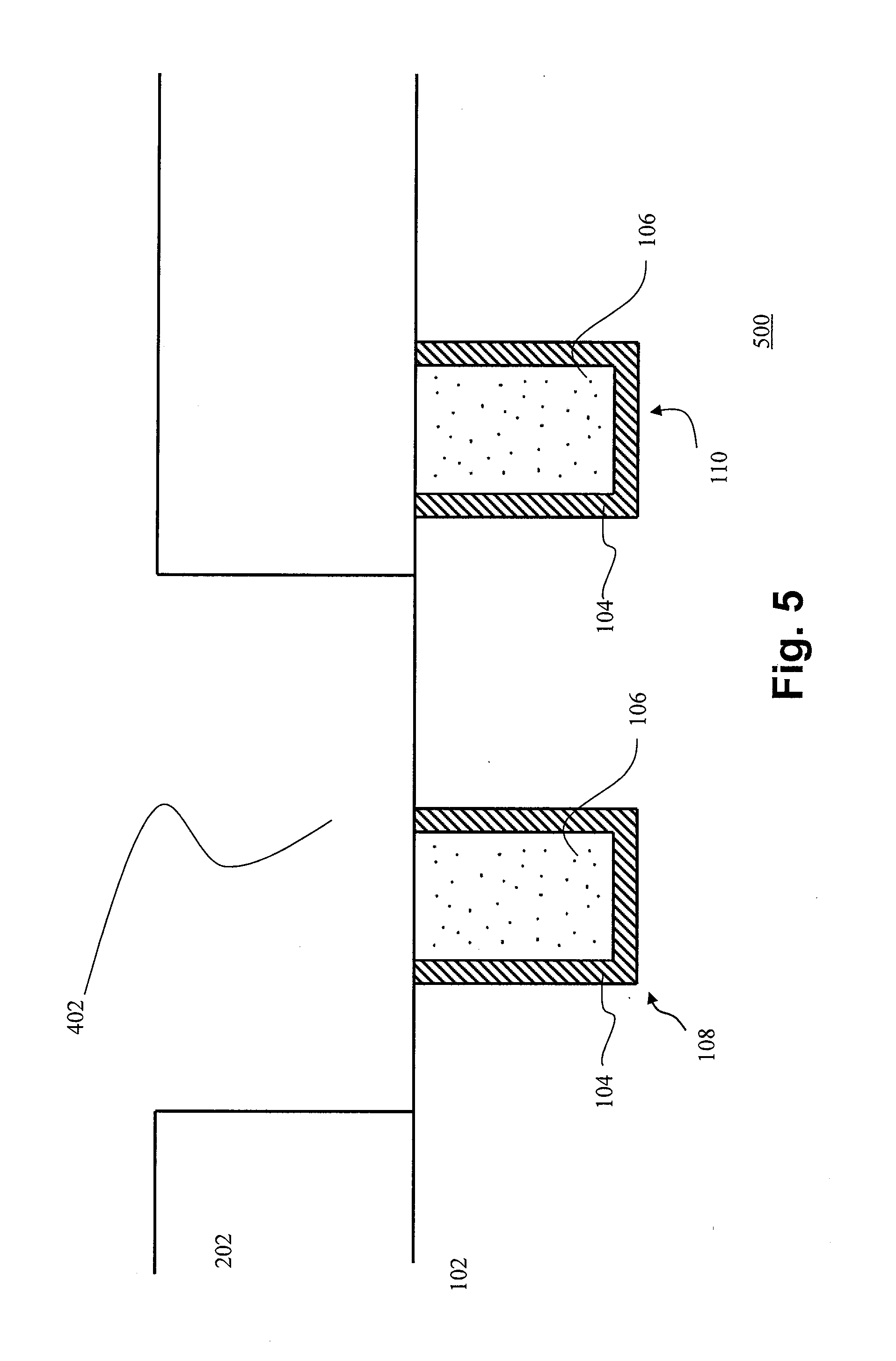
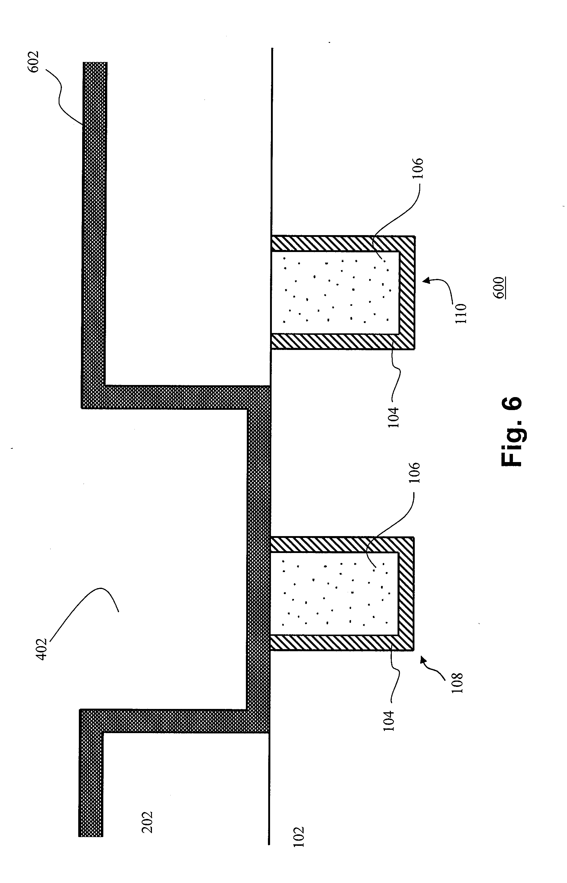
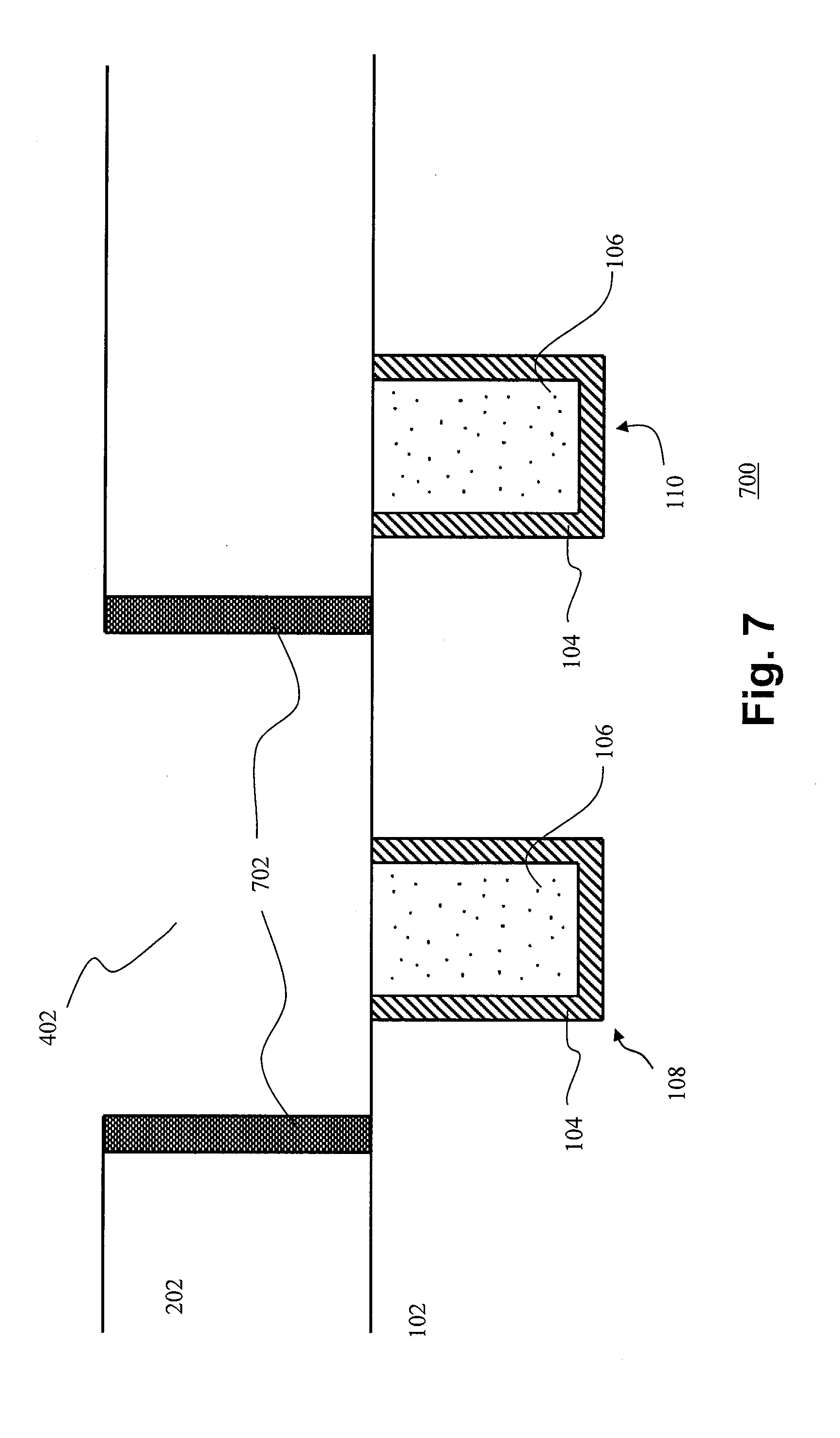
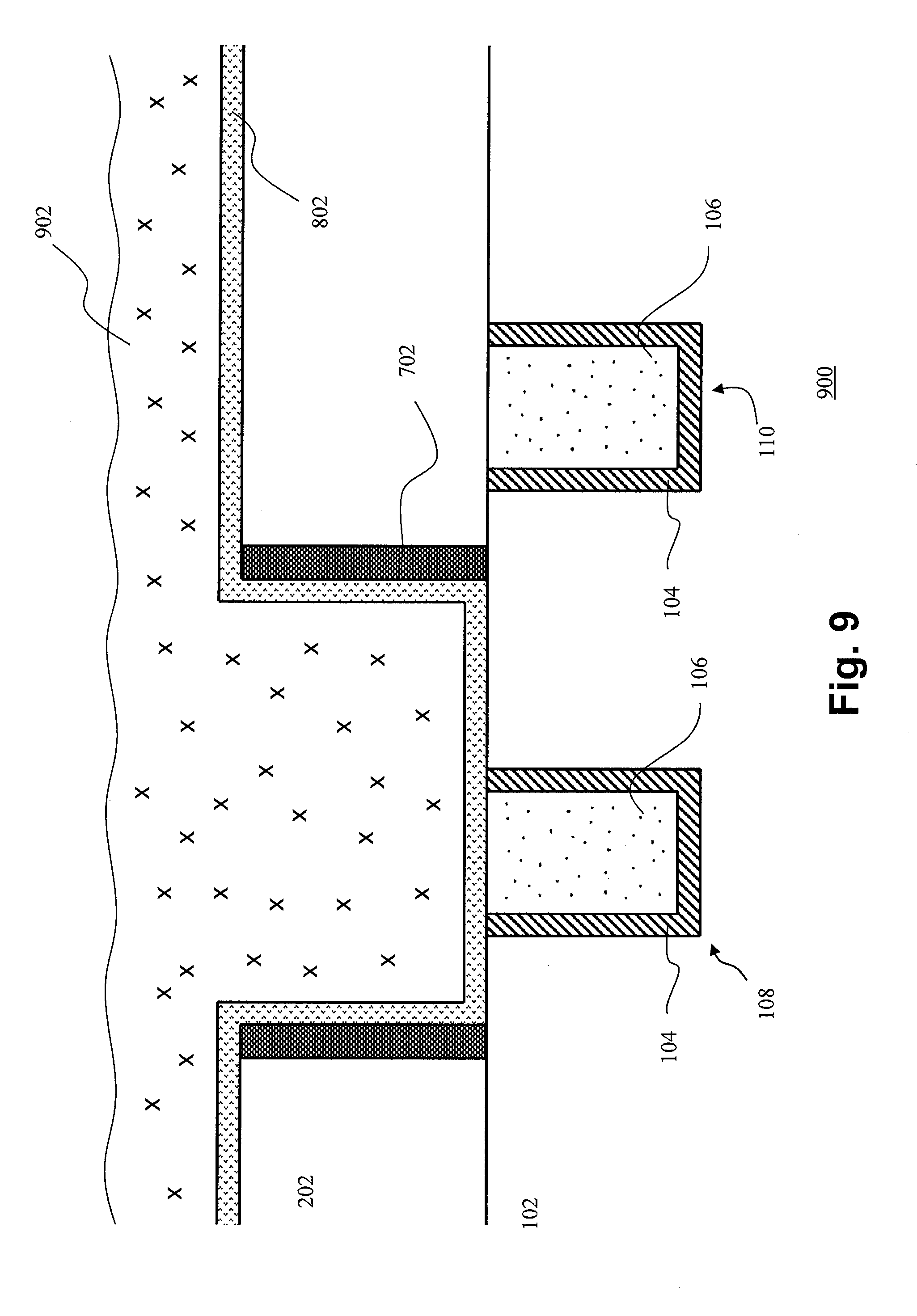
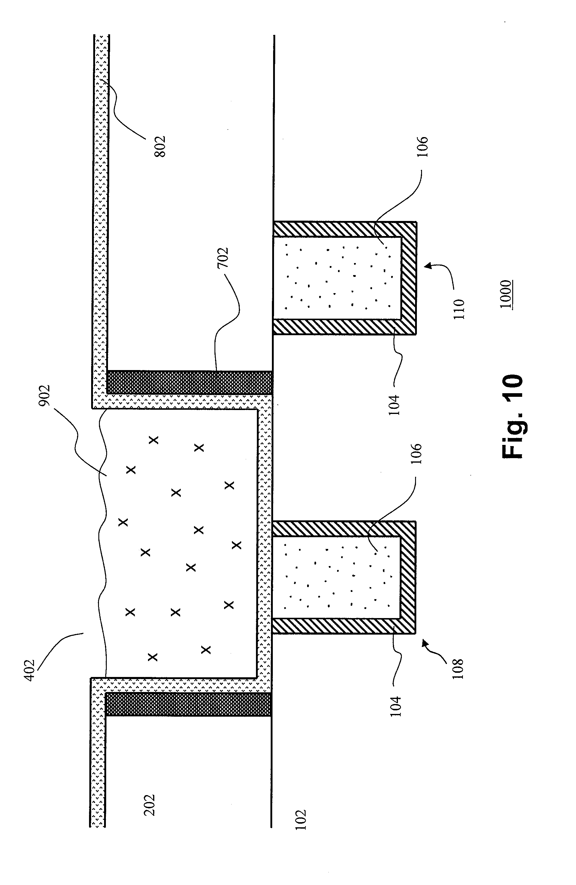
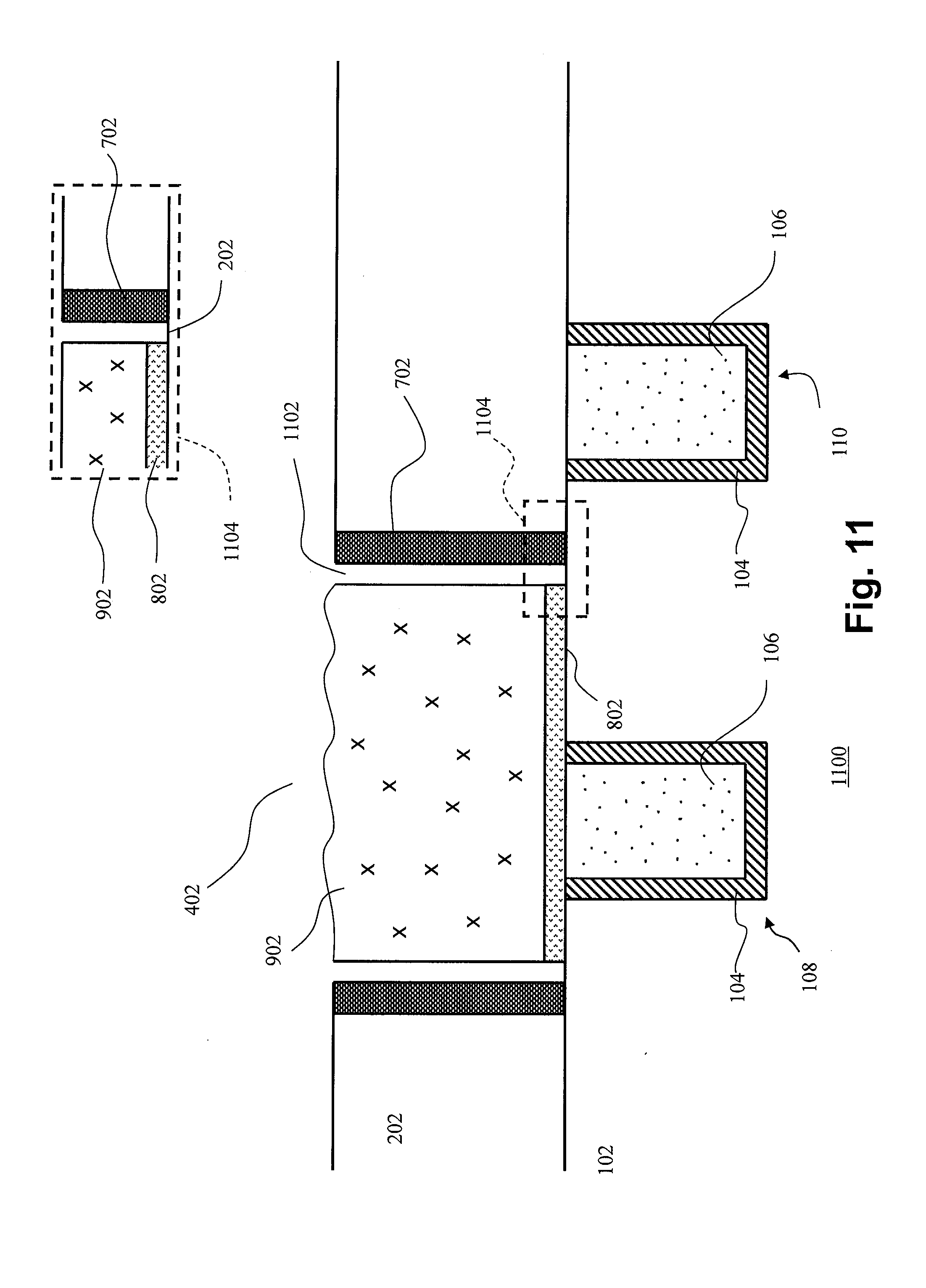
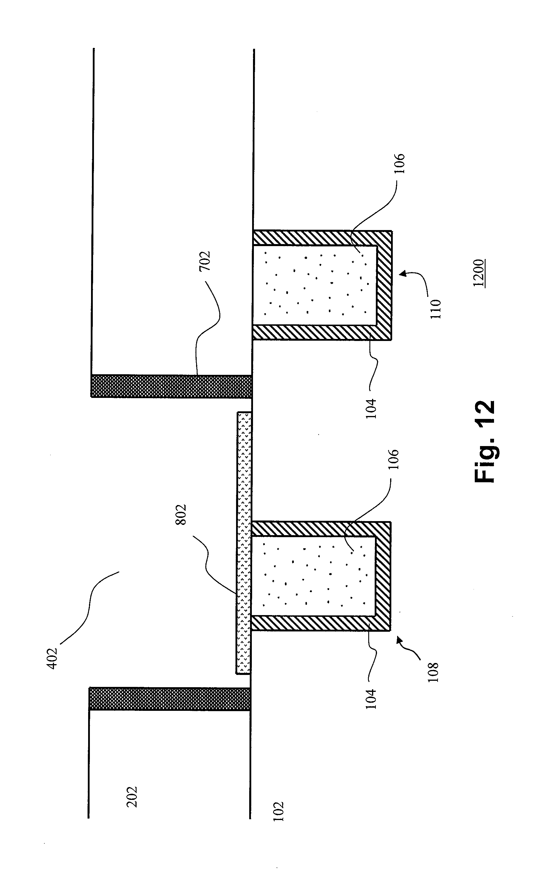
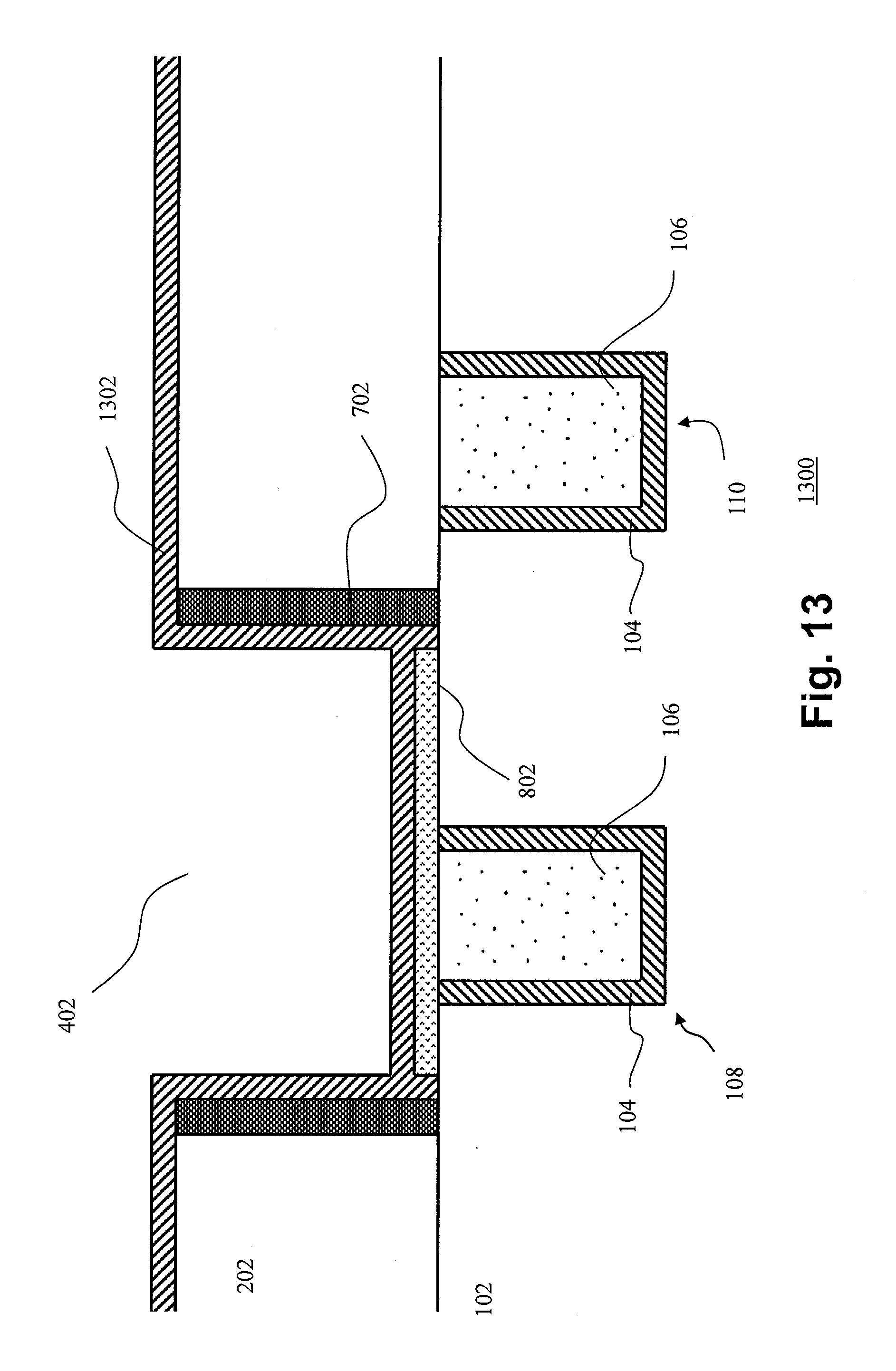
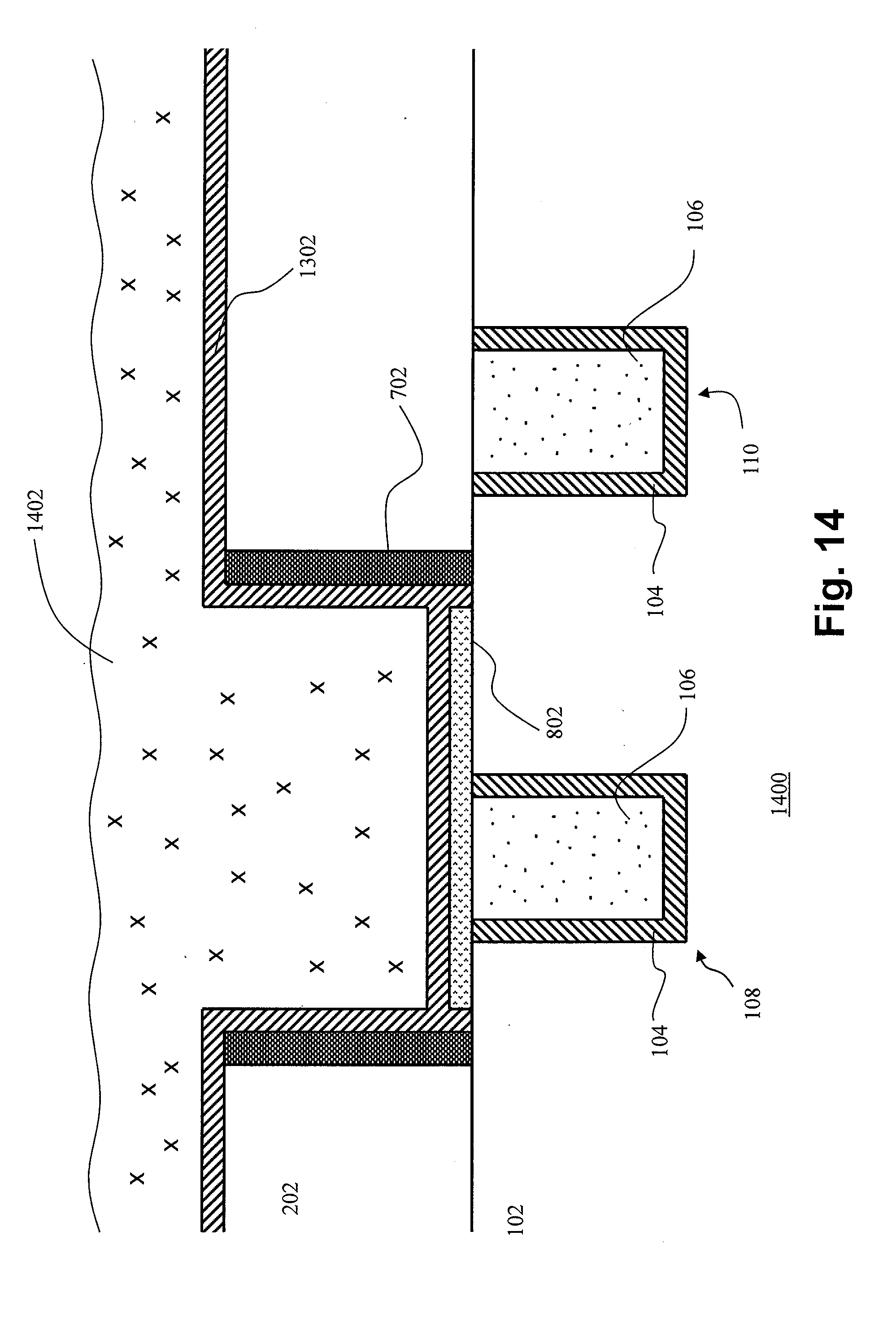
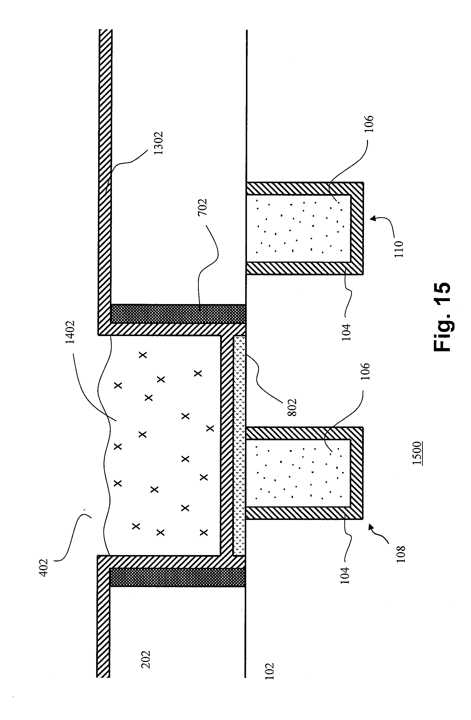
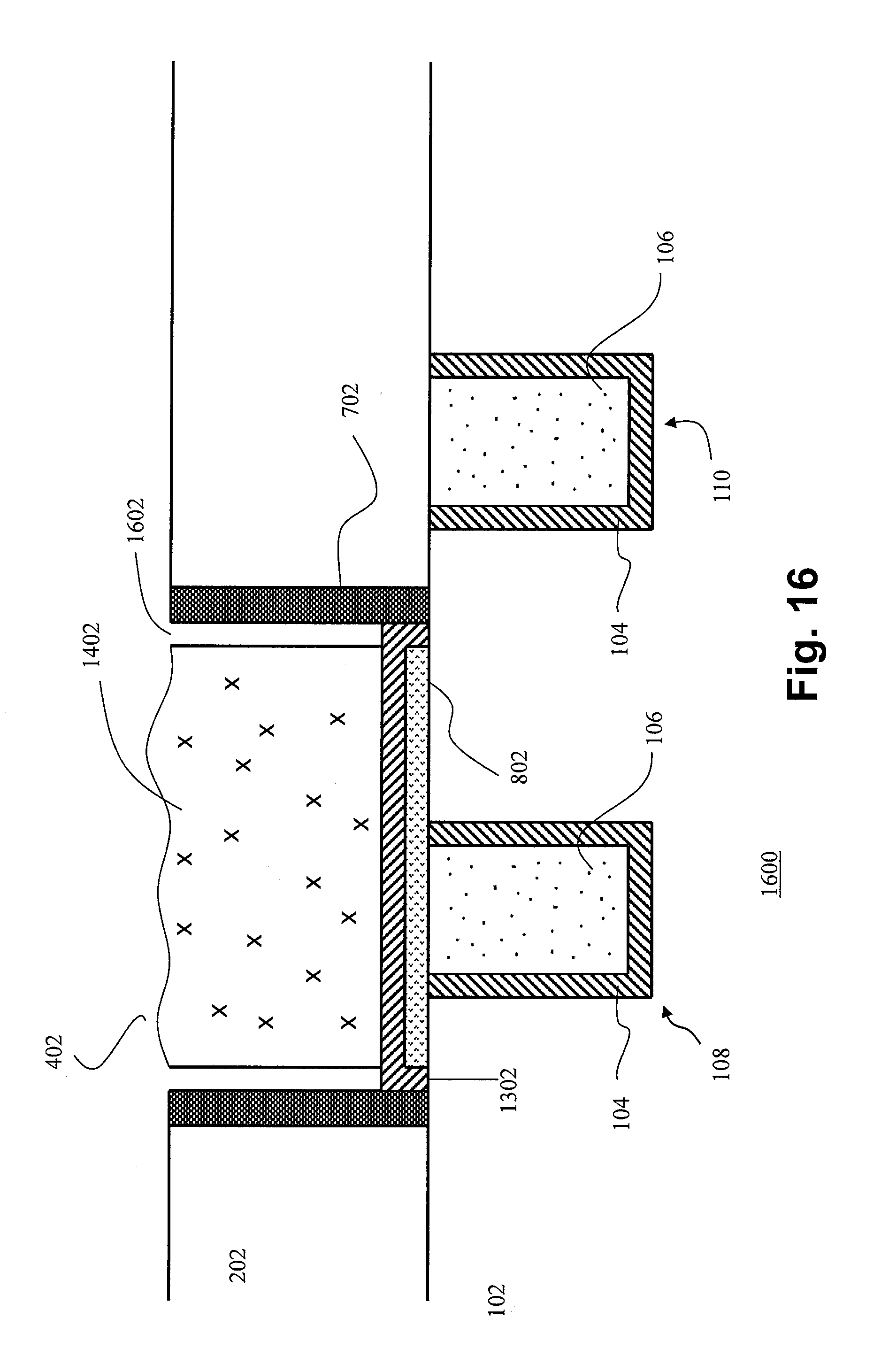
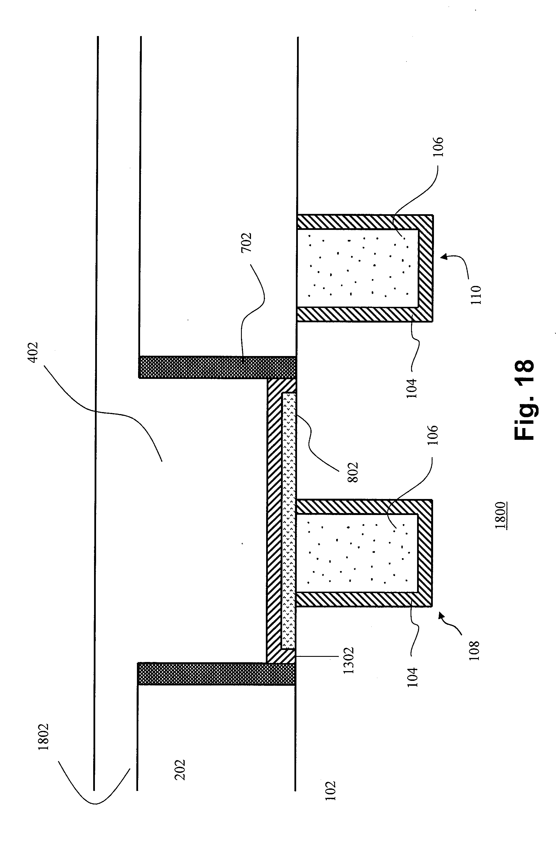
DESCRIPTION OF A REPRESENTATIVE EMBODIMENT