METHOD FOR FABRICATING OXIDES/SEMICONDUCTOR INTERFACES
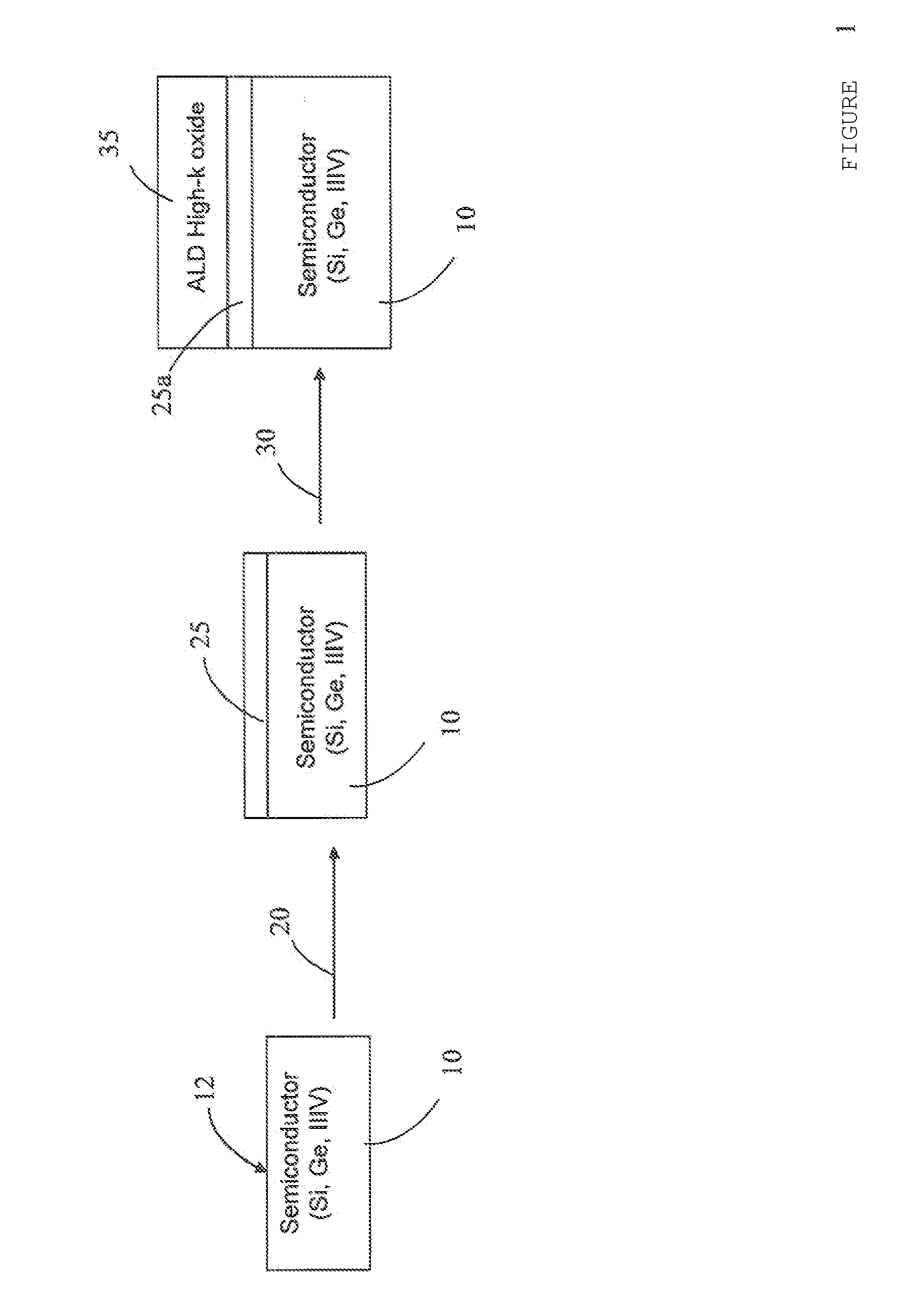
The disclosed subject matter generally relates to semiconductor integrated circuit fabrication technology for metal oxide semiconductor transistors. With the advancement of the semiconductor integrated circuit fabrication technology for metal oxide semiconductor transistors, high dielectric constant (“high-k”) oxide materials are replacing SiO2 in many applications. However, unlike SiO2, high-k oxides are deposited rather than grown by thermal oxidation. With conventional high-k oxide deposition methods such as atomic layer deposition (“ALD”), when a high-k oxide material is deposited on a semiconductor substrate surface, the surface of the semiconductor substrate oxidizes as a result of the oxidizing pulses of the ALD process (O3 or H2O). This results in an undesired low-k oxide interfacial layer between the semiconductor substrate and the deposited high-k oxide layer. This low-k interfacial layer limits equivalent oxide thickness (“EOT”) scaling, increases interface trap density (Dit) for non-Si substrates such as those made from Ge or III/V semiconductors, and can potentially create integration problems, especially for non-Silicon surfaces. This description of the exemplary embodiments is intended to be read in connection with the accompanying drawings, which are to be considered part of the entire written description. In the description, relative terms such as “lower,” “upper,” “horizontal,” “vertical,”, “above,” “below,” “up,” “down,” “top” and “bottom” as well as derivative thereof (e.g., “horizontally,” “downwardly,” “upwardly,” etc.) should be construed to refer to the orientation as then described or as shown in the drawing under discussion. These relative terms are for convenience of description and do not require that the apparatus be constructed or operated in a particular orientation. Terms concerning attachments, coupling and the like, such as “connected” and “interconnected,” refer to a relationship wherein structures are secured or attached to one another either directly or indirectly through intervening structures, as well as both movable or rigid attachments or relationships, unless expressly described otherwise. The term “high-k” as used herein refers to a dielectric constant k that is higher than the dielectric constant of silicon dioxide. Referring to The oxidizing metal 25 is one that forms a high-k metal oxide and can be one of aluminum, barium, srontium, scandium, yttrium, lutetium, titanium, zirconium, hafnium, tantalum, molybdenum, lanthanum, cerium, praseodymium, gadolinium, and dysprosium. The dielectric constants for the corresponding oxides for some of these metals are: The example structure shown in The method of the present disclosure eliminates the formation of an undesirable low-k oxide layer between the high-k oxide and the semiconductor. This is particularly beneficial for non silicon-based semiconductors. The method of the present disclosure also results in low Dit and low EOT and thermally stable gate stacks can be achieved The thickness of the oxidizing metal 25 depends on the thickness of the ALD high-k oxide material layer 35 which will be deposited on top. During an ALD oxide deposition, the duration of the O3 or H2O pulses can be adjusted in order to acquire the deposition process that deposits the desired thickness of the high-k oxide material layer 35 while oxidizing the oxidizing metal layer 25. This pulse duration is directly linked to the thickness of the undesirable low-k interfacial layer that grows during the ALD high-k deposition. Also the total thickness of the ALD high-k oxide material 35 is linked to the thickness of the low-k interfacial layer since thicker ALD high-k oxide means that the semiconductor surface will be exposed to more oxidizing pulses. However, the duration of the oxidizing pulse and the total high-k thickness is not proportional to the thickness of the low-k interfacial layer since as the high-k oxide becomes thicker than the semiconductor surface will be affected less and less. The oxidizing metal 25 should have a thickness approximately equal to the low-k interfacial layer thickness that would grow during a certain ALD high-k oxide deposition process with a specific H2O or O3 pulse duration. A full oxidation of the oxidizing metal 25 is desired but not over oxidation or under oxidation. Over oxidation can lead to creation of low-k interfacial layer at the interface between the underlying semiconductor substrate 10, 110 and the metal oxide 25 Oxidation of the oxidizing metal 25 strongly depends on many different parameters. These parameters are: the selection of the oxidizing metal, the ALD high-k process (thickness, duration of oxidizing pulse), and the thickness of the oxidizing metal. In order to avoid over oxidation or under oxidation, for a particular choice of ALD high-k oxide deposition process and oxidizing metal, several thicknesses of the oxidizing metal would need to be tried and checked to determine the optimal thickness for the oxidizing metal. A rule of thumb could be that the thickness of the oxidizing metal is approximately equal to the thickness of the low-k interfacial layer that the ALD high-k oxide deposition process would create on the semiconductor substrate surface in the absence of the oxidizing metal 25. Although the subject matter has been described in terms of exemplary embodiments, it is not limited thereto. Rather, the appended claims should be construed broadly, to include other variants and embodiments, which may be made by those skilled in the art. By depositing a layer of oxidizing metal on the semiconductor surface first and then depositing a layer of the high-k oxide material over the layer of oxidizing metal by an atomic layer deposition, a high-k metal oxide is formed at the interface between the semiconductor substrate and the high-k oxide and prevents formation of the undesirable low-k semiconductor oxide layer at the semiconductor/high-k oxide interface. 1. A method of fabricating oxide/semiconductor interface comprising:
providing a semiconductor substrate having a surface; depositing a layer of oxidizing metal on the semiconductor surface; and depositing a layer of high-k oxide material over the layer of oxidizing metal by an atomic layer deposition process, whereby the oxidizing metal oxidizes from exposure to the atomic layer deposition process' oxidizing agents O3 and H2O, thus forming a high-k metal oxide layer and prevents formation of undesirable low-k oxide interfacial layer. 2. The method of 3. The method of 4. The method of 5. The method of 6. The method of 7. The method of 8. A method of fabricating oxide/semiconductor interface comprising:
providing a non-planar semiconductor substrate structure having a surface; depositing a layer of oxidizing metal on the non-planar semiconductor substrate surface; and depositing a layer of high-k oxide material over the layer of oxidizing metal by an atomic layer deposition process, whereby the oxidizing metal oxidizes from exposure to the atomic layer deposition process' oxidizing agents O3 and H2O, thus forming a high-k metal oxide layer and prevents formation of undesirable low-k oxide interfacial layer. 9. The method of 10. The method of 11. The method of 12. The method of 13. A method of fabricating oxide/semiconductor interface comprising:
providing a planar semiconductor substrate structure having a surface; depositing a layer of oxidizing metal on the planar semiconductor substrate surface; and depositing a layer of high-k oxide material over the layer of oxidizing metal by an atomic layer deposition process, whereby the oxidizing metal oxidizes from exposure to the atomic layer deposition process' oxidizing agents O3 and H2O, thus forming a high-k metal oxide layer and prevents formation of undesirable low-k oxide interfacial layer. 14. The method of 15. The method of 16. The method of FIELD
BACKGROUND
BRIEF DESCRIPTION OF THE DRAWINGS
DETAILED DESCRIPTION
Al2O3 9 Ta2O5 22 TiO2 80 ZrO2 25 HfO2 25 La2O3 30 Y2O3 15