Semiconductor Device, Method for Manufacturing the Same, and Etchant Used for the Same
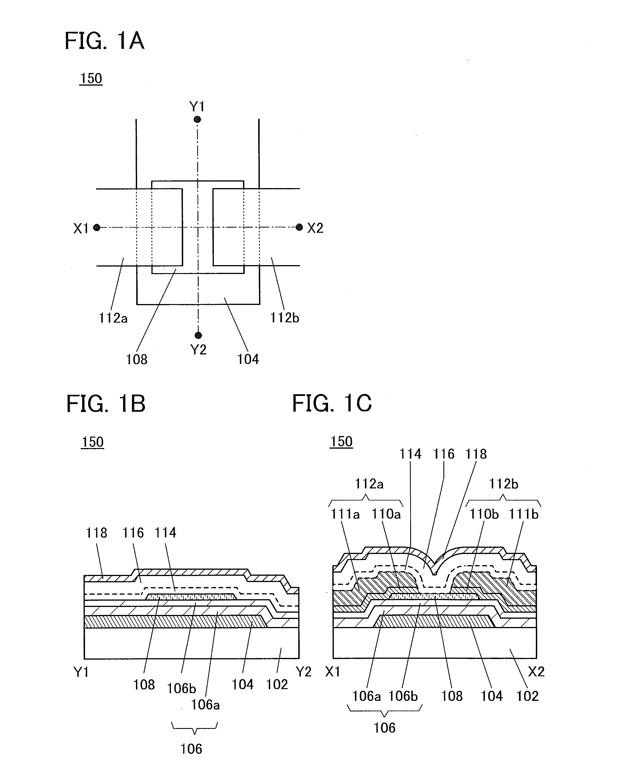
1. Field of the Invention The present invention relates to an object, a method, or a manufacturing method. Further, the present invention relates to a process, a machine, manufacture, or a composition of matter. One embodiment of the present invention relates to a semiconductor device, a display device, a light-emitting device, an electronic device, a manufacturing method thereof, or a driving method thereof. Specifically, one embodiment of the present invention relates to, for example, a semiconductor device using an oxide semiconductor and a method for manufacturing the same. Furthermore, one embodiment of the present invention relates to, for example, an etchant which can be used for a semiconductor device using an oxide semiconductor. Note that in this specification, a semiconductor device refers to a semiconductor element itself or a device including a semiconductor element. As an example of such a semiconductor element, for example, a transistor (a thin film transistor and the like) can be given. In addition, a display device such as a liquid crystal display device includes a semiconductor device in some cases. 2. Description of the Related Art There is a trend in a display device using a transistor (e.g., a liquid crystal panel and an organic EL panel) toward a larger screen. As the screen size becomes larger, in the case of a display device using an active element such as a transistor, a voltage applied to an element varies depending on the position of a wiring which is connected to the element due to wiring resistance, which cause a problem of deterioration of display quality such as display unevenness and a defect in grayscale. Conventionally, an aluminum film has been widely used as a material used for the wiring, the signal line, or the like; moreover, research and development of using a copper film as a material is extensively conducted to further reduce resistance. However, the copper film has poor adhesion to a base film. In addition, diffusion of a copper element in the copper film into a semiconductor layer of a transistor causes degradation in characteristics of the transistor. Note that a silicon-based semiconductor material is widely known as a material for a semiconductor thin film applicable to a transistor, and as another material, an oxide semiconductor has attracted attention (see Patent Document 1). Furthermore, as a method for manufacturing an array substrate for a TFT-LCD, an etchant containing at least one selected from neutral salt, inorganic acid, and organic acid in addition to hydrogen peroxide which can collectively etch a double metal layer including copper is disclosed (see Patent Document 2). According to the structure disclosed in Patent Document 2, a double metal layer including molybdenum (Mo) and copper (Cu) is formed over an amorphous silicon layer; then one from neutral salt, inorganic acid, and organic acid is selected; and by using an etchant in which the selected one, hydrogen peroxide, and hydrogen peroxide stabilizer are mixed, the double metal layer is etched collectively to form a source electrode and a drain electrode. However, the above structure can be only applied to a transistor using an amorphous silicon, that is, a silicon-based semiconductor material as a semiconductor layer; thus, there has been a problem in that the above structure does not have a manufacturing method or an etchant suitable for using a transistor including an oxide semiconductor. In view of the above problems, an object of one embodiment of the present invention is to provide a novel semiconductor device in which a transistor using an oxide semiconductor film includes a wiring, a signal line, or the like formed using a copper-containing metal film. Another object of one embodiment of the present invention is to provide a method for manufacturing a semiconductor device in which a transistor using an oxide semiconductor film includes a wiring, a signal line, or the like formed using a copper-containing metal film. Another object of one embodiment of the present invention is to provide a novel semiconductor device in which a transistor using an oxide semiconductor film includes a copper-containing metal film with a favorable shape. Another object of one embodiment of the present invention is to provide a novel semiconductor device of which productivity is improved. Another object of one embodiment of the present invention is to provide an etchant which can be used for a transistor using an oxide semiconductor film. Another object of one embodiment of the present invention is to provide a novel semiconductor device and a method for manufacturing the novel semiconductor device. Note that the descriptions of these objects do not disturb the existence of other objects. In one embodiment of the present invention, there is no need to achieve all the objects. Objects other than the above objects will be apparent from and can be derived from the description of the specification, the drawings, the claims, and the like. One embodiment of the present invention is a method for manufacturing a semiconductor device including the steps of forming a first conductive film over a substrate; forming an insulating film over the first conductive film; forming an oxide semiconductor film over the insulating film to overlap with the first conductive film; forming a second conductive film including a metal film containing molybdenum as its main component and a metal film containing copper as its main component over the oxide semiconductor film; and etching the second conductive film by an etchant. In the etching step of the second conductive film by the etchant, the oxide semiconductor film is used as an etching stopper film. Another embodiment of the present invention is a method for manufacturing a semiconductor device including the steps of forming a first conductive film over a substrate; forming an insulating film over the first conductive film; forming an oxide semiconductor film and a metal oxide film over the insulating film to overlap with the first conductive film; forming a second conductive film including a metal film containing molybdenum as its main component and a metal film containing copper as its main component over the metal oxide film; and etching the second conductive film by an etchant. In the etching step of the second conductive film by the etchant, the metal oxide film is used as an etching stopper film. In each of the above structures, the oxide semiconductor film is preferably formed using an In-M-Zn oxide (M is Ti, Ga, Y, Zr, Sn, La, Ce, Nd, or Hf). Further, in each of the above structures, the metal oxide film is preferably formed using an In-M oxide (M is Ti, Ga, Y, Zr, Sn, La, Ce, Nd, or Hf). Another embodiment of the present invention is an etchant including an aqueous solution of organic acid and aqueous hydrogen peroxide. The etchant has a function of etching a metal film containing molybdenum as its main component and a metal film containing copper as its main component. The pH of the etchant is greater than or equal to 3 and less than or equal to 6. In the above structure, provided that the ratio of components of the etchant is aqueous hydrogen peroxide:aqueous solution of organic acid=x:y [wt %], y/(x+y) is preferably greater than or equal to 0.7 and less than or equal to 0.9. A semiconductor device, a display device, and an electronic device manufactured by a manufacturing method of the semiconductor device having any of the above structures are also included in one embodiment of the present invention. According to one embodiment of the present invention, a novel semiconductor device in which a transistor using an oxide semiconductor film includes a wiring, a signal line, or the like formed using a copper-containing metal film can be provided. According to another embodiment of the present invention, a method for manufacturing a semiconductor device in which a transistor using an oxide semiconductor film includes a wiring, a signal line, or the like formed using a copper-containing metal film can be provided. According to another embodiment of the present invention, a novel semiconductor device in which a transistor using an oxide semiconductor film includes a copper-containing metal with a favorable shape can be provided. According to another embodiment of the present invention, a novel semiconductor device of which productivity is improved can be provided. According to another embodiment of the present invention, an etchant which can be used for a transistor using an oxide semiconductor film can be provided. According to another embodiment of the present invention, a novel semiconductor device and a method for manufacturing the novel semiconductor device can be provided. Note that the description of these effects does not disturb the existence of other effects. One embodiment of the present invention does not necessarily achieve all the objects listed above. Other effects will be apparent from and can be derived from the description of the specification, the drawings, the claims, and the like. Hereinafter, embodiments will be described with reference to drawings. However, the embodiments can be implemented with various modes. It will be readily appreciated by those skilled in the art that modes and details can be changed in various ways without departing from the spirit and scope of the present invention. Thus, the present invention should not be interpreted as being limited to the following description of the embodiments. In the drawings, the size, the layer thickness, or the region is exaggerated for clarity in some cases. Therefore, embodiments of the present invention are not limited to such a scale. Note that the drawings are schematic views showing ideal examples, and embodiments of the present invention are not limited to shapes or values shown in the drawings. Note that in this specification, ordinal numbers such as “first”, “second”, and “third” are used in order to avoid confusion among components, and the terms do not limit the components numerically. Note that in this specification, terms for describing arrangement, such as “over” “above”, “under”, and “below”, are used for convenience in describing a positional relation between components with reference to drawings. Furthermore, the positional relation between components is changed as appropriate in accordance with a direction in which each component is described. Thus, there is no limitation on terms used in this specification, and description can be made appropriately depending on the situation. In this specification and the like, a transistor is an element having at least three terminals of a gate, a drain, and a source. In addition, the transistor has a channel region between a drain (a drain terminal, a drain region, or a drain electrode layer) and a source (a source terminal, a source region, or a source electrode layer), and current can flow through the drain, the channel region, and the source. Note that in this specification and the like, a channel region refers to a region through which current mainly flows. Further, functions of a source and a drain might be switched when transistors having different polarities are employed or a direction of current flow is changed in circuit operation, for example. Therefore, the terms “source” and “drain” can be switched in this specification and the like. Note that in this specification and the like, the expression “electrically connected” includes the case where components are connected through an “object having any electric function”. There is no particular limitation on an “object having any electric function” as long as electric signals can be transmitted and received between components that are connected through the object. Examples of an “object having any electric function” are a switching element such as a transistor, a resistor, an inductor, a capacitor, and elements with a variety of functions as well as an electrode and a wiring. In this embodiment, a semiconductor device of one embodiment of the present invention and a method for manufacturing the semiconductor device will be described with reference to The semiconductor device 150 illustrated in In Further, the conductive film 112 By employing a two-layer structure including the metal film containing molybdenum as its main component and the metal film containing copper as its main component as described above for the conductive films 112 The metal film containing molybdenum as its main component is formed over the oxide semiconductor film 108 as the conductive films 110 Furthermore, the metal film containing copper as its main component is formed as the conductive films 111 Note that as one of the characteristics required for the formation of the conductive films 112 Here, a method for manufacturing the conductive films 112 In one embodiment of the present invention, an etchant including aqueous solution of organic acid and aqueous hydrogen peroxide is used in the formation of the conductive films 112 The etchant is used at the formation of the conductive films 112 In order to manufacture the conductive films 112 When the etchant is applied, the metal film containing copper as its main component used as the upper layer film of the conductive films 112 However, in one embodiment of the present invention, the etchant including an aqueous solution of organic acid and aqueous hydrogen peroxide is used, and the pH of the etchant is greater than or equal to 3 and less than or equal to 6. Furthermore, provided that the ratio of components of the etchant is aqueous hydrogen peroxide:aqueous solution of organic acid=x:y [wt %], y/(x+y) is greater than or equal to 0.7 and less than or equal to 0.9, preferably greater than or equal to 0.8 and less than or equal to 0.85. With such an etchant, the phenomenon (undercut) in which the metal film containing molybdenum as its main component is positioned on the inner side than the metal film containing copper as its main component can be suppressed, and the metal film containing copper as its main component and the metal film containing molybdenum as its main component can be etched collectively. Thus, a semiconductor device with a favorable cross-sectional shape can be obtained. The base film of the conductive films 112 In this manner, in the semiconductor device of one embodiment of the present invention and the method for manufacturing the semiconductor device, at the formation of the conductive films 112 Next, details of other elements included in the semiconductor device illustrated in There is no particular limitation on the property of a material and the like of the substrate 102 as long as the material has heat resistance enough to withstand at least heat treatment to be performed later. For example, a glass substrate, a ceramic substrate, a quartz substrate, a sapphire substrate, or the like may be used as the substrate 102. Alternatively, a single crystal semiconductor substrate or a polycrystalline semiconductor substrate made of silicon, silicon carbide, or the like, a compound semiconductor substrate made of silicon germanium or the like, an SOI substrate, or the like may be used as the substrate 102. Furthermore, any of these substrates further provided with a semiconductor element may be used as the substrate 102. In the case where a glass substrate is used as the substrate 102, a glass substrate having any of the following sizes can be used: the 6th generation (1500 mm×1850 mm), the 7th generation (1870 mm×2200 mm), the 8th generation (2200 mm×2400 mm), the 9th generation (2400 mm×2800 mm), and the 10th generation (2950 mm×3400 mm) Thus, a large-sized display device can be manufactured. Still further alternatively, a flexible substrate may be used as the substrate 102, and the semiconductor device 150 and the like may be provided directly on the flexible substrate. Note that in this specification and the like, a transistor can be formed using a variety of substrates. The type of a substrate is not limited to a certain type. As the substrate, a semiconductor substrate (e.g., a single crystal substrate or a silicon substrate), an SOI substrate, a glass substrate, a quartz substrate, a plastic substrate, a metal substrate, a stainless steel substrate, a substrate including stainless steel foil, a tungsten substrate, a substrate including tungsten foil, a flexible substrate, an attachment film, paper including a fibrous material, a base material film, or the like can be used, for example. As an example of a glass substrate, a barium borosilicate glass substrate, an aluminoborosilicate glass substrate, a soda lime glass substrate, or the like can be given. Examples of a flexible substrate include a flexible synthetic resin such as plastics typified by polyethylene terephthalate (PET), polyethylene naphthalate (PEN), and polyether sulfone (PES), and acrylic. For an attachment film, polypropylene, polyester, polyvinyl fluoride, polyvinyl chloride, or the like can be used, for example. Examples of the material for the base film include polyester, polyamide, polyimide, inorganic vapor deposition film, and paper. Specifically, the use of semiconductor substrates, single crystal substrates, SOI substrates, or the like enables the manufacture of small-sized transistors with a small variation in characteristics, size, shape, or the like and with high current capability. A circuit using such transistors achieves lower power consumption of the circuit or higher integration of the circuit. Note that a transistor may be formed using one substrate, and then the transistor may be transferred to another substrate. In addition to the above substrates over which the transistor can be formed, a paper substrate, a cellophane substrate, a stone substrate, a wood substrate, a cloth substrate (including a natural fiber (e.g., silk, cotton, or hemp), a synthetic fiber (e.g., nylon, polyurethane, or polyester), a regenerated fiber (e.g., acetate, cupra, rayon, or regenerated polyester), or the like), a leather substrate, a rubber substrate, or the like can be used as a substrate to which the transistor is transferred. When such a substrate is used, a transistor with excellent properties or a transistor with low power consumption can be formed, a device with high durability, high heat resistance can be provided, or reduction in weight or thickness can be achieved. The oxide semiconductor film 108 is formed using an In-M-Zn oxide W is Ti, Ga, Y, Zr, Sn, La, Ce, Nd, or Hf). For the oxide semiconductor film 108, for example, In—Ga—Zn based oxide can be used. Note that here, for example, an “In—Ga—Zn-based oxide” means an oxide containing In, Ga, and Zn as its main components and there is no limitation on the ratio of In:Ga:Zn. The In—Ga—Zn-based oxide may contain another metal element in addition to In, Ga, and Zn. As the insulating films 106 Note that the insulating film 106 Using hafnium oxide for the insulating films 106 In this embodiment, a silicon nitride film is formed as the insulating film 106 For the conductive films 112 As each of the insulating films 114, 116 and 118 serving as a protective insulating film of the semiconductor device 150, an insulating film including at least one of the following films formed by a plasma CVD method, a sputtering method, or the like can be used: a silicon oxide film, a silicon oxynitride film, a silicon nitride oxide film, a silicon nitride film, an aluminum oxide film, a hafnium oxide film, an yttrium oxide film, a zirconium oxide film, a gallium oxide film, a tantalum oxide film, a magnesium oxide film, a lanthanum oxide film, a cerium oxide film, and a neodymium oxide film. An insulating film 114 in contact with the oxide semiconductor film 108 serving as a channel region of the semiconductor device 150 is preferably an oxide insulating film, and an insulating film capable of releasing oxygen is used. In other words, the insulating film capable of releasing oxygen is an insulating film including a region (oxygen-excess region) containing oxygen in excess of that in the stoichiometric composition. In order to provide the oxygen-excess region in the insulating film 114, the insulating film 114 is formed in an oxygen atmosphere, for example. Alternatively, oxygen may be introduced into the deposited insulating film 114 to provide the oxygen-excess region therein. As a method for introducing oxygen, an ion implantation method, an ion doping method, a plasma immersion ion implantation method, plasma treatment, or the like may be employed. The use of the insulating film capable of releasing oxygen as the insulating film 114 can reduce the number of oxygen vacancies in the oxide semiconductor film 108 by transferring oxygen to the oxide semiconductor film 108 serving as a channel region of the semiconductor device 150. For example, the number of oxygen vacancies in the oxide semiconductor film 108 can be reduced by using an insulating film having the following feature: the number of oxygen molecules released from the insulating film by heat treatment at a temperature higher than or equal to 100° C. and lower or equal to 700° C., preferably higher than or equal to 100° C. and lower than or equal to 500° C. is greater than or equal to 1.0×10¹⁸molecules/cm3when measured by thermal desorption spectroscopy (hereinafter referred to as TDS). The thickness of the insulating film 114 can be greater than or equal to 5 nm and less than or equal to 150 nm, preferably greater than or equal to 5 nm and less than or equal to 50 nm, more preferably greater than or equal to 10 nm and less than or equal to 30 nm. The thickness of the insulating film 116 can be greater than or equal to 30 nm and less than or equal to 500 nm, preferably greater than or equal to 150 nm and less than or equal to 400 nm. Furthermore, the insulating films 114 and 116 can be formed using insulating films formed of the same kinds of materials; thus, a boundary between the insulating films 114 and 116 cannot be clearly observed in some cases. Thus, in this embodiment, the boundary between the insulating films 114 and 116 is shown by a dashed line. Although a two-layer structure of the insulating films 114 and 116 is described in this embodiment, the present invention is not limited to this. For example, a single-layer structure of the insulating film 114, a single-layer structure of the insulating film 116, or a stacked-layer structure including three or more layers may be used. Next, an example of a method for manufacturing the semiconductor device illustrated in First, the conductive film 104 serving as a gate electrode layer is formed over the substrate 102. Then, the insulating film 106 serving as a gate insulating film is formed over the substrate 102 and the conductive film 104. Note that the insulating film 106 includes the insulating films 106 Note that the substrate 102, the conductive film 104, and the insulating films 106 By providing the silicon nitride film as the insulating film 106 Next, the oxide semiconductor film 108 is formed over the insulating film 106 to overlap with the conductive film 104 (see The oxide semiconductor film 108 can be formed using any of the materials described above. In this embodiment, as the oxide semiconductor film 108, an In—Ga—Zn oxide film, which is formed using a metal oxide target with In:Ga:Zn=1:1:1, is used. The oxide semiconductor film 108 can be formed in such a manner that an oxide semiconductor film is formed over the insulating film 106, the oxide semiconductor film is patterned so that a desired region thereof remains, and then unnecessary regions are etched. After formation of the oxide semiconductor film 108, heat treatment is preferably performed. The heat treatment is preferably performed at a temperature of higher than or equal to 250° C. and lower than or equal to 650° C., preferably higher than or equal to 300° C. and lower than or equal to 500° C., more preferably higher than or equal to 350° C. and lower than or equal to 450° C., in an inert gas atmosphere, an atmosphere containing an oxidizing gas at 10 ppm or more, or a reduced pressure atmosphere. Alternatively, the heat treatment may be performed first in an inert gas atmosphere, and then another heat treatment is performed in an atmosphere containing an oxidizing gas at 10 ppm or more in order to compensate oxygen released from the oxide semiconductor film 108. By this heat treatment, impurities such as hydrogen and water can be removed from at least one of the insulating film 106 Note that stable electrical characteristics can be effectively imparted to the semiconductor device 150 in which the oxide semiconductor film 108 serves as a channel region by reducing the concentration of impurities in the oxide semiconductor film 108 to make the oxide semiconductor film 108 intrinsic or substantially intrinsic. Next, a stacked-layer film of the conductive film 110 and the conductive film 111 is formed over the insulating film 106 and the oxide semiconductor film 108 (see The conductive film 110 can be formed using any of the materials described above as the materials of the conductive films 110 Next, a resist is applied over the conductive film 111 and is patterned, whereby resist masks 140 The resist masks 140 Next, an etchant 180 is applied from above the resist masks 140 The etchant 180 used for etching the conductive films 110 and 111 is an etchant including an aqueous solution of an organic acid and hydrogen peroxide, and the pH of the etchant 180 is greater than or equal to 3 and less than or equal to 6. Furthermore, provided that the ratio of components of the etchant 180 is aqueous hydrogen peroxide:aqueous solution of organic acid=x:y [wt %], y/(x+y) is greater than or equal to 0.7 and less than or equal to 0.9, preferably greater than or equal to 0.8 and less than or equal to 0.85. With the etchant 180 including such components, a phenomenon in which the molybdenum film is positioned on an inner side than the copper film can be suppressed, whereby a favorable cross-sectional shape can be obtained. At the time of etching the conductive films 110 and 111, the oxide semiconductor film 108 is used as an etching stopper. When the etchant 180 has the components described above, the etching rate of the oxide semiconductor film 108 can be lower than those of the conductive films 112 Next, the resist masks 140 The resist masks 140 Next, the insulating films 114, 116, and 118 serving as a protective insulating film are formed over the oxide semiconductor film 108, the conductive film 112 The insulating films 114, 116 and 118 can be formed using any of the materials described above. In this embodiment, a silicon oxynitride film capable of releasing oxygen is used as the insulating films 114 and 116, and a silicon nitride film is used as the insulating film 118. By using a silicon nitride film, impurities and the like that enter the oxide semiconductor film 108 from the outside can be reduced. Through the above manufacturing steps, the semiconductor device 150 illustrated in The structures, the methods, and the like described in this embodiment can be combined as appropriate with any of the structures, the methods, and the like described in the other embodiments. In this embodiment, a semiconductor device and a manufacturing method of the semiconductor device which are different from those in Embodiment 1 are described using The semiconductor device 160 illustrated in The semiconductor device 160 also includes an opening portion 142 Note that the insulating film 106 serves as a first gate insulating film of the semiconductor device 160, and the insulating films 114, 116, and 118 serve as a second gate insulating film of the semiconductor device 160. Furthermore, the conductive film 120 In the channel width direction (a direction indicated by a dashed-dotted line Y3-Y4 in In the channel width direction (a direction indicated by a dashed-dotted line Y3-Y4 in The semiconductor device 160 has a structure in which the conductive film 104 serving as a gate electrode layer and the conductive film 120 With the structure described above, carriers flow in a wide region of the oxide semiconductor film 108 without being limited to the interface between the insulating film 106 (specifically, the insulating film 106 As a result, the on-state current of the semiconductor device 160 is increased, and the field-effect mobility is increased to greater than or equal to 10 cm2/V·s or to greater than or equal to 20 cm2/V·s, for example. Note that here, the field-effect mobility is not an approximate value of the mobility as the physical property of the oxide semiconductor film but is an index of current drive capability and the apparent field-effect mobility of a saturation region of the transistor. Note that an increase in field-effect mobility becomes significant when the channel length (also referred to as L length) of the transistor is greater than or equal to 0.5 μm and less than or equal to 6.5 μm, preferably greater than 1 μm and less than 6 μm, further preferably greater than 1 μm and less than or equal to 4 μm, still further preferably greater than 1 μm and less than or equal to 3.5 μm, yet still further preferably greater than 1 μm and less than or equal to 2.5 μm. With a short channel length more than or equal to 0.5 μm and less than or equal to 6.5 μm, the channel width can also be short. Defects are formed at end portions of the oxide semiconductor film 108, which is processed by etching or the like, because of damage due to the processing, and the end portions are polluted by attachment of impurities or the like. For this reason, in the case where only one of the conductive film 104 serving as a gate electrode layer and the conductive film 120 In the case where the n-type regions are provided between the conductive film 112 Further, an electric field from the outside can be blocked by the conductive film 104 serving as a gate electrode layer and the conductive film 120 The BT stress test is one kind of accelerated test and can evaluate, in a short time, change in characteristics (i.e., a change over time) of transistors, which is caused by long-term use. In particular, the amount of change in threshold voltage of the transistor between before and after the BT stress test is an important indicator when examining the reliability of the transistor. If the amount of change in the threshold voltage between before and after the BT stress test is small, the transistor has higher reliability. Next, a method for manufacturing the semiconductor device 160 is described with reference to First, follow the steps up to the step illustrated in The opening portions 142 The opening portions 142 Next, a conductive film 120 is formed over the insulating film 118 so as to cover the opening portions 142 For the conductive film 120, for example, a material including one of indium (In), zinc (Zn), and tin (Sn) can be used. In particular, for the conductive film 120, a light-transmitting conductive material such as indium oxide containing tungsten oxide, indium zinc oxide containing tungsten oxide, indium oxide containing titanium oxide, indium tin oxide containing titanium oxide, indium tin oxide (ITO), indium zinc oxide, or indium tin oxide to which silicon oxide is added can be used. The conductive film 120 can be formed by a sputtering method, for example. Then, the conductive film 120 is processed into a desired shape, whereby the conductive films 120 To form the conductive films 120 Formation steps of components other than the opening portions 142 Through the above steps, a semiconductor device which includes an oxide semiconductor film can have favorable electrical characteristics. Furthermore, the semiconductor device which includes the oxide semiconductor film can have high reliability. The oxide semiconductor film 108 and the conductive films 112 As illustrated in As illustrated in Although not illustrated in As shown in For example, in this specification and the like, a display element, a display device which is a device including a display element, a light-emitting element, and a light-emitting device which is a device including a light-emitting element can employ various modes and can include various elements. Examples of a display element, a display device, a light-emitting element, or a light-emitting device include an EL (electroluminescent) element (e.g., an EL element including organic and inorganic materials, an organic EL element, or an inorganic EL element), an LED (e.g., a white LED, a red LED, a green LED, or a blue LED), a transistor (a transistor which emits light depending on current), an electron emitter, a liquid crystal element, electronic ink, an electrophoretic element, a grating light valve (GLV), a plasma display panel (PDP), a display device using a micro electro mechanical system (MEMS), a digital micromirror device (DMD), a digital micro shutter (DMS), an interferometric modulator display (IMOD), an electrowetting element, a piezoelectric ceramic display, and a carbon nanotube, which are display media whose contrast, luminance, reflectivity, transmittance, or the like is changed by electromagnetic action. Note that examples of display devices having EL elements include an EL display. Examples of display devices including electron emitters are a field emission display (FED) and an SED-type flat panel display (SED: surface-conduction electron-emitter display). Examples of display devices including liquid crystal elements include a liquid crystal display (e.g., a transmissive liquid crystal display, a transflective liquid crystal display, a reflective liquid crystal display, a direct-view liquid crystal display, or a projection liquid crystal display). An example of a display device including electronic ink or electrophoretic elements is electronic paper. An insulating film 188 functioning as a planarization film may be formed over the insulating film 118 as illustrated in In this embodiment, an example in which an oxide semiconductor is included in a channel region of a transistor is described. However, one embodiment of the present invention is not limited thereto. Depending on cases or conditions, regions such as a channel region, source and drain regions, and/or a LDD region may include a semiconductor including silicon, germanium, or the like. In the case of using silicon, amorphous silicon, polysilicon, single crystal silicon, or the like may be included. Note that the structures, methods, and the like described in this embodiment can be used as appropriate in combination with any of the structures, methods, and the like described in the other embodiments. In this embodiment, a semiconductor device and a manufacturing method of the semiconductor device which are different from those in Embodiment Tare described using A semiconductor device in A semiconductor device illustrated in The metal oxide films 108 For the oxide semiconductor film 108, for example, a material described in Embodiment 1, which is formed using an In-M-Zn oxide (M is Ti, Ga, Y, Zr, Sn, La, Ce, Nd, or Hf), is used. For the metal oxide film 108 In the manufacturing step of the conductive films 112 In the step of forming the conductive films 112 Here, For easy understanding, the band structure shows the energy (Ec) at the bottom of the conduction band of each of the insulating film 106 As illustrated in As illustrated in To form a continuous junction between the oxide semiconductor film 108, the metal oxide film 108 With the band structure of By providing the metal oxide film 108 When a voltage is applied to each of the semiconductor devices illustrated in In In such a structure, the oxide semiconductor film 108 serves as a main path of current and functions as a channel region when a voltage is applied to the semiconductor device in In It is preferable that the metal oxide film 108 The thickness of the metal oxide film 108 Note that as shown in When the metal oxide film 108 When an In-M-Zn oxide is used for the metal oxide film 108 Further, in the case where each of the oxide semiconductor film 108 and the metal oxide film 108 Furthermore, in the case where the oxide semiconductor film 108 and the metal oxide film 108 In the case where the oxide semiconductor film 108 is formed of an In-M-Zn oxide (M is Ti, Ga, Y, Zr, Sn, La, Ce, Nd, or Hf) and a target having the atomic ratio of metal elements of In:MZn=x1:y1:z1is used for depositing the oxide semiconductor film 108, x1/y1is preferably greater than or equal to ⅓ and less than or equal to 6, further preferably greater than or equal to 1 and less than or equal to 6, and z1/y1is preferably greater than or equal to ⅓ and less than or equal to 6, further preferably greater than or equal to 1 and less than or equal to 6. Note that when z1/y1is greater than or equal to 1 and less than or equal to 6, a c-axis aligned crystalline oxide semiconductor (CAAC-OS) film to be described later as the oxide semiconductor film 108 is easily formed. Typical examples of the atomic ratio of the metal elements of the target are In:MZn=1:1:1, In:M:Zn=1:1:1.2, In:MZn=3:1:2, In:MZn=4:2:4.1, and the like. In the case where the metal oxide film 108 Further, in the case where the metal oxide film 108 Note that the atomic ratio of each of the oxide semiconductor film 108, the metal oxide film 108 Note that the structures, methods, and the like described in this embodiment can be used as appropriate in combination with any of the structures, methods, and the like described in the other embodiments. An oxide semiconductor film that can be used for the semiconductor device of one embodiment of the present invention and that can be formed in the method for manufacturing the semiconductor device will be described in detail in this embodiment. An oxide semiconductor film is classified roughly into a single-crystal oxide semiconductor film and a non-single-crystal oxide semiconductor film. The non-single-crystal oxide semiconductor film includes any of a c-axis aligned crystalline oxide semiconductor (CAAC-OS) film, a polycrystalline oxide semiconductor film, a microcrystalline oxide semiconductor film, an amorphous oxide semiconductor film, and the like. First, a CAAC-OS film is described. The CAAC-OS film is one of oxide semiconductor films having a plurality of c-axis aligned crystal parts. In a transmission electron microscope (TEM) image of the CAAC-OS film, a boundary between crystal parts, that is, a grain boundary is not clearly observed. Thus, in the CAAC-OS film, a reduction in electron mobility due to the grain boundary is less likely to occur. According to the TEM image of the CAAC-OS film observed in a direction substantially parallel to a sample surface (cross-sectional TEM image), metal atoms are arranged in a layered manner in the crystal parts. Each metal atom layer has a shape reflecting a surface over which the CAAC-OS film is formed (hereinafter, a surface over which the CAAC-OS film is formed is referred to as a formation surface) or a top surface of the CAAC-OS film, and is arranged parallel to the formation surface or the top surface of the CAAC-OS film. On the other hand, according to the TEM image of the CAAC-OS film observed in a direction substantially perpendicular to the sample surface (plan TEM image), metal atoms are arranged in a triangular or hexagonal configuration in the crystal parts. However, there is no regularity of arrangement of metal atoms between different crystal parts. From the results of the cross-sectional TEM image and the plan TEM image, alignment is found in the crystal parts in the CAAC-OS film. In this specification, a term “parallel” indicates that the angle formed between two straight lines is greater than or equal to −10° and less than or equal to 10°, and accordingly also includes the case where the angle is greater than or equal to −5° and less than or equal to 5°. In addition, the term “perpendicular” indicates that the angle formed between two straight lines is greater than or equal to 80° and less than or equal to 100°, and accordingly also includes the case where the angle is greater than or equal to 85° and less than or equal to 95°. Most of the crystal parts included in the CAAC-OS film each fit inside a cube whose one side is less than 100 nm Thus, there is a case where a crystal part included in the CAAC-OS film fits inside a cube whose one side is less than 10 nm, less than 5 nm, or less than 3 nm. Note that when a plurality of crystal parts included in the CAAC-OS film are connected to each other, one large crystal region is formed in some cases. For example, a crystal region with an area of 2500 mm2or more, 5 μm2or more, or 1000 μm2or more is observed in some cases in the plan TEM image. A CAAC-OS film is subjected to structural analysis with an X-ray diffraction (XRD) apparatus. For example, when the CAAC-OS film including an InGaZnO4crystal is analyzed by an out-of-plane method, a peak appears frequently when the diffraction angle (2θ) is around 31°. This peak is derived from the (009) plane of the InGaZnO4crystal, which indicates that crystals in the CAAC-OS film have c-axis alignment, and that the c-axes are aligned in a direction substantially perpendicular to the formation surface or the top surface of the CAAC-OS film. On the other hand, when the CAAC-OS film is analyzed by an in-plane method in which an X-ray enters a sample in a direction substantially perpendicular to the c-axis, a peak appears frequently when 2θ is around 56°. This peak is derived from the (110) plane of the InGaZnO4crystal. Here, analysis (φ scan) is performed under conditions where the sample is rotated around a normal vector of a sample surface as an axis (0 axis) with 2θ fixed at around 56°. In the case where the sample is a single-crystal oxide semiconductor film of InGaZnO4, six peaks appear. The six peaks are derived from crystal planes equivalent to the (110) plane. On the other hand, in the case of a CAAC-OS film, a peak is not clearly observed even when φ scan is performed with 28 fixed at around 56°. According to the above results, in the CAAC-OS film having c-axis alignment, while the directions of a-axes and b-axes are different between crystal parts, the c-axes are aligned in a direction parallel to a normal vector of a formation surface or a normal vector of a top surface. Thus, each metal atom layer arranged in a layered manner observed in the cross-sectional TEM image corresponds to a plane parallel to the a-b plane of the crystal. Note that the crystal part is formed concurrently with deposition of the CAAC-OS film or is formed through crystallization treatment such as heat treatment. As described above, the c-axis of the crystal is aligned in a direction parallel to a normal vector of a formation surface or a normal vector of a top surface of the CAAC-OS film Thus, for example, in the case where a shape of the CAAC-OS film is changed by etching or the like, the c-axis might not be necessarily parallel to a normal vector of a formation surface or a normal vector of a top surface of the CAAC-OS film. Further, distribution of c-axis aligned crystal parts in the CAAC-OS film is not necessarily uniform. For example, in the case where crystal growth leading to the crystal parts of the CAAC-OS film occurs from the vicinity of the top surface of the film, the proportion of the c-axis aligned crystal parts in the vicinity of the top surface is higher than that in the vicinity of the formation surface in some cases. Furthermore, when an impurity is added to the CAAC-OS film, a region to which the impurity is added is altered, and the proportion of the c-axis aligned crystal parts in the CAAC-OS film varies depending on regions, in some cases. Note that when the CAAC-OS film with an InGaZnO4crystal is analyzed by an out-of-plane method, a peak of 2θ may also be observed at around 36°, in addition to the peak of 2θ at around 31°. The peak of 2θ at around 36° indicates that a crystal having no c-axis alignment is included in part of the CAAC-OS film. It is preferable that in the CAAC-OS film, a peak of 2θ appears at around 31° and a peak of 2θ not appear at around 36°. The CAAC-OS film is an oxide semiconductor film having low impurity concentration. The impurity is an element other than the main components of the oxide semiconductor film, such as hydrogen, carbon, silicon, or a transition metal element. In particular, an element that has higher bonding strength to oxygen than a metal element included in the oxide semiconductor film, such as silicon, disturbs the atomic arrangement of the oxide semiconductor film by depriving the oxide semiconductor film of oxygen and causes a decrease in crystallinity. Furthermore, a heavy metal such as iron or nickel, argon, carbon dioxide, or the like has a large atomic radius (molecular radius), and thus disturbs the atomic arrangement of the oxide semiconductor film and causes a decrease in crystallinity when it is contained in the oxide semiconductor film. Note that the impurity contained in the oxide semiconductor film might serve as a carrier trap or a carrier generation source. The CAAC-OS film is an oxide semiconductor film having a low density of defect states. In some cases, oxygen vacancies in the oxide semiconductor film serve as carrier traps or serve as carrier generation sources when hydrogen is captured therein. The state in which impurity concentration is low and density of defect states is low (the number of oxygen vacancies is small) is referred to as a “highly purified intrinsic” or “substantially highly purified intrinsic” state. A highly purified intrinsic or substantially highly purified intrinsic oxide semiconductor film has few carrier generation sources, and thus can have a low carrier density. Thus, a transistor including the oxide semiconductor film rarely has negative threshold voltage (is rarely normally on). The highly purified intrinsic or substantially highly purified intrinsic oxide semiconductor film has few carrier traps. Accordingly, the transistor including the oxide semiconductor film has little variation in electrical characteristics and high reliability. Electric charge trapped by the carrier traps in the oxide semiconductor film takes a long time to be released, and might behave like fixed electric charge. Thus, the transistor which includes the oxide semiconductor film having high impurity concentration and a high density of defect states has unstable electrical characteristics in some cases. With the use of the CAAC-OS film in a transistor, variation in the electrical characteristics of the transistor due to irradiation with visible light or ultraviolet light is small. Next, a microcrystalline oxide semiconductor film is described. In an image obtained with the TEM, crystal parts cannot be found clearly in the microcrystalline oxide semiconductor film in some cases. In most cases, a crystal part in the microcrystalline oxide semiconductor film is greater than or equal to 1 nm and less than or equal to 100 nm, or greater than or equal to 1 nm and less than or equal to 10 nm. A microcrystal with a size greater than or equal to 1 nm and less than or equal to 10 nm, or a size greater than or equal to 1 nm and less than or equal to 3 nm is specifically referred to as nanocrystal (nc). An oxide semiconductor film including nanocrystal is referred to as an nc-OS (nanocrystalline oxide semiconductor) film. In an image obtained with TEM, a crystal grain boundary cannot be found clearly in the nc-OS film in some cases. In the nc-OS film, a microscopic region (for example, a region with a size greater than or equal to 1 nm and less than or equal to 10 nm, in particular, a region with a size greater than or equal to 1 nm and less than or equal to 3 nm) has a periodic atomic order. Note that there is no regularity of crystal orientation between different crystal parts in the nc-OS film. Thus, the orientation of the whole film is not observed. Accordingly, in some cases, the nc-OS film cannot be distinguished from an amorphous oxide semiconductor film depending on an analysis method. For example, when the nc-OS film is subjected to structural analysis by an out-of-plane method with an XRD apparatus using an X-ray having a diameter larger than the diameter of a crystal part, a peak which shows a crystal plane does not appear. Further, a halo pattern is shown in a selected-area electron diffraction pattern of the nc-OS film obtained by using an electron beam having a probe diameter larger than the diameter of a crystal part (e.g., larger than or equal to 50 nm). Meanwhile, spots are shown in a nanobeam electron diffraction pattern of the nc-OS film obtained by using an electron beam having a probe diameter (e.g., larger than or equal to 1 nm and smaller than or equal to 30 nm) close to, or smaller than the diameter of a crystal part. Further, in a nanobeam electron diffraction pattern of the nc-OS film, regions with high luminance in a circular (ring) pattern are observed in some cases. Also in a nanobeam electron diffraction pattern of the nc-OS film, a plurality of spots are shown in a ring-like region in some cases. The nc-OS film is an oxide semiconductor film that has high regularity as compared to an amorphous oxide semiconductor film. Therefore, the nc-OS film has a lower density of defect states than an amorphous oxide semiconductor film. However, there is no regularity of crystal orientation between different crystal parts in the nc-OS film; hence, the nc-OS film has a higher density of defect states than the CAAC-OS film. Note that an oxide semiconductor film may be a stacked film including two or more kinds of an amorphous oxide semiconductor film, a microcrystalline oxide semiconductor film, and a CAAC-OS film, for example. Note that the structures, methods, and the like described in this embodiment can be used as appropriate in combination with any of the structures, methods, and the like described in the other embodiments. In this embodiment, a display device to which the semiconductor device of one embodiment of the present invention and the method for manufacturing the semiconductor device can be applied will be described with reference to The display device illustrated in A part or the whole of the driver circuit portion 304 is preferably formed over a substrate over which the pixel portion 302 is formed. Thus, the number of components and the number of terminals can be reduced. When a part or the whole of the driver circuit portion 304 is not formed over the substrate over which the pixel portion 302 is formed, the part or the whole of the driver circuit portion 304 can be mounted by chip on glass (COG) or tape automated bonding (TAB). The pixel portion 302 includes circuits for driving a plurality of display elements in X rows (X is a natural number of 2 or more) and Y columns (Y is a natural number of 2 or more) (hereinafter, such circuits are referred to as pixel circuits 301). The driver circuit portion 304 includes driver circuits such as a circuit for supplying a signal (scan signal) to select a pixel (hereinafter the circuit is referred to as a gate driver 304 The gate driver 304 The source driver 304 The source driver 304 A pulse signal and a data signal are input to each of the plurality of pixel circuits 301 through one of the plurality of scan lines GL supplied with scan signals and one of the plurality of data lines DL supplied with data signals, respectively. Writing and holding of the data signal in each of the plurality of pixel circuits 301 are performed by the gate driver 304 The protection circuit 306 shown in The protection circuit 306 is a circuit that electrically connects a wiring connected to the protection circuit to another wiring when a potential out of a certain range is applied to the wiring connected to the protection circuit. As illustrated in In Each of the plurality of pixel circuits 301 in The pixel circuit 301 illustrated in The semiconductor device and the method for manufacturing the semiconductor device of one embodiment of the present invention can be applied to the transistor 350, for example. The potential of one of a pair of electrodes of the liquid crystal element 370 is set according to the specifications of the pixel circuit 301 as appropriate. The alignment state of the liquid crystal element 370 depends on written data. A common potential may be applied to one of the pair of electrodes of the liquid crystal element 370 included in each of the plurality of pixel circuits 301. Further, the potential supplied to one of a pair of electrodes of the liquid crystal element 370 in the pixel circuit 301 in one row may be different from the potential supplied to one of a pair of electrodes of the liquid crystal element 370 in the pixel circuit 301 in another row. As a driving method of the display device including the liquid crystal element 370, any of the following modes can be used, for example: a TN (twisted nematic) mode, an STN (super-twisted nematic) mode, a VA (vertical alignment) mode, an ASM (axially symmetric aligned micro-cell) mode, an OCB (optically compensated birefringence) mode, an FLC (ferroelectric liquid crystal) mode, an AFLC (antiferroelectric liquid crystal) mode, an MVA (multi-domain vertical alignment) mode, a PVA (patterned vertical alignment) mode, an IPS mode, an FFS (fringe field switching) mode, a TBA (transverse bend alignment) mode, and the like. Other examples of the driving method of the display device include ECB (electrically controlled birefringence) mode, PDLC (polymer dispersed liquid crystal) mode, PNLC (polymer network liquid crystal) mode, and a guest-host mode. Note that the present invention is not limited to this, and various liquid crystal elements and driving methods can be used as a liquid crystal element and a driving method thereof. The liquid crystal element may be formed using a liquid crystal composition including liquid crystal exhibiting a blue phase and a chiral material. The liquid crystal exhibiting a blue phase has a short response time of 1 msec or less and has optical isotropy; thus, an alignment process is not necessary and the viewing angle dependence is small. In the pixel circuit 301 in the m-th row and the n-th column, one of a source electrode and a drain electrode of the transistor 350 is electrically connected to the data line DL_n, and the other is electrically connected to the other of a pair of electrodes of the liquid crystal element 370. A gate electrode of the transistor 350 is electrically connected to a scan line GL_m. The transistor 350 has a function of controlling whether to write a data signal by being turned on or off. One of a pair of electrodes of the capacitor 360 is electrically connected to a wiring to which a potential is supplied (hereinafter referred to as a potential supply line VL), and the other is electrically connected to the other of the pair of electrodes of the liquid crystal element 370. The potential of the potential supply line VL is set according to the specifications of the pixel circuits 301 as appropriate. The capacitor 360 functions as a storage capacitor for storing written data. For example, in the display device including the pixel circuits 301 in The pixel circuits 301 in which the data has been written are brought into a holding state by turning off the transistors 350. This operation is sequentially performed row by row; thus, an image can be displayed. The structure described in this embodiment can be used in appropriate combination with the structure described in any of the other embodiments. In this embodiment, a display module and electronic devices to which the semiconductor device of one embodiment of the present invention and a method for manufacturing the semiconductor device can be applied will be described with reference to In a display module 8000 in The semiconductor device of one embodiment of the present invention and the method for manufacturing the semiconductor device can be used for, for example, the display panel 8006. The shapes and sizes of the upper cover 8001 and the lower cover 8002 can be changed as appropriate in accordance with the sizes of the touch panel 8004 and the display panel 8006. The touch panel 8004 can be a resistive touch panel or a capacitive touch panel and may be formed so as to overlap with the display panel 8006. A counter substrate (sealing substrate) of the display panel 8006 can have a touch panel function. A photosensor may be provided in each pixel of the display panel 8006 so that the touch panel 8004 can function as an optical touch panel. The backlight 8007 includes a light source 8008. The light source 8008 may be provided at an end portion of the backlight 8007 and a light diffusing plate may be used. The frame 8009 protects the display panel 8006 and functions as an electromagnetic shield for blocking electromagnetic waves generated by the operation of the printed board 8010. The frame 8009 can function as a radiator plate. The printed board 8010 is provided with a power supply circuit and a signal processing circuit for outputting a video signal and a clock signal. As a power source for supplying power to the power supply circuit, an external commercial power source or a power source using the battery 8011 provided separately may be used. The battery 8011 can be omitted in the case of using a commercial power source. The display module 8000 may be additionally provided with a member such as a polarizing plate, a retardation plate, or a prism sheet. The electronic devices illustrated in Electronic devices described in this embodiment are characterized by having a display portion for displaying some sort of information. The structure described in this embodiment can be used in appropriate combination with the structure described in any of the other embodiments. In this example, the characteristics of the etchant of one embodiment of the present invention was measured, and then a sample was formed using the etchant, and the cross section of the sample was observed. The etchant which was used in this example and the sample formed using the etchant are described in detail below. First, the etchant whose characteristics were measured in this example is described below. As the etchant, a mixed solution of aqueous hydrogen peroxide and an aqueous solution of an organic acid was used. In this example, a mixed solution of 16 kg of aqueous solution of organic acid and 3 kg of aqueous hydrogen peroxide was used as the etchant. The pH of the etchant was measured to be 5. Furthermore, the aqueous solution of organic acid was a solution which was obtained by combining a plurality of organic acids and water. In addition, the aqueous solution of organic acid included an acetic acid as one of its main component. Moreover, the aqueous organic acid and the aqueous hydrogen peroxide each contained water at 60 wt % or more. Next, with use of the etchant, characteristics of the etching rates of a copper film and a molybdenum film which can be used as conductive films, and that of etching rates of an oxide semiconductor film and a metal oxide film which can be used as base films were measured. The copper film used in this example was formed under the following conditions: a sputtering target was a metal target of copper (Cu), argon at a flow rate of 75 sccm was supplied as a sputtering gas into a reaction chamber of a sputtering apparatus, the pressure in the reaction chamber was controlled to 1.0 Pa, and a direct current power of 15 kW was supplied. Note that the copper film was formed at a substrate temperature of 100° C. The molybdenum film used in this example was formed under the following conditions: a sputtering target was a metal target of molybdenum (Mo), an argon with a flow rate of 95 sccm was supplied as a sputtering gas into a reaction chamber of a sputtering apparatus, the pressure in the reaction chamber was controlled to 0.85 Pa, and a direct current power of 35 kW was supplied. Note that the molybdenum film was formed at a substrate temperature of 80° C. The oxide semiconductor film used in this example was formed under the following conditions: a sputtering target was a metal oxide target of In:Ga:Zn=1:1:1 (atomic ratio), oxygen at a flow rate of 100 sccm and argon at a flow rate of 100 sccm were supplied as a sputtering gas into a reaction chamber of a sputtering apparatus; the pressure in the reaction chamber was adjusted to 0.6 Pa; and an alternating-current power of 2.5 kW was supplied. Note that the oxide semiconductor film was formed at a substrate temperature of 170° C. Furthermore, the metal oxide film used in this example was formed under the following conditions: a sputtering target was a metal oxide target of In:Ga=7:93 (atomic ratio), oxygen at a flow rate of 15 sccm and argon at a flow rate of 15 sccm were supplied as a sputtering gas into a reaction chamber of a sputtering apparatus, the pressure in the reaction chamber was adjusted to 0.4 Pa, and a direct current power of 200 W was supplied. Note that the metal oxide film was formed at a substrate temperature of 170° C. Next, Table 1 shows the etching rate of each of the above samples when the etchant of this example was used. Note that in Table 1, “Cu” represents the copper film, “Mo” represents the molybdenum film, “IGZO (1:1:1)” represents the oxide semiconductor film, and “IGO (7:93)” represents the metal oxide film. As shown in Table 1, with the use of the etchant used in this example, the etching rate of the molybdenum film is approximately ⅛ of the etching rate of the copper film, and the etching rate of the oxide semiconductor film is approximately 1/800 of the etching rate of the copper film, and the etching rate of the metal oxide film is approximately 1/1000 of the etching rate of the copper film. In addition, with the use of the etchant used in this example, the etching rate of the oxide semiconductor film is approximately 1/100 of the etching rate of the molybdenum film, and the etching rate of the metal oxide film is approximately 1/130 of the etching rate of the molybdenum film. As described above, when the etchant used in this example is used, the etching rates of the oxide semiconductor film and the metal oxide film that can be used as base films are lower than the etching rates of the copper film and the molybdenum film which can be used as conductive films. Next, a fabrication method of the sample subjected to cross-sectional observation in this example is described below. First, a glass substrate was prepared. Then, a 35-nm-thick oxide semiconductor film was formed over the glass substrate by a sputtering method. The oxide semiconductor film was formed under the following conditions: a sputtering target was a metal oxide target of In:Ga:Zn=1:1:1 (atomic ratio); oxygen at a flow rate of 100 sccm and argon at a flow rate of 100 sccm were supplied as a sputtering gas into a reaction chamber of a sputtering apparatus; the pressure in the reaction chamber was controlled to 0.6 Pa; and an alternating-current power of 2.5 kW was supplied. Note that the oxide semiconductor film was formed at a substrate temperature of 170° C. Next, a conductive film was formed over the oxide semiconductor film. As the conductive film, a stack in which a 200-nm-thick copper film was stacked over a 10-nm-thick molybdenum film was formed. The copper film was formed under the following conditions: a sputtering target was a metal target of copper (Cu), an argon at a flow rate of 75 sccm was supplied as a sputtering gas into a reaction chamber of a sputtering apparatus, the pressure in the reaction chamber was controlled to 1.0 Pa, and a direct current power of 15 kW was supplied. Note that the copper film was formed at a substrate temperature of 100° C. The molybdenum film was formed under the following conditions: a sputtering target was a metal target of molybdenum (Mo), argon at a flow rate of 95 sccm was supplied as a sputtering gas into a reaction chamber of a sputtering apparatus, the pressure in the reaction chamber was controlled to 0.85 Pa, and a direct current power of 35 kW was supplied. Note that the molybdenum film was formed at a substrate temperature of 80° C. Next, a resist mask was formed over the copper film. The resist mask was formed in such a manner that a photosensitive resin was applied and then was exposed and developed in a desired region. Then, an etchant was applied on the resist mask, and the copper film and the molybdenum film serving as conductive films were subjected to wet etching. At this time, the oxide semiconductor film which was formed as a base film of the molybdenum film served as an etching stopper film Note that the etchant whose characteristics were measured as described above was used. Through the above steps, the sample for cross-sectional observation in this example was formed, and the cross section of the sample was observed. Note that the cross section was observed with the use of a transmission electron microscope (TEM). In The TEM image in The structure described in this example can be used as appropriate in combination with any of the structures described in the other embodiments. This application is based on Japanese Patent Application serial no. 2013-218953 filed with Japan Patent Office on Oct. 22, 2013, the entire contents of which are hereby incorporated by reference. A method for manufacturing a semiconductor device includes the steps of forming a first conductive film over a substrate; forming an insulating film over the first conductive film; forming an oxide semiconductor film over the insulating film to overlap with the first conductive film; forming a second conductive film including a metal film containing molybdenum as its main component and a metal film containing copper as its main component over the oxide semiconductor film; and etching the second conductive film by an etchant. At the time of etching the second conductive film by the etchant, the oxide semiconductor film is used as an etching stopper film. In addition, the etchant which can be used for a transistor including the oxide semiconductor film is provided. 1. A method for manufacturing a semiconductor device, comprising:
forming a first conductive film over a substrate; forming an insulating film over the first conductive film; forming an oxide semiconductor film over the insulating film to overlap with the first conductive film; forming a second conductive film including a first metal film containing molybdenum and a second metal film containing copper over the oxide semiconductor film; and selectively etching the second conductive film by using an etchant so that a portion of the oxide semiconductor film is exposed, wherein the etchant comprises an aqueous solution of an organic acid and hydrogen peroxide, and wherein pH of the etchant is greater than or equal to 3 and less than or equal to 6. 2. The method for manufacturing a semiconductor device according to wherein the oxide semiconductor film is an In-M-Zn oxide, and wherein M is Ti, Ga, Y, Zr, Sn, La, Ce, Nd, or Hf. 3. The method for manufacturing a semiconductor device according to 4. The method for manufacturing a semiconductor device according to 5. The method for manufacturing a semiconductor device according to 6. The method for manufacturing a semiconductor device according to 7. A method for manufacturing a semiconductor device, comprising:
forming a first conductive film over a substrate; forming an insulating film over the first conductive film; forming an oxide semiconductor film over the insulating film to overlap with the first conductive film; forming a metal oxide film over the oxide semiconductor film to overlap with the first conductive film; forming a second conductive film including a first metal film containing molybdenum and a second metal film containing copper over the metal oxide film; and selectively etching the second conductive film by using an etchant so that a portion of the metal oxide film is exposed, wherein the etchant comprises an aqueous solution of an organic acid and hydrogen peroxide, and wherein pH of the etchant is greater than or equal to 3 and less than or equal to 6. 8. The method for manufacturing a semiconductor device according to wherein the oxide semiconductor film is an In-M-Zn oxide, and wherein M is Ti, Ga, Y, Zr, Sn, La, Ce, Nd, or Hf. 9. The method for manufacturing a semiconductor device according to wherein the metal oxide film is an In-M oxide, and wherein M is Ti, Ga, Y, Zr, Sn, La, Ce, Nd, or Hf. 10. The method for manufacturing a semiconductor device according to 11. The method for manufacturing a semiconductor device according to 12. The method for manufacturing a semiconductor device according to 13. The method for manufacturing a semiconductor device according to 14. A semiconductor device comprising:
a conductive film over a substrate; an insulating film over the conductive film; an oxide semiconductor film over the insulating film, the oxide semiconductor film overlapping with the conductive film; a first metal oxide film over the oxide semiconductor film; a second metal oxide film over the first metal oxide film; a source electrode layer and a drain electrode layer over the second metal oxide film; a first silicon oxynitride film over the source electrode layer and the drain electrode layer, the first silicon oxynitride film being in contact with a portion of the second metal oxide film; a second oxynitride film over the first silicon oxynitride film; and a silicon nitride film over the second oxynitride film, wherein each of the source electrode layer and the drain electrode layer includes a first metal film containing molybdenum and a second metal film containing copper over the first metal film, and wherein a side surface of the first metal film is located outside of a side surface of the second metal film. 15. The semiconductor device according to wherein the oxide semiconductor film is an In-M-Zn oxide, and wherein M is Ti, Ga, Y, Zr, Sn, La, Ce, Nd, or Hf. 16. The semiconductor device according to wherein the first metal oxide film is an In-M-Zn oxide, and wherein M is Ti, Ga, Y, Zr, Sn, La, Ce, Nd, or Hf. 17. The semiconductor device according to wherein the second metal oxide film is an In-M oxide, and wherein M is Ti, Ga, Y, Zr, Sn, La, Ce, Nd, or Hf. 18. The semiconductor device according to 19. An etchant comprising:
an aqueous solution of organic acid; and aqueous hydrogen peroxide, wherein the etchant is configured to etch a first metal film containing molybdenum and a second metal film containing copper, wherein pH of the etchant is greater than or equal to 3 and less than or equal to 6, and wherein provided that a ratio of components of the etchant is aqueous hydrogen peroxide:the aqueous solution of organic acid=x:y [wt %], y/(x+y) is greater than or equal to 0.7 and less than or equal to 0.9. 20. The etchant according to 21. The etchant according to BACKGROUND OF THE INVENTION
REFERENCE
Patent Document
SUMMARY OF THE INVENTION
BRIEF DESCRIPTION OF THE DRAWINGS
DETAILED DESCRIPTION OF THE INVENTION
Embodiment 1
<Structural Example of Semiconductor Device>
<Method for Forming Conductive Film>
<Substrate>
<Oxide Semiconductor Film>
<Insulating Film>
<Conductive Film>
<Protective Insulating Film>
<Method for Manufacturing Semiconductor Device>
Embodiment 2
<Structure Example (Modification Example 1) of Semiconductor Device>
<Method for Manufacturing Semiconductor Device (Modification Example 1)>
Embodiment 3
<Structural Example of Semiconductor Device (Modification Example 2)>
Embodiment 4
<Structure of Oxide Semiconductor Film>
Embodiment 5
Embodiment 6
Example
<Etchant>
Etching rate (nm/min) 206.50 24.60 0.26 0.19 <Fabrication Method of Sample for Cross-Sectional Observation>