화학 기계적 연마 장치의 캐리어 헤드
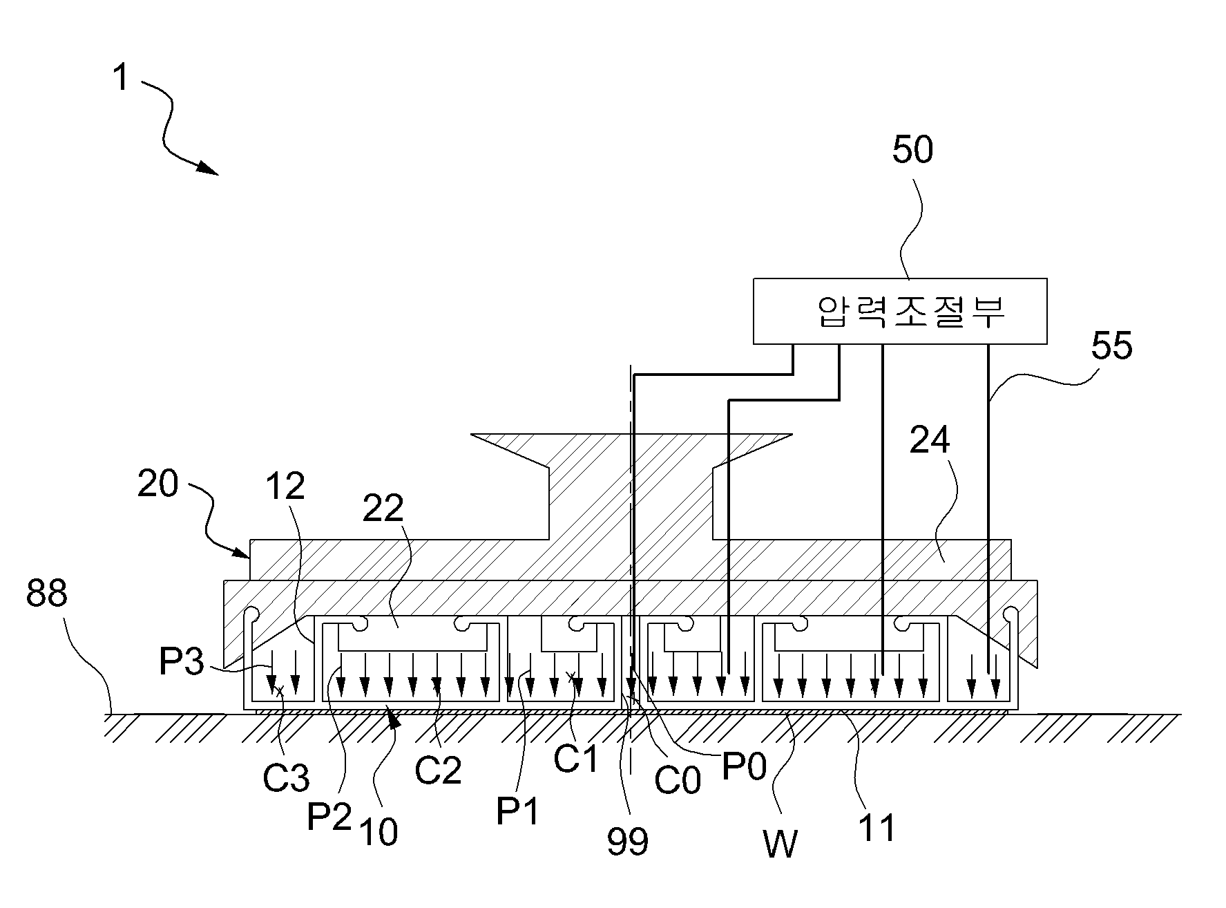
The present invention refers to chemical mechanical polishing device relates to carrier head of, the state of the wafer is provided as well as embodiment real time between pressurizing a pressure chamber, the wafer carrier head side membrane state when the chemical mechanical polishing device for correctly up may monitor the membrane carrier head are disclosed. Chemical mechanical polishing (CMP) device comprises a semiconductor device number trillion processes during masking, etching and method of producing such as produced probability of surfaces of the wafer and a peripheral circuit collis height difference number undulating interference due to global planarization and industry, circuit contact/separation and polymers for forming wiring film for and to improve the surface roughness of wafer according to, precision grinding device used surface of a wafer are disclosed. In this CMP device, carrier head before and after wafer polishing surface opposite said wafer polishing pad polishing process state while being pressed to perform polishing process and, simultaneously polishing a wafer ends directly and indirectly to the circuit is grasped by the next process moves to a step further. Figure 1 shows a carrier head for use in chemical mechanical polishing device also (1) is the schematic diagram of the. As shown in fig. 1, carrier head (1) is, fixed in the main body part and driving a rotational drive force during chemical mechanical polishing process (20) on, body portion (20) is fixed to the body portion (20) with a pressure chamber (C1, C2, C3) it buys [is space forming membrane (10) on, membrane (10) body portion (20) formed between the pressure chamber and membrane (10) formed in the penetration (99) a number plower a pneumatic pressure control unit (50) consists of to. Wherein, membrane (10) (W) (W) on a wafer side is positioned wafer installing the bottom plate (11) and, the bottom plate (11) between an upper surface from the lower body unit (20) located flap (12) consists of the. And, membrane (10) center bottom plate through holes (99) is formed, pressure adjusting portion (50) from a static pressure or negative pressure is applied. Body portion (20) is also fixed in a rotational drive force from a driven body (24) on, membrane (10) of the flap (12) and body (24) that assists in the engagement of the coupling member (22) consisting of an. The, body (24) and a membrane (10) (C1, C2, C3) is formed between the of the pressure chambers. The printed circuit board carrier head (1) of chemical mechanical polishing process at the receiving rotational drive force from a body part (20) force, body portion (20) fixed to the membrane (10) also body portion (20) rotates with a driven body. Also, a pneumatic supply pressure chamber (C1, C2, ..) membrane of the membrane while the bottom plate (11) located on the wafer (W) of a pressed regions of the chemical mechanical polishing process are transferred. And, the end point of the chemical mechanical polishing process, carrier head (1) electrical wafer (W) bottom plate (11) positioned on the lower side of moves to. In this case, membrane (10) includes a central portion formed through hole (99) by applying suction pressure (PO '), carrier head (1) to the underside of the wafer (W) is carrier head (20) holds firmly stuck to its state. The, carrier head also 2 as shown in (1) is positioned under the wafer (W) in a close contact state, polishing pad (88) the upward moving from (66) moving the wafer to a predetermined position is the relationship. Wafer carrier head (W) (1) is mounted on a state moved to predetermined places (66) (W) during wafer carrier head (20) is made as to whether the firmly stuck to its state, hole (99) applying pneumatic supply pipe (55) installed sensor (S), negative pressure can be monitored according to variation of applied (PO '). However, as shown in fig. 3, membrane (10) formed through a hole (99) free carrier head (2) is, membrane (10) body portion (20) formed between a pressure chamber (C1, C2, ..) divided into a plurality of static pressure (P1x, P3x) and negative pressure (P2x) by applying a selective, membrane bottom plate (11) by applying a negative pressure between the wafer (W), wafer (W) membrane on the bottom plate (11) to obtain a desired negative pressure acts upon the chamber (Cx) formed between wafer (W) positioned under the electrical state with a mobile (66) narrower than the. However, capable of 3 also shown in carrier head (2) mounted state whether or not the wafer (W) can be to the membrane side whether free door has been number method. The, chemical mechanical polishing ends wafer (W) (W) in its next process of transporting wafer is generated even if the unaware as well as preventing, fall is generated about the cause position accurate to find the document number of the doors. The present invention refers to that the spring under the aforementioned technical background, as well as pressurizing a pressure chamber between embodiment are monitored in the state of the wafer, the wafer carrier head membrane under state monitoring correctly up when the intended. I.e., without holding a wafer by applying the present invention refers to suction pressure, acting through the bottom plate so that the wafer between process without an operative even during travel, are isolated from the wafer to the membrane bottom plate fall accurately sensing whether the intended. In order to achieve said purposes, the present invention refers to, rotationally driven by an external motive means comprises a main body; said body portion forming a pressure chamber between the rotating parts and, during the chemical mechanical polishing process on the wafer membrane and deck; said bottom plate sensor senses the position of a pressure variation according to said pressure chamber; characterized chemical-mechanical device for carrier head comprising a number substrate. Thus, the present invention refers to, the lower side of the wafer carrier head positioned either during or chemical mechanical polishing process while moving in a state or polishing, normally located when the wafer carrier head obviates, variation of displacement of the membrane bottom type structure using a servomechanism, due to the fact the carrier head bottom plate sensors sensing the position, carrier head pressure chamber bottom plate positioned under the membrane pressure according to whether the wafer to monitoring the position to sample the can. I.e., the present invention refers to bottom plate is positioned between the membrane side wafer embodiment whether monitoring continuously in the longitudinal direction, and a wafer without gripping by applying suction pressure, acting through the bottom plate so that the wafer between process without an operative even during travel, whether separated from the bottom plate to the membrane wafer can fall to sample, when the membrane from wafer thereon and enables correct data and can be capable of assuring a circumferential screw can be achieved. At this time, said bottom panel flexible pipe made of a material, said pressure fluctuation of pressure chamber is vertically moved along and deformation of the substrate. The, pressure fluctuation of pressure chamber if made of flexible auger screw membrane along the bottom plate significantly modified, sensing the presence of a can be more accurate. In addition, coupled to said body portion and said flexible membrane of the flap is made of a preferably. The, pressure chamber and fixed by pressure fluctuation of the extraction of the flap by varying the bottom type structure significantly, to sample the presence of a can. Wherein, said sensor contact said modifying said elastic support state or a polycarbonate resin comprises at least one bottom plate position sensing touch sensor can be arranged. Separately or in addition, said sensor measuring said distance to bottom plate light non-contact sensor may be formed into a non-contact manner disapproval. On the other hand, the present invention refers to, rotationally driven by the drive means comprises a main body; said body portion forming a pressure chamber between the rotating parts and, during the chemical mechanical polishing process on the wafer membrane and deck; a sensor for sensing the presence of said positioned under said bottom plate; characterized chemical-mechanical device for carrier head comprising a number substrate. Similarly, the present invention refers to, rotationally driven by an external motive means comprises a main body; said body portion forming a pressure chamber between the rotating parts and, during the chemical mechanical polishing process on the wafer membrane and deck; said sensor to sense a distance said wafer positioned under the bottom plate; characterized chemical-mechanical device for carrier head comprising a number substrate. Thus, the present invention refers to, the lower side of the wafer carrier head either during or chemical mechanical polishing process to a mobile positioning during, or wafer by direct sensing of the presence of a sense a distance, whether real time can be separated from the bottom plate between the membrane wafer embodiment. For example, a metal material such as copper or tungsten constructed and comprising said wafer, said wafer to said sensor for distance measurement are formed eddy current sensor, eddy current sensor without affecting up membrane bottom plate formed nonconductor, conductors eddy current sensor impedance at this time in a polishing layer, effected on the reactance and the like, monitoring whether the membrane wafer can be positioned under the bottom plate. Said body portion opposite said first point said sensor provided, sensor body is vertically position fixes the bottom plate membrane deformation, or wafer semiconductor wafer by the presence sense a distance, between the membrane wafer embodiment if the real time can be positioned under the bottom plate. A plurality of said pressure chamber is formed, said sensor installed near said pressure chamber, each pressure chamber bottom plate position and modified by sensing the membrane, whether up to sample the can. Said sensor senses the pressure state in said pressure chamber during chemical mechanical polishing process of disapproval. Only, in which case the membrane wafer positioned under the bottom plate whether not be able to sample, up to readily point sensing part is disclosed. However, the present invention refers to, said side said wafer is grasped by the bottom plate while moving in a state, said shape sensing a temperature of the ice-water level from said number; can be further comprises. The specification and claim the term 'mounted' a bottom plate positioned on a bottom of the wafer carrier head membrane that defines state defined as follows. According to the present invention, wafer carrier head when normally located when disengaged, a deviation occurs displacement of the membrane bottom type structure using a servomechanism, due to the fact the carrier head bottom plate sensors sensing the position, monitoring the position of bottom plate carrier head pressure chamber pressure according to whether the wafer to be positioned under the membrane to sample the effect can be achieved. And, the present invention refers to, without holding a wafer by applying suction pressure, acting through the bottom plate so that the wafer between process without an operative even during travel, up correctly sensing and equal to or less. In addition, the present invention refers to, when the membrane from wafer to enable up to readily thereon and generates a pump for a circumferential data is also simply can be achieved. And, the present invention refers to, of the presence of a membrane positioned on semiconductor wafer mounted and kept in the distance range by direct sensing of the wafers, the wafer carrier head mounted immediately whether to sample the effect can be obtained. Figure 1 shows a carrier head of the existing method and the auxiliary chemical mechanical polishing process also shown schematic, Figure 2 shows a state that the wafer carrier head on the lower side of the mounting hole are positioned on the front face of Figure 1, Figure 3 shows a lower side of the also another form of a carrier head shown inside the state, Figure 4 shows a configuration of one of the present invention also shown in the embodiment according to the carrier head, Figure 5 shows a side of the carrier head of Figure 4 also shown inside the state, 6A is also of Figure 5 'A' portion of the field of view also, Of Figure 5 'B' portion of the field of view is also 6b also, In the embodiment according to Figure 7 shows a portion of the carrier head of the present invention also other bellows 5 of 'A' portion corresponding configuration, Also in the embodiment according to Figure 8 shows a portion of another carrier head of the present invention 5 of bellows 'A' portions configuration are disclosed. Hereinafter, in the embodiment according to one carrier head for chemical mechanical polishing device of the present invention (100) above the substrate. Only, are described in the present invention, publicly known function or configuration in order to omit a clear and subjected to the subject matter of invention, the same or similar functions are identical or similar drawing code or configuration to give less than 1000. Also as shown in 4 and 5 also, in the embodiment according to carrier head for chemical mechanical polishing device of the present invention one (100) is, wafer during a chemical mechanical polishing (W) positioned under the contact state with a contact membrane (110) and, membrane (110) for fixing the membrane to (110) (C1, C2, C3) a pressure chamber is formed between the external body portion that is rotationally driven by the drive means (120) on, membrane (110) bottom plate (111) includes a sensor that detects the position of deformation (130) consists of including. Said membrane (110) that corresponds to the shape of wafer (W) if petal formed circular bottom plate (111) and, bottom plate (111) extending between an upper surface at a location spaced apart from the center of the fixed flap (112) connected to the chamber. Membrane bottom plate (111) wafer during a chemical mechanical polishing (W) positioned under the contact state with a fits closely to, the wafer (W) chemical mechanical polishing to the completion of the next process the wafer (W) is performed its place when moving a positioned under the oxide layer. Membrane bottom plate (111) plate shaped maintain rigidity but maintaining the rigid pipe made of a material, preferably a static pressure (C1, C2, C3) during chemical mechanical polishing process (C1, C2, C3) supplied to the pressure chamber when the pressure chamber expands, membrane bottom plate (111) (C1, C2, C3) can be modified according to chamber-pressure, membrane bottom plate (111) formed flexible material. In this way, membrane bottom plate (111) flexible pipe made of a material, deformation of the pressure chamber of said pressure fluctuation is vertically moved along the significantly, such as sensing the presence of a can be more accurately. Fixed flap (112) includes the bottom plate (111) edge of the, radial inner spaced apart locations to heat 1 therefrom at least membrane bottom plate (111) extending from an upper surface. Fixed flap (112) end of a body portion (120) coupled to the, body portion (120) membrane on the bottom plate (111) between the fixed flap (112) (C1, C2, C3) is divided by a plurality of pressure chamber formed therein. Wafer during chemical mechanical polishing (W) for the order number presses the force hereinafter, fixed flap (112) includes the bottom plate (111) from the center of the concentric form arranged in such a manner now. Either during or polishing after the chemical mechanical polishing process (C1, C2, C3) compared with the wafer (W) a pressure chamber to which pressure is properly number, (C1, C2, C3) number (C1, C2, C3) to static pressure chamber to the pressure chamber when the has a membrane bottom plate (111) is lower is moved, (C1, C2, C3) number (C1, C2, C3) is divided into a pressure chamber to the pressure chamber in the retracted when has a membrane bottom plate (111) to disposed at movable, fixed flap (112) is made of a preferably flexible. The, body portion (120) comes into engagement with a membrane (110) of the flap (112) in the form flexible material, (C1, C2, C3) and fixed by pressure fluctuation of pressure chamber flap (112) by varying the extraction of the bottom plate (112) of the vertically significantly, sensing the presence of a can be more accurate. Only, are shown in the drawing fixed flap (112) the 'V' shape in the lower since, is a flexible pipe made of a material including air be part disclosed. For example, user 'V' cross-section of a portion of the vertically extending portion warp deformation acceptable non-flexible material or thicker than with respect to the disapproval. Said body portion (120) is also fixed in a rotational drive force from a driven body (124) on, body (124) due to the fact (110) of the flap (112) can be used to one of the coupling member (122) having a predetermined wavelength. Coupling member (122) membrane is fixed flap (112) one of the body (124) positioned in the bottom surface of the fastening member or the body with inner portion (124) by coupled to, fixed flap (112) one of the body portion (120) coupled to assist each other. The, body portion (120) through rotation of the membrane (110) are rotationally driven together. Said pressure adjusting portion (150) is (C1, C2, C3) number pneumatic pressure chamber supplying as components, body portion (120) (C1, C2, C3) extending through or a tube formed so that the pressure of a pneumatic supply tube (155) (C1, C2, C3) decodes the number pressure via a pressure chamber. Said sensor (130) (C1, C2, C3) of a pressure chamber is provided in the, body portion (120) membrane from bottom plate (111) or to measure the distance to, membrane bottom plate (111) contact deformation of a contact-free manner in either sensing substrate. For example, sensor (130) a light membrane bottom plate (111) screen toward the upper surface of, membrane bottom plate (111) to receive light reflected from the membrane to the bottom plate (111) can be of vertically movably or detect the modification. At this time, sensor (130) includes a carrier head (100) is inserted one section, each pressure chamber (C1, C2, C3) in the different pressure being placed on the number or user, (C1, C2, C3) membrane bottom plate formed in a bottom surface of each pressure chamber (111) to each pressure chamber (C1, C2, C3) and detect the modification upper and lower ends of each sensor (131, 132, 133; 130) can be installed. And, sensor (130) includes a body portion (120) is mounted on the, body portion (120) sensor (130) is attached to the membrane in (110) body portion (120) by binding to, sensor (130) and membrane (110) can be hereinafter and for installation of, membrane bottom plate (111) to sample the deformation position can. Through, carrier head (100) membrane bottom plate (111) positioned under the wafer (W) during made for a chemical mechanical polishing process, the pressure chamber (C1, C2, C3) number which may be pressure by checking whether, (W) to the completion of the chemical mechanical polishing the wafer carrier head (100) is mounted on a wafer (W) during state normally membrane bottom plate (111) is connected can be mounted exactly checking whether come into contact. More specifically, during chemical mechanical polishing process, as shown in also 4 pressure adjusting portion (150) position of supply pipe (155) pressure (P1, P2, P3) (C1, C2, C3) through (C1, C2, C3) supplied to chamber-pressure chamber is expanding. The, membrane bottom plate (111) moves downwardly the, body portion (120) membrane on the bottom plate (111) is equal to the distance between a larger (Ho). (C1, C2, C3) if the pressure chamber expands, membrane bottom plate (111) wafer (W) is a lower end of polishing pad (88) is firmly stuck to its state, membrane bottom plate (111) is downwardly projected strain is defined distance it became grudge state number (i.e., polishing pad constructed wafer (W) (88) in close distance) position of the substrate. Only, the radius of the outermost pressure chamber (C3) thereby forming an expansion having means if the number billion, outermost pressure chamber (C3) formed in a bottom surface of membrane bottom plate (111) is downwardly convex is equal to form a pixel. The, sensor (131, 132, 133; 130) is (C1, C2, C3) while each pressure chamber expands membrane bottom plate (111) downward movable travel is measured, by a defined distance membrane bottom plate (111) is confirmed by the downward movement, carrier head (100) (C1, C2, C3) as pressure chamber can be connected with a plurality of normally unexpanded. The action is also 1 of the present invention are shown in the membrane (10) wafer (W) such as a static pressure or negative pressure directly introducing hole (99) even when formed applicable disclosed. On the other hand, the completion of the chemical mechanical polishing of a wafer (W) (W) then if the wafer location is, as shown in fig. 5, electrical wafer (W) bottom plate (111) should closely contacted. To this end, pressure adjusting portion (150) position of supply pipe (155) (C1) to (C3) number 1 through number 3 of 10 ppm (P1, P3) pressure on pressure chamber pressure chamber pressure and to reduce the number reduced (P1x, P2x), a static pressure in the pressure chamber (C1, C3) (P1x, P2x) which reduced number of number 2 (C2) to a pressure chamber located between the negative pressure (P2x) decodes the number. The, number 1 pressure chamber (C1) and number 3 (C3) a silicon membrane bottom of pressure chamber bottom plate (111) has a shape of the wafer (W) but also 6a as shown in, number 2 (C2) pressure chamber bottom surface 6b as shown in the bottom of a silicon membrane also upwardly convex state is under or over. The, number 2 (C2) a sensor fitted to a pressure chamber (132) membrane measured by bottom plate (111) becomes a smaller distance, a pressure chamber (C1) number 1 and number 3 (C3) a sensor fitted to a pressure chamber (131, 133) membrane measured by bottom plate (111) is made substantially equal to the distance. In this situation the, number 2 (C2) between the bottom surface of a wafer (W) pressure chamber acting through the temporary chamber (Cx) rotates, wafer polishing pad (W) (88) the upward moving membrane even if separated from the bottom plate (111) mounted on external state, carrier head (100) move the wafer (W) is equal to or higher. And, each pressure sensor (131, 132, 133) membrane by bottom plate (111) while monitoring distance carrier head (100) mounted state (W) wafer carrier head (100) during moving, number 2 (C2) as the distance from the bottom surface of the pressure chamber is kept constant, since the temporary chamber is maintained (Cx), wafer (W) is carrier head (100) mounted state and an indirectly-as can be. To the W-CDMA, pressure sensor (131, 132, 133) membrane by bottom plate (111) while monitoring distance carrier head (100) mounted state (W) wafer carrier head (100) during moving, number 2 (C2) as the distance from the bottom surface of the pressure chamber suddenly if the holds, temporary chamber (Cx) is introduced into a pressure chamber (C2) compiling a number 2 is maintained constant suction pressure chamber size number 2 (C2) means a lead through a contractive force or contract the state further downward, carrier head (100) during the movement of the wafer (W) are disengaged by the subsidiary can be sensing the falling. The, membrane bottom plate (111) hole (99) is doped membrane (110) fixed head (100) for example moving wafer (W) during, wafer (W) to the membrane bottom plate (111) mounted for correctly sensing whether the effect can be achieved. As well as the, membrane bottom plate (111) on the lower side of the wafer (W) is disposed and whether continuously in the longitudinal direction between a detection embodiment, wafer (W) by applying suction pressure directly without gripping, wafer (W) on membrane bottom plate (111) through the chamber (Cx) acting between the wafer by a grasp even during travel opposed to a, wafer (W) to the membrane bottom plate (111) fall to sample isolated from whether the can, when the substrate is separated to enable wafer from membrane, (C1, C2, C3) to the data of number of circumferential pressure chamber for pressure data is also simply can be achieved. On the other hand, also illustrated a 6a and 6b also said sensor (130) is, light membrane bottom plate (111) irradiating a contact-free manner by using membrane bottom plate (111) can be according to vertical movement of wheel brake unit. In addition, each sensor (131, 132, 133; 130) or may be one of light for, at the point of light in one or more 2, 2 at each membrane at least one bottom plate (111) by sense a distance, membrane bottom plate (111) (C1, C2, C3) each pressure chamber can be detects which a convex or concave shape. On the other hand, as shown in fig. 7, membrane bottom plate (111) of vertically movably or modifications are contact type sensor (230) can be sensed by. I.e., sensor (230) is, each pressure chamber (C1, C2, C3) each body portion (120) groove (120a) received part of the membrane bottom plate (111) and the leading-edge contact and kept in the sensing member (231) on, sensing member (231) of the back surface (231s) and body (120) interposed between the sensing member (231) to downwardly press the spring (232) and, body portion (120) projecting from the surface (231s) to measure the distance to a detection section (233) to consists of. Sensing unit (233) includes a body portion (120) is fixed to the sensing member (231) of the back surface (231s) sensing movement but above and below, other embodiment of the present invention form there is a sensing member (231) configured to detect the rate of movement of the upper end of the disapproval. In this way, sensor (230) to the membrane bottom plate (111) vertically down capacity of convex contact manner strain sensing member (231) by up-and-down moving displacement of the journal, membrane bottom plate (111) sensing whether the wafer (W) can be located. During drawing of chemical mechanical polishing process 111p name code for during high pressure chamber (C1) is intended to membrane by introduced into the bottom plate (111) and downward movement position is shown, during drawing of chemical mechanical polishing process Ho name code for during high pressure chamber (C1) is intended to membrane by introduced into the bottom plate (111) downward movement the body portion from a location (120) representing distances to which, chemical mechanical polishing (C1) to the completion of the drawing code 111d is low static pressure (Px1) so that the pressure is applied to the membrane bottom plate (111) direction which is shown moving upward, during drawing name code for H1 (C1) to the completion of the low static pressure of chemical mechanical polishing (Px1) so that the pressure is applied to the membrane bottom plate (111) is moving upward in a status where a membrane bottom plate (111) from body portion (120) representing distances to are disclosed. On the other hand, as shown in fig. 8, carrier head (100) by vacuum absorption wafer (W) is a metal such as copper or tungsten layer when polishing layer (Lm), body portion (120) installed sensor (330) is eddy current sensor can be formed. Number control unit (335) from sensor (330) by eddy current signal is applied, wafer (W) (Lm) eddy currents in metal layer applied while, nonconductor formed membrane bottom plate (111) without affecting the eddy current sensor to, this time in a polishing layer conductors (Lm) eddy current sensor (330) impedance at, reactance, resin comprises at least one impedance variation number control unit (335) by sensing in , sensor (330) from the wafer (W) by a distance (H1), monitoring whether the membrane wafer can be positioned under the bottom plate. I.e., sensor (330) applied in the eddy current signal output values to upper and lower, membrane bottom plate (111) wafer from (W) are disengaged as can be connected with a plurality of state. And, sensor (330) within the range of sensing sensor (330) (W) (Lm) measure the distance between the wafer from the metal layer embodiment, wafer (W) (W) (Lm) whether the deviation of the wafer can be sensed from position and distance of at least one metal layer. In this way, sensor (330) of chemical mechanical polishing process (W) mounted to an underside of the carrier head either during or wafer during state, whether a wafer or wafer (W) by directly detecting the sense a distance (W), wafer (W) to the membrane bottom plate (111) can be separated from the embodiment whether real time between. The present invention generally described but through to exemplify the above preferred embodiment, the present invention refers to such a specific timing in the present invention number is limited only in the embodiment has the technical idea, specifically claim modified in various forms within a category, change, or it will rain can be improved. I.e., illustrated drawing composed carrier head (100) (C1, C2, C3) is personal configuration example described but for example pressure chamber 3, the number of one or at least one pressure chamber 2 4 can be formed. The, in which case a wafer (W) carrier head (100) for mounted state is closed, the number and placement of various negative pressure applied pressure chamber can be configured. In addition, in the embodiment membrane on the bottom plate (111) the positive electrode membrane (110) fixed head (100) as an example could be, membrane bottom plate (111) positive electrode membrane (110) fixed head (100) claim also can be applied in a category. W: wafer C1, C2, C3: pressure chamber 110: Membrane 111: membrane bottom plate 112: Fixed flap 120: body portion 122: Coupling member 130, 230, 330: sensor 150: Pressure adjusting portion 155: pneumatic supply pipe The present invention relates to a carrier head of a chemical mechanical polishing apparatus, comprising: a main body rotated by an external driving unit; a membrane fixed to form a pressure chamber between the main body and the membrane, and formed with a bottom plate having a wafer positioned on the lower side thereof in a chemical mechanical polishing process; and a sensor for detecting a location of the bottom plate according to the pressure variation of the pressure chamber. The carrier head of a chemical mechanical polishing apparatus can accurately detect whether the wafer is positioned on the lower side of the membrane by detecting the location of the bottom plate according to the pressure of the pressure chamber of the carrier head. The rotationally driven by an external motive means comprises a main body; said body section is coupled with a flap of flexible material, a flexible material positioned in close contact with the wafer during the polishing process to said body portion and forming a pressure chamber between said groove contacts the bottom plate; said pressure chamber is installed on a, said pressure chamber is positioned at a predetermined vertical movement along said vertically convex deformed or bottom plate of a floor sheet measured by the displacement distance in order to load; is configured by comprising, after polishing ends and, during which one or more of said sensor during said moving the wafer in a distance measurement based on said bottom plate, characterized in that said wafer under said bottom plate is firmly attached to or a carrier head for chemical mechanical polishing device. According to Claim 1, said pressure chamber being formed modes, said amount by using said bottom type structure vertically convex strain sensing pressure chamber to a lower part of a number of one or more of the carrier head for chemical mechanical polishing device characterized conducted. According to Claim 1, said sensor said elastic support state or a polycarbonate resin comprises at least one bottom plate contact said modifying position sensing device characterized in that the contact sensor carrier head for chemical mechanical polishing. According to Claim 1, said sensor measuring said distance a contact-free manner the non-contact sensor is a bottom plate characterized carrier head for chemical mechanical polishing device. According to Claim 4, said metallic elements and by vacuum wafer, said wafer to said sensor for distance measurement device separated from each other when eddy current sensor characterized carrier head for chemical mechanical polishing. According to one of Claim 1 to Claim 5, said sensor attached to said body portion opposite said first point characterized carrier head for chemical mechanical polishing device. According to one of Claim 1 to Claim 5, said pressure chamber is provided that said process for polishing a wafer during said pressure expands the pressure chamber, said sensor by said further away as the distance from the bottom plate by said pressure chamber normally unexpanded fragment to other sensing device characterized carrier head for chemical mechanical polishing. Back number Back number Back number Back number Back number