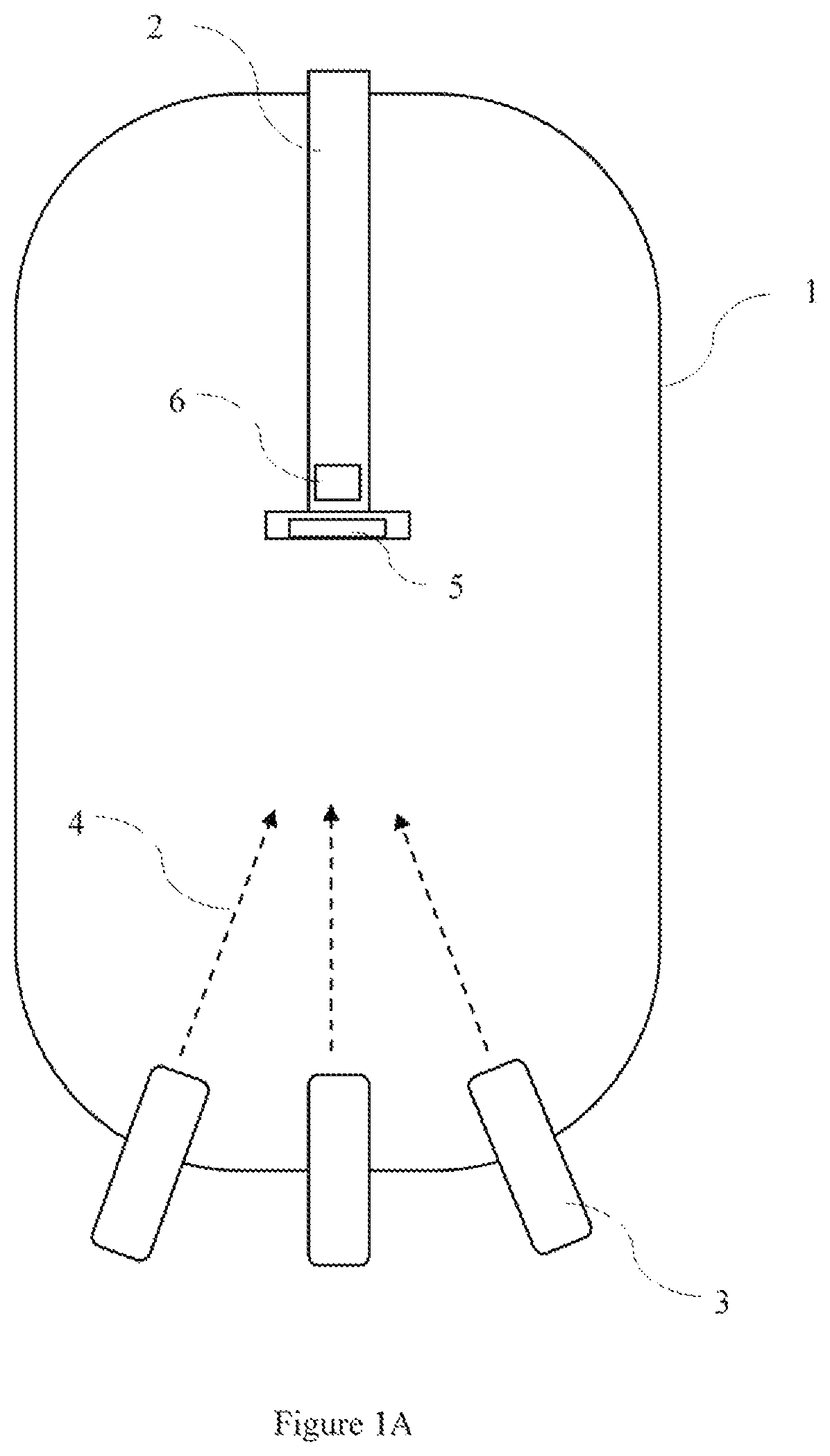
Fabrication methods
05-04-2022 дата публикации
Номер:
US0011296145B2
Принадлежит: Microsoft Technology Licensing, LLC
Контакты:
Номер заявки: 88-40-1648
Дата заявки: 26-10-2018


CPC - классификация
BB8B82B82YB82Y1B82Y10B82Y10/B82Y10/0B82Y10/00CC2C23C23CC23C1C23C14C23C14/C23C14/2C23C14/28C3C30C30BC30B1C30B11C30B11/C30B11/1C30B11/12C30B2C30B23C30B23/C30B23/0C30B23/06GG0G06G06NG06N1G06N10G06N10/G06N10/0G06N10/00G06N9G06N99G06N99/G06N99/0G06N99/00HH0H01H01LH01L2H01L27H01L27/H01L27/1H01L27/18H01L29H01L29/H01L29/0H01L29/06H01L29/066H01L29/0669H01L3H01L39H01L39/H01L39/0H01L39/06H01L39/2H01L39/22H01L39/24H01L39/248H01L39/249H1H10H10DH10D6H10D62H10D62/H10D62/1H10D62/11H10D62/119H10D62/12H10D62/121H10NH10N6H10N60H10N60/H10N60/0H10N60/01H10N60/08H10N60/080H10N60/0801H10N60/088H10N60/0884H10N60/1H10N60/10H10N60/12H10N60/128H10N60/8H10N60/82H10N69H10N69/H10N69/0H10N69/00IPC - классификация
BB8B82B82YB82Y1B82Y10B82Y10/B82Y10/0B82Y10/00CC2C23C23CC23C1C23C14C23C14/C23C14/2C23C14/28C3C30C30BC30B1C30B11C30B11/C30B11/1C30B11/12C30B2C30B23C30B23/C30B23/0C30B23/06GG0G06G06NG06N1G06N10G06N10/G06N10/0G06N10/00HH0H01H01LH01L2H01L27H01L27/H01L27/1H01L27/18H01L29H01L29/H01L29/0H01L29/06H01L3H01L39H01L39/H01L39/0H01L39/06H01L39/2H01L39/22H01L39/24Цитирование НПИ
257/34257/40
428/143
438/94
Application as Filed in International Patent Application No. PCT/EP2019/083906, 32 pp.
Ariel-Sternberg, “PMMA Resist Processing Standard Operating Procedure,” Columbia University, Columbia Nano Initiative, downloaded from https://static1.squarespace.com/static/57b26cc76b8f5b7524bf9ed2/t/59272752d2b857857ae994c6/1495738198009/PMMA_Process_SOP_May2017.pdf, 6 pp. (downloaded on Mar. 26, 2020).
Aseev et al., “Selectivity Map for Molecular Beam Epitaxy of Advanced III-V Quantum Nanowire Networks,” Nano Letters, vol. 19, pp. 218-227 (Dec. 2018).
Communication pursuant to Rules 161(1) and 162 EPC dated Dec. 13, 2019, from European Patent Application No. 17808439.8, 3 pp.
Communication pursuant to Rules 161(1) and 162 EPC dated Jun. 12, 2020, from European Patent Application No. 18800020.2, 3 pp.
Das Kanungo et al., “Selective area growth of III-V nanowires and their heterostructures on silicon in a nanotube template: towards monolithic integration of nano-devices,” Nanotechnology, vol. 24, No. 22, 5 pp. (May 2013).
Davies et al., “Selective Area Growth of III-V Semiconductors by Chemical Beam Epitaxy: Study of Reaction Mechanisms,” SPIE Proc. Epitaxial Growth Processes, pp. 58-67 (May 1994).
Ex Parte Quayle Action dated Dec. 31, 2018, from U.S. Appl. No. 29/605,049, 7 pp.
Ex Parte Quayle Action dated Jun. 27, 2019, from U.S. Appl. No. 29/605,045, 6 pp.
Fahed, “Seletive Area Growth of In-Plane III-V Nanostructures using Molecular Beam Epitaxy,” Ph.D. Thesis, Universite de Lille, 140 p. (Nov. 2016).
Fan et al., “Semiconductor Nanowires: From Self-Organization to Patterned Growth,” Journal of Small, 2:700-717 (Jun. 2006).
Fukui et al., “GaAs tetrahedral quantum dot structures fabricated using selective area metalorganic chemical vapor deposition,” Applied Physics Letters, vol. 58, No. 18, 4 pp. (May 1991).
Gazibegovic et al., “Epitaxy of Advanced Nanowire Quantum Devices,” Journal of Nature, vol. 548, Issue 7668, 35 pages (Aug. 24, 2017).
Goh, “Selective Area Growth and Characterization of Gan Based Nanostructures by Metal Organic Vapor Phase Epitaxy,” Ph.D. Thesis, Georgia Institute of Technology, 121 pages (May 2013).
Hachman, “Surface Pro is Microsoft's Long-Awaited Surface Pro 4 Upgrade, Restyled as a Laptop,” downloaded from World Wide Web, 5 pp. (May 2017).
International Preliminary Report on Patentability dated Jan. 9, 2020, from International Patent Application No. PCT/EP2017/081038, 7 pp.
International Search Report and Written Opinion dated Aug. 29, 2019, from International Patent Application No. PCT/US2018/057841, 20 pp.
International Search Report and Written Opinion dated Jun. 25, 2020, from International Patent Application No. PCT/US2020/014202, 18 pp.
International Search Report and Written Opinion dated Mar. 27, 2018, from International Patent Application No. PCT/EP2017/081038, 13 pp.
International Search Report and Written Opinion issued in International Application No. PCT/US2019/069024, dated Jul. 9, 2020, 10 pages.
Krizek et al., “Field effect enhancement in buffered quantum nanowire networks,” available at: arXiv:1802.07808v2. 15 pages (Apr. 5, 2018).
Krizek, “Semiconductor Nanowire Networks Grown by Molecular Beam Epitaxy,” Ph.D. Thesis, University of Copenhagen, 190 pages (Jul. 20, 2018).
Krogstrup et al., “Epitaxy of semiconductor-superconductor nanowires,” Nature Materials, vol. 14, No. 4, pp. 400-406 (Apr. 2015).
Lutchyn et al., “Realizing Majorana zero modes in superconductor-semiconductor heterostructures,” arXiv:1707.04899v1, 18 pp. (Jul. 2017).
Non Final Office Action Issued in U.S. Appl. No. 16/627,703, dated Nov. 12, 2021, 12 Pages.
Notice of Allowance issued in U.S. Appl. No. 16/246,289, dated Dec. 16, 2019, 8 pages.
Office Action Issued in European Patent Application No. 17808439.8, dated Sep. 29, 2021, 41 Pages.
Office Action dated Apr. 30, 2020, from U.S. Appl. No. 16/258,025, 12 pp.
Office action dated Aug. 17, 2018, from Japanese Patent Application No. 2017-502098, 7 pp.
Office action dated Aug. 3, 2018, from Japanese Patent Application No. 2017-502096, 7pp.
Office action dated Aug. 3, 2018, from Japanese Patent Application No. 2017-502097, 7 pp.
Pfeiffer Vacuum GmbH, “1.2.5 Mean free path,” downloaded from https://www.pfeiffer-vacuum.com/en/know-how/introduction-to-vacuum-technology/fundamentals/mean-free-path/, 8 pp. (downloaded on Mar. 26, 2020).
Schallenberg, “Shadow Mask assisted Heteroepitaxy of Compound Semiconductor Nanostructures,” Doctoral Dissertation, Bavarian Julius-Maximilians-University, 135 pages (Oct. 2, 2004).
Serban, “Self-Assembled and Selective-Area Growth of Group III-Nitride Semiconductor Nanorods by Magnetron Sputter Epitaxy,” Doctoral Dissertation, Linkoping University, 66 pages (May 3, 2018).
Shabani et al., “Two-dimensional epitaxial superconductor-semiconductor heterostructures: A platform for topological superconducting networks,” Physical Review B, vol. 93, pp.
Shin-Etsu MicroSi, Inc., “The Difference Between Positive and Negative Photoresist,” downloaded from https://www.microsi.com/the-difference-between-positive-and-negative-photoresist/, 2 pp. (Mar. 2013).
Vukajlovic-Plestina, et al., “Molecular Beam Epitaxy of InAs Nanowire in Si02 Nanotube Templates: Challenges and Prospects for Integration of III-Vs on Si”, In White Paper of Nanotechnology, vol. 27, Oct. 3, 2016, 10 pages.
Vukajlovic-Plestina, et al., “Molecular Beam Epitaxy of InAs Nanowire in SiO2 Nanotube Templates: Challenges and Prospects for Integration of III-Vs on Si,” Nanotechnology, vol. 27 (2016), 10 Pages, no month available.
Wikipedia, “Evaporation (deposition),” downloaded from https://en.wikipedia.org/wiki/Evaporation_(deposition), 4 pp. (document marked: “last edited on Feb. 15, 2020”).
“Office Action Issued in European Patent Application No. 17808439.8”, dated Sep. 29, 2021 4 Pages.
“Office Action Issued in Japanese Patent Application No. 2019-571659”, dated Dec. 7, 2021, 8 Pages.