LASER PROCESSING APPARATUS AND LASER PROCESSING METHOD
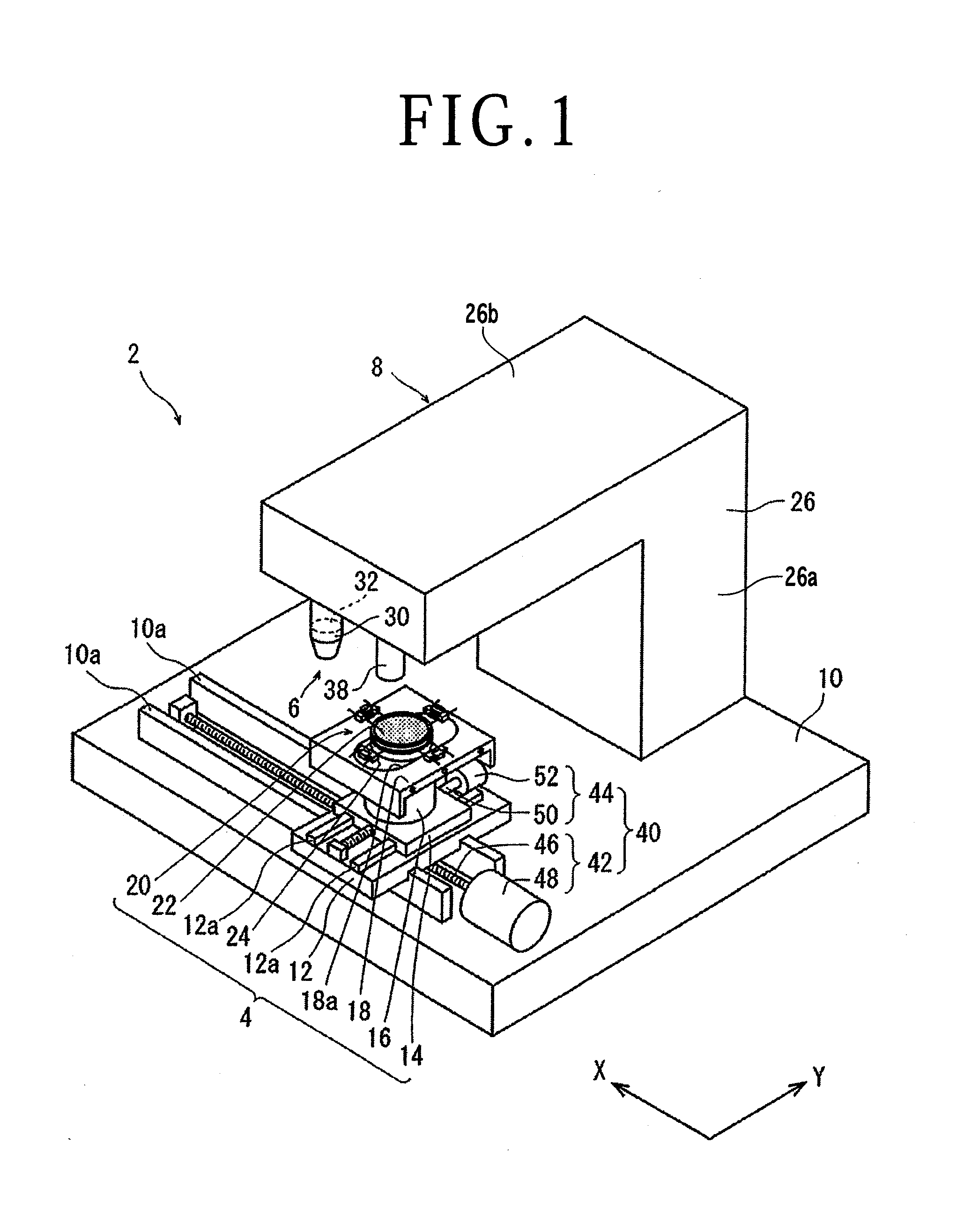
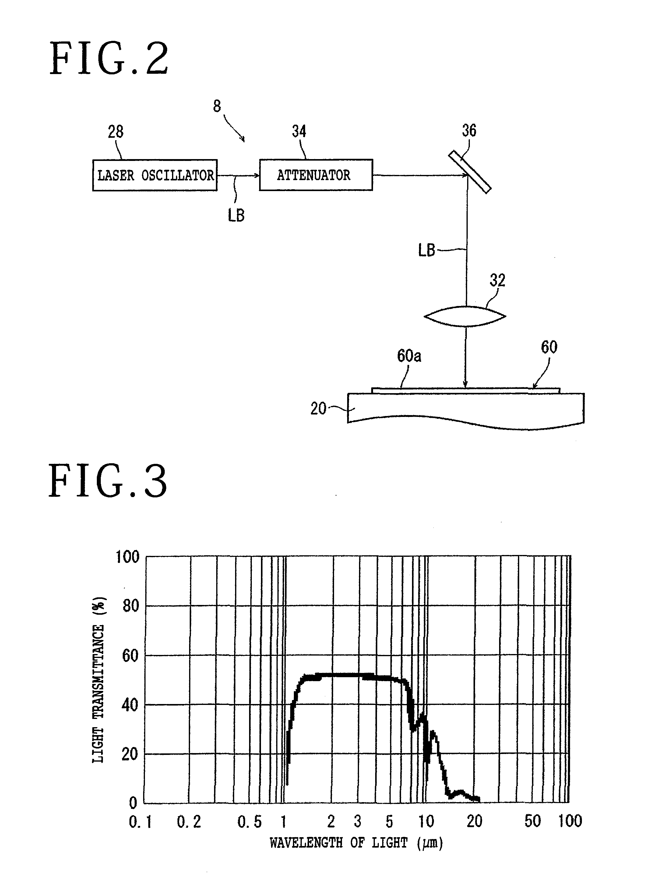
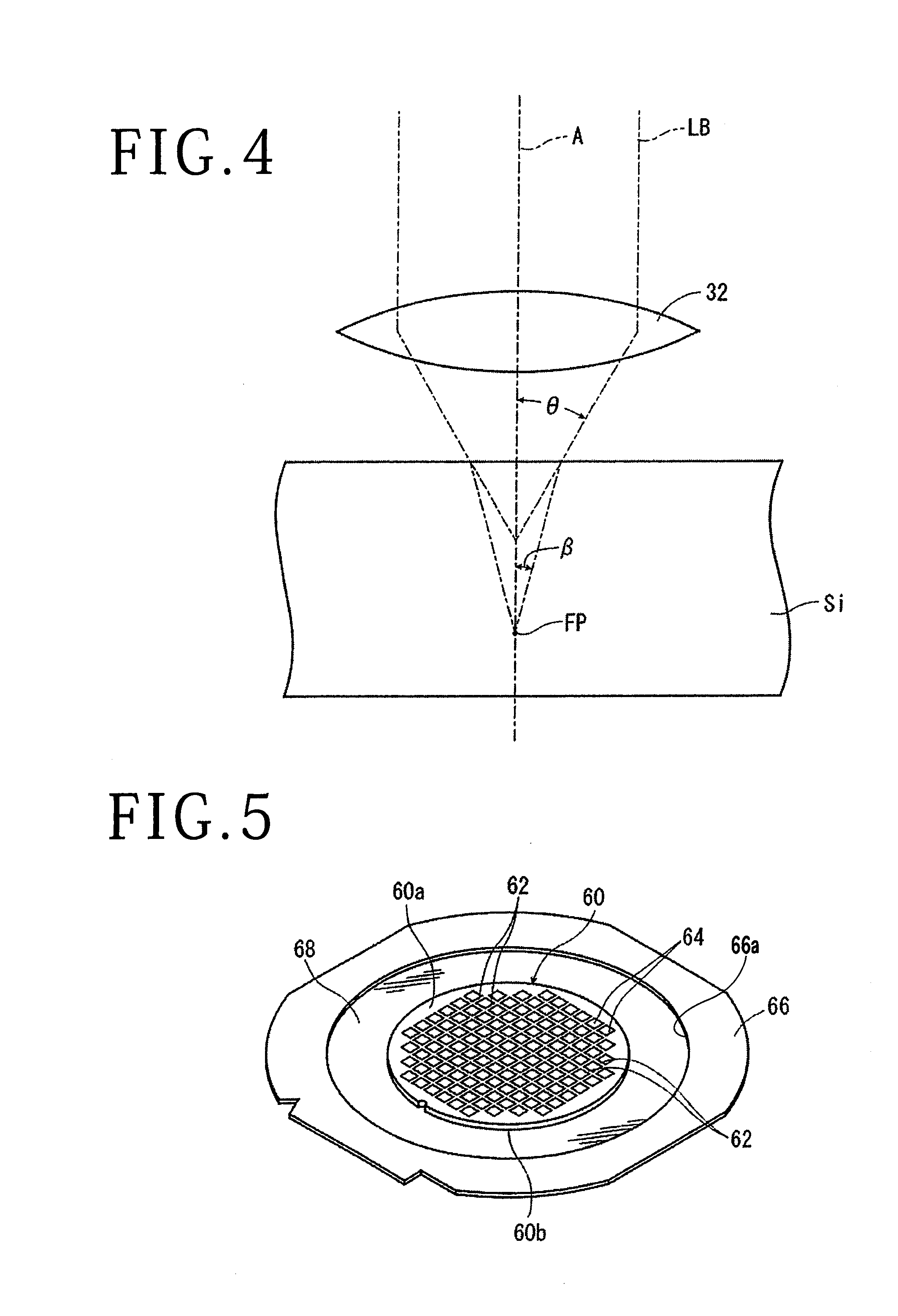
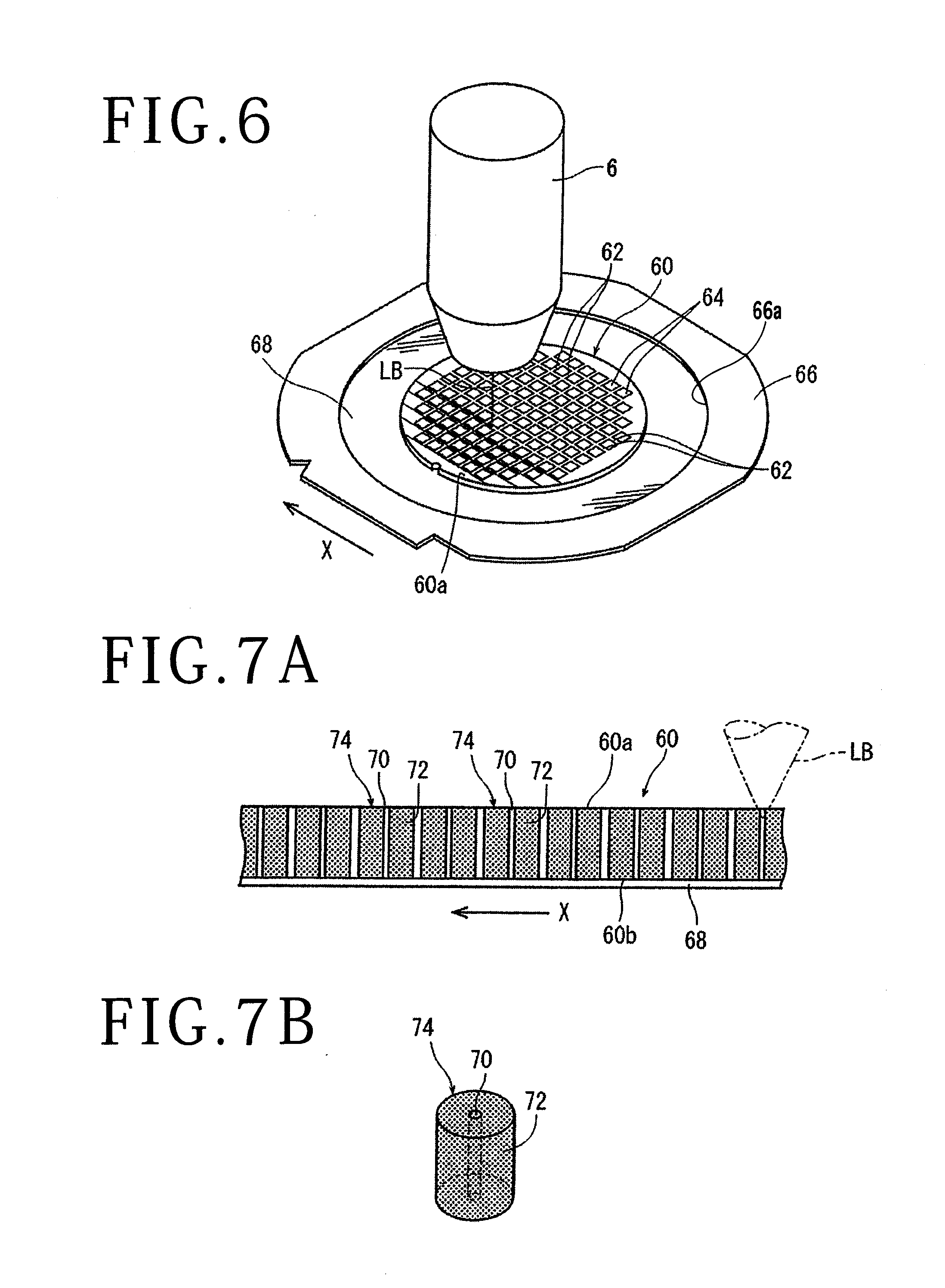
The present invention relates to a laser processing apparatus for forming shield tunnels in a single crystal silicon wafer, and also relates to a laser processing method for forming shield tunnels in a single crystal silicon wafer. A plurality of devices such as integrated circuits (ICs) and large scale integrated circuits (LSIs) are formed on the front side of a wafer so as to be separated by a plurality of crossing division lines formed on the front side of the wafer. The wafer thus having the plural devices on the front side is divided along the division lines into individual device chips by using a laser processing apparatus. The device chips thus obtained are used in various electric equipment such as mobile phones and personal computers. There are various types of laser processing methods using a laser processing apparatus. For example, the following types (1), (2), and (3) are known in the art. (1) A laser beam having an absorption wavelength to a workpiece is applied to the workpiece in the condition where the focal point of the laser beam is set on the upper surface of the workpiece, thereby performing ablation to form a groove as a division start point on the upper surface of the workpiece (see Japanese Patent Laid-Open No. 1998-305420, for example). (2) A laser beam having a transmission wavelength to a workpiece is applied to the workpiece in the condition where the focal point of the laser beam is set inside the workpiece, thereby forming a modified layer as a division start point inside the workpiece (see Japanese Patent No. 3408805, for example). (3) A laser beam having a transmission wavelength to a workpiece is applied to the workpiece in the condition where the focal point of the laser beam is set at a predetermined position inside the workpiece, thereby forming a plurality of shield tunnels as a division start point in the workpiece, in which each shield tunnel is composed of a fine hole and an amorphous region formed around the fine hole for shielding the fine hole, and the fine hole extends from the front side of the workpiece to the back side thereof (see Japanese Patent Laid-Open No. 2014-221483, for example). Japanese Patent Laid-Open No. 2014-221483 mentioned above states that sapphire (Al2O3), silicon carbide (SiC), and gallium nitride (GaN) were extracted as the material of a wafer to repeatedly conduct a test for determining the conditions that the shield tunnels can be properly formed. According to the result of this test, the wavelength of the laser beam to be applied to the wafer is set to 1030 nm and the numerical aperture of a focusing lens for focusing and applying the laser beam to the wafer is decided so that the value obtained by dividing the numerical aperture of the focusing lens by the refractive index of the material of the wafer falls within the range of 0.05 to 0.2. The present inventors conducted a test using single crystal silicon as the material of the wafer and applying the conditions disclosed in Japanese Patent Laid-Open No. 2014-221483 to the single crystal silicon wafer. However, it was found that proper shield tunnels cannot be formed in this case. It is therefore an object of the present invention to provide a laser processing apparatus which can form proper shield tunnels in a single crystal silicon wafer. It is another object of the present invention to provide a laser processing method which can form proper shield tunnels in a single crystal silicon wafer. In accordance with an aspect of the present invention, there is provided a laser processing apparatus including a chuck table for holding a workpiece; the workpiece including a single crystal silicon wafer; and a laser beam applying unit including focusing means having a focusing lens for applying a laser beam to the workpiece held on the chuck table to thereby process the workpiece; the laser beam applying unit further including a laser oscillator for oscillating a pulsed laser beam having a wavelength of 1950 nm or more in a transmission wavelength region to the single crystal silicon wafer as the laser beam. Preferably, the numerical aperture of the focusing lens is set so that the value obtained by dividing the numerical aperture of the focusing lens by the refractive index of single crystal silicon falls within the range of 0.05 to 0.2. In accordance with another aspect of the present invention, there is provided a laser processing method using a laser processing apparatus including a chuck table for holding a workpiece and a laser beam applying unit including focusing means having a focusing lens for applying a laser beam to the workpiece held on the chuck table to thereby process the workpiece, the laser processing method including a single crystal silicon wafer selecting step of selecting a single crystal silicon wafer as the workpiece; a laser beam selecting step of selecting a pulsed laser beam having a wavelength of 1950 nm or more in a transmission wavelength region to the single crystal silicon wafer as the laser beam; and a shield tunnel forming step of applying the pulsed laser beam to the single crystal silicon wafer along a predetermined area in the condition where the focal point of the pulsed laser beam is set inside the single crystal silicon wafer, thereby forming a plurality of shield tunnels arranged along the predetermined area, each shield tunnel being composed of a fine hole and an amorphous region formed around the fine hole for shielding the fine hole, the fine hole extending from a beam applied surface of the single crystal silicon wafer where the pulsed laser beam is applied to the other surface opposite to the beam applied surface. Preferably, the laser processing method further includes a numerical aperture deciding step of deciding the numerical aperture of the focusing lens so that the value obtained by dividing the numerical aperture of the focusing lens by the refractive index of single crystal silicon falls within the range of 0.05 to 0.2. According to the laser processing method of the present invention, proper shield tunnels can be formed in a single crystal silicon wafer. The above and other objects, features, and advantages of the present invention and the manner of realizing them will become more apparent, and the invention itself will best be understood from a study of the following description and appended claims with reference to the attached drawings showing a preferred embodiment of the invention. There will now be described a preferred embodiment of the laser processing apparatus according to the present invention, with reference to the drawings. Referring to As shown in The laser beam applying unit 8 will now be described with reference to The laser beam applying unit 8 will further be described with reference to The numerical aperture NA of the focusing lens 32 in the focusing means 6 is set so that the value S (S=NA/n) obtained by dividing the numerical aperture NA of the focusing lens 32 by the refractive index n of single crystal silicon falls within the range of 0.05 to 0.2 (0.05≤S≤0.2). The refractive index n of single crystal silicon is usually approximately 3.7. Accordingly, in the case that the refractive index n of single crystal silicon is 3.7, the numerical aperture NA of the focusing lens 32 is set in the range of 0.185 to 0.74 (0.185≤NA≤0.74). There will now be described the relation among the numerical aperture NA of the focusing lens 32, the refractive index n of single crystal silicon, and the value S (S=NA/n) obtained by dividing the numerical aperture NA of the focusing lens 32 by the refractive index n of single crystal silicon, with reference to As shown in Referring again to The laser processing method according to this preferred embodiment will now be described. In this preferred embodiment, a single crystal silicon wafer selecting step is first performed to select a single crystal silicon wafer as the workpiece. Further, a laser beam selecting step is performed to select a laser beam having a wavelength of 1950 nm or more in a transmission wavelength region to a single crystal silicon wafer. As described above, the laser oscillator 28 of the laser processing apparatus 2 is so configured as to oscillate a pulsed laser beam LB having a wavelength of 1950 nm or more in a transmission wavelength region to a single crystal silicon wafer. Accordingly, in the laser processing method using the laser processing apparatus 2, the laser beam selecting step is necessarily performed. Preferably, a numerical aperture deciding step is further performed to decide the numerical aperture of a focusing lens so that the value obtained by dividing the numerical aperture of the focusing lens by the refractive index of single crystal silicon falls within the range of 0.05 to 0.2. As described above, the numerical aperture NA of the focusing lens 32 in the focusing means 6 in the laser processing apparatus 2 is set so that the value S (S=NA/n) obtained by dividing the numerical aperture NA of the focusing lens 32 by the refractive index n of single crystal silicon falls within the range of 0.05 to 0.2 (0.05≤S≤0.2). Accordingly, in the laser processing method using the laser processing apparatus 2, the numerical aperture deciding step is necessarily performed. After performing the single crystal silicon wafer selecting step, the laser beam selecting step, and the numerical aperture deciding step, a shield tunnel forming step is performed to apply the pulsed laser beam LB to the single crystal silicon wafer 60 along each division line 62 in the condition where the focal point FP of the pulsed laser beam LB is set inside the wafer 60, thereby forming a plurality of shield tunnels arranged along each division line 62, each shield tunnel being composed of a fine hole and an amorphous region formed around the fine hole for shielding the fine hole, the fine hole extending from the front side 60 Thereafter, a laser beam applying step is performed to apply the pulsed laser beam LB to the wafer 60 along the predetermined division line 62 as relatively moving the wafer 60 and the focal point FP in the X direction, in which the pulsed laser beam LB has a wavelength of 1950 nm or more in a transmission wavelength region to the wafer 60. As shown in As described above, the laser processing apparatus 2 includes the laser oscillator 28 for oscillating the pulsed laser beam LB having a wavelength of 1950 nm or more in a transmission wavelength region to the single crystal silicon wafer 60. Accordingly, the shield tunnels 74 can be properly formed in the single crystal silicon wafer 60. Further, the laser processing method according to this preferred embodiment includes the single crystal silicon wafer selecting step of selecting the single crystal silicon wafer 60 as the workpiece, the laser beam selecting step of selecting the pulsed laser beam LB having a wavelength of 1950 nm or more in a transmission wavelength region to the single crystal silicon wafer 60, and the shield tunnel forming step of applying the pulsed laser beam LB to the single crystal silicon wafer 60 along each division line 62 in the condition where the focal point FP of the pulsed laser beam LB is set inside the wafer 60, thereby forming the plural shield tunnels 74 arranged along each division line 62, each shield tunnel 74 being composed of the fine hole 70 and the amorphous region 72 formed around the fine hole 70 for shielding the fine hole 70, the fine hole 70 extending from the front side 60 While the laser processing method using the laser processing apparatus 2 has been described in this preferred embodiment, the laser processing method according to the present invention is not limited to such a laser processing method using the laser processing apparatus 2, provided that the laser processing method essentially includes the single crystal silicon wafer selecting step, the laser beam selecting step, and the shield tunnel forming step. Further, in the above preferred embodiment, the front side 60 The present inventors conducted a test on the laser beam conditions for formation of proper shield tunnels in a single crystal silicon wafer. Such laser beam conditions will now be described according to the results of the test. A single crystal silicon wafer has a transmission of approximately 55% for infrared light in a predetermined wavelength region. In consideration of this fact, if a laser beam having a wavelength of 1030 nm near the absorption edge of single crystal silicon is used to form shield tunnels, the following possibility may be assumed. That is, in this case, a modified layer may be formed inside the single crystal silicon wafer by the transmission of the laser beam. However, the formation of shield tunnels may be hindered by the absorption of the laser beam, so that proper shield tunnels cannot be formed. Accordingly, the present inventors conducted the test under the conditions that the wavelength of the laser beam was set longer than the absorption edge of single crystal silicon. To find out the wavelength of a laser beam for the formation of proper shield tunnels in a single crystal silicon wafer, the present inventors performed laser processing under the following conditions. That is, the focal point of the laser beam was set inside the single crystal silicon wafer, and the laser beam was applied to the wafer as relatively moving the wafer and the focal point at a predetermined feed speed. To form each shield tunnel in the wafer, the focal point of the laser beam is formed so as to be dispersed in the direction of the thickness of the wafer. Accordingly, it is preferable to use a focal region in place of the focal point. The numerical aperture NA of the focusing lens was set in consideration of the test described in Japanese Patent Laid-Open No. 2014-221483 mentioned above, that is, the numerical aperture NA was set so that S=NA/n is in the range of 0.05 to 0.2 (0.05≤S≤0.2), where n is the refractive index of single crystal silicon. Since the refractive index of single crystal silicon is approximately 3.7, the numerical aperture NA was set so that S=NA/n=NA/3.7=0.135 holds. In this case, the numerical aperture NA of the focusing lens was set to 0.5. Thickness of the single crystal silicon wafer: 700 μm Wavelength of the pulsed laser beam: 1034 to 2200 nm Numerical aperture NA of the focusing lens: 0.5 Average power: 3 W Repetition frequency: 50 kHz Pulse width: 10 nanoseconds Feed speed: 500 mm/second It is apparent from the result of Test 1 that the wavelength of the laser beam capable of forming proper shield tunnels in the single crystal silicon wafer is 1950 nm or more in a transmission wavelength region to the single crystal silicon wafer. Further, in a wavelength region up to approximately 6000 nm, the light transmission of single crystal silicon is approximately 55% (see To find out the relation between the refractive index n of single crystal silicon and the numerical aperture NA of the focusing lens for the purpose of formation of proper shield tunnels in a single crystal silicon wafer, the present inventors performed laser processing under the following conditions. That is, the focal point of the laser beam was set inside the single crystal silicon wafer, and the laser beam was applied to the wafer as relatively moving the wafer and the focal point at a predetermined feed speed. Thickness of the single crystal silicon wafer: 700 μm Wavelength of the pulsed laser beam: 1950 nm Average power: 3 W Repetition frequency: 50 kHz Pulse width: 10 nanoseconds Feed speed: 500 mm/second It is apparent from the result of Test 2 that the relation between the refractive index n of single crystal silicon and the numerical aperture NA of the focusing lens allowing the formation of proper shield tunnels in the single crystal silicon wafer can be expressed as 0.05≤NA/n≤0.2. The present invention is not limited to the details of the above described preferred embodiment. The scope of the invention is defined by the appended claims and all changes and modifications as fall within the equivalence of the scope of the claims are therefore to be embraced by the invention. A laser processing method includes holding a single crystal silicon wafer as a workpiece, selecting a laser beam having a wavelength of 1950 nm or more in a transmission wavelength region to the single crystal silicon wafer, and applying the laser beam to the single crystal silicon wafer along a predetermined area with the focal point of the laser beam set inside the wafer, thereby forming a plurality of shield tunnels arranged along the predetermined area. Each shield tunnel is composed of a fine hole and an amorphous region formed around the fine hole for shielding the fine hole. The fine hole extends from a beam applied surface of the wafer where the laser beam is applied to the other surface opposite to the beam applied surface. 1. A laser processing apparatus comprising:
a chuck table for holding a workpiece, said workpiece including a single crystal silicon wafer; and a laser beam applying unit including focusing means having a focusing lens for applying a laser beam to said workpiece held on said chuck table to thereby process said workpiece; said laser beam applying unit further including a laser oscillator for oscillating a pulsed laser beam having a wavelength of 1950 nm or more in a transmission wavelength region to said single crystal silicon wafer as said laser beam. 2. The laser processing apparatus according to 3. A laser processing method using a laser processing apparatus including a chuck table for holding a workpiece and a laser beam applying unit including focusing means having a focusing lens for applying a laser beam to said workpiece held on said chuck table to thereby process said workpiece, said laser processing method comprising:
a single crystal silicon wafer selecting step of selecting a single crystal silicon wafer as said workpiece; a laser beam selecting step of selecting a pulsed laser beam having a wavelength of 1950 nm or more in a transmission wavelength region to said single crystal silicon wafer as said laser beam; and a shield tunnel forming step of applying said pulsed laser beam to said single crystal silicon wafer along a predetermined area in the condition where the focal point of said pulsed laser beam is set inside said single crystal silicon wafer, thereby forming a plurality of shield tunnels arranged along said predetermined area, each shield tunnel being composed of a fine hole and an amorphous region formed around said fine hole for shielding said fine hole, said fine hole extending from a beam applied surface of said single crystal silicon wafer where said pulsed laser beam is applied to the other surface opposite to said beam applied surface. 4. The laser processing method according to a numerical aperture deciding step of deciding the numerical aperture of said focusing lens so that the value obtained by dividing the numerical aperture of said focusing lens by the refractive index of single crystal silicon falls within the range of 0.05 to 0.2.BACKGROUND OF THE INVENTION
Field of the Invention
Description of the Related Art
SUMMARY OF THE INVENTION
BRIEF DESCRIPTION OF THE DRAWINGS
DETAILED DESCRIPTION OF THE PREFERRED EMBODIMENT
(Test 1)
(Result of Test 1)
1034 poor 1064 poor 1300 poor 1900 slightly good 1950 good 2000 good 2100 good 2200 good (Conclusion Based on Test 1)
(Test 2)
(Result of Test 2)
0.05 poor 0.014 0.1 poor 0.027 0.15 poor 0.041 0.2 good 0.054 0.25 good 0.068 0.3 good 0.081 0.35 good 0.095 0.4 good 0.108 0.45 good 0.122 0.5 good 0.135 0.55 good 0.149 0.6 good 0.162 0.65 good 0.176 0.7 good 0.189 0.75 good 0.203 0.8 poor 0.216 0.9 poor 0.243 (Conclusion Based on Test 2)