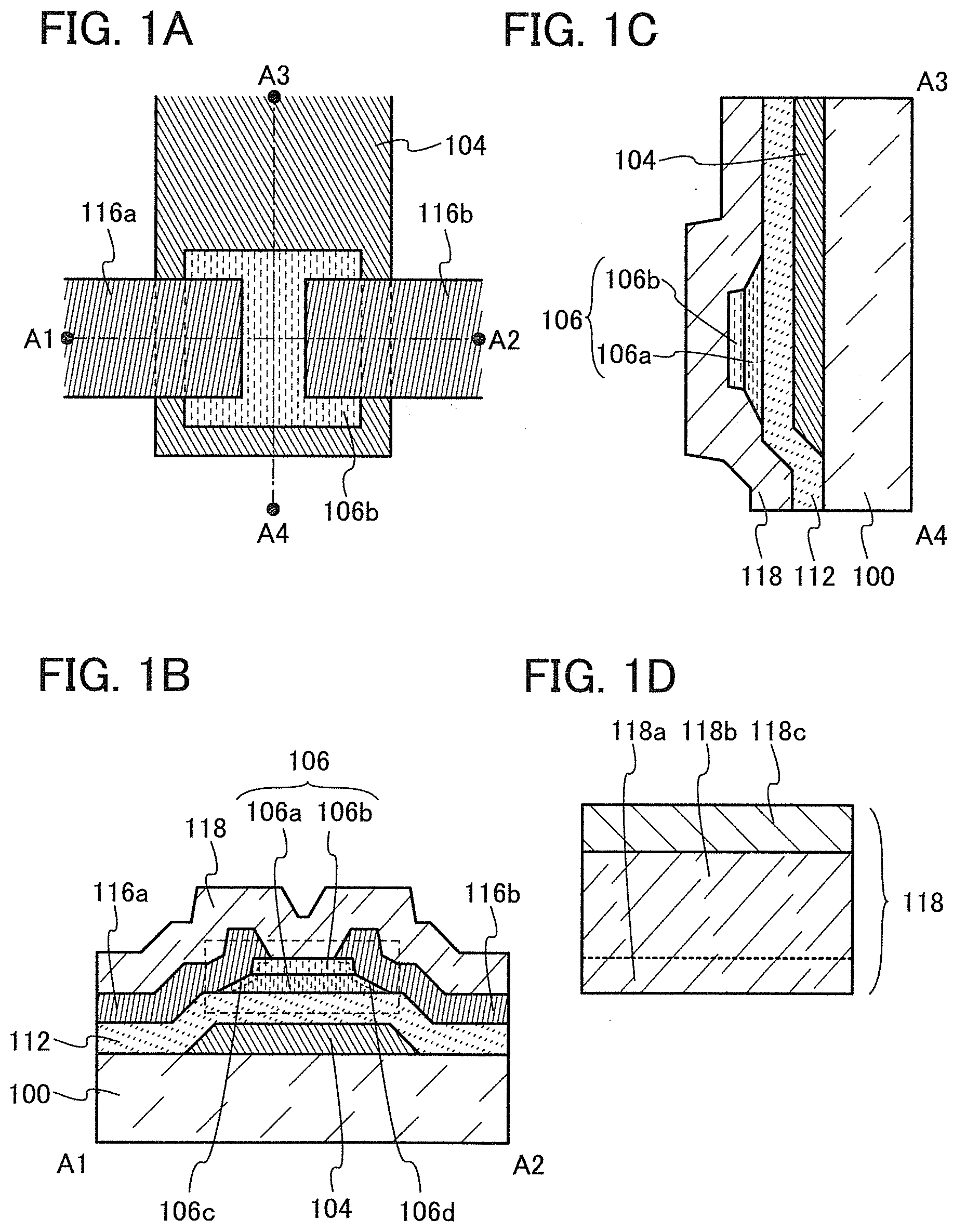
SEMICONDUCTOR DEVICE
The present invention relates to a semiconductor device and a manufacturing method thereof. A semiconductor device in this specification refers to any device that can function by utilizing semiconductor characteristics. An electro-optical device, a semiconductor circuit, an electronic appliance, and the like are all semiconductor devices. A technique for forming a transistor by using a semiconductor film formed over a substrate having an insulating surface has attracted attention. The transistor is applied to a wide range of semiconductor devices such as an integrated circuit and a display device. A silicon film is known as a semiconductor film applicable to the transistor. As the silicon film used as a semiconductor film of a transistor, either an amorphous silicon film or a polycrystalline silicon film is used depending on the purpose. For example, in the case of a transistor included in a large-sized display device, it is preferred to use an amorphous silicon film, which can be formed using the established technique for forming a film on a large-sized substrate. On the other hand, in the case of a transistor included in a high-performance display device where driver circuits are formed over the same substrate, it is preferred to use a polycrystalline silicon film, which can form a transistor having a high field-effect mobility. As a method for forming a polycrystalline silicon film, high-temperature heat treatment or laser light treatment which is performed on an amorphous silicon film has been known. Further, in recent years, an oxide semiconductor film has attracted attention. For example, a transistor which includes an oxide semiconductor film containing indium, gallium, and zinc and having a carrier density lower than 1018/cm3is disclosed (see Patent Document 1). An oxide semiconductor film can be formed by a sputtering method and therefore can be applied to a transistor in a large-sized display device. Moreover, a transistor including an oxide semiconductor film has a high field-effect mobility; therefore, a high-performance display device where driver circuits are formed over the same substrate can be obtained. In addition, there is an advantage that capital investment can be reduced because part of production equipment for a transistor including an amorphous silicon film can be retrofitted and utilized. A transistor including an oxide semiconductor film is known to have extremely low leakage current in an off state (also referred to as off-state current). For example, a CPU with low-power consumption utilizing the low leakage current of the transistor including an oxide semiconductor film is disclosed (see Patent Document 2). In a transistor including an oxide semiconductor film, defects generated in the oxide semiconductor film or defects generated at an interface between the oxide semiconductor film and an insulating film cause poor electrical characteristics of the transistor. With the expansion of the application range of a transistor including an oxide semiconductor film, reliability is being demanded in much more aspects. In view of this situation, it is an object of one embodiment of the present invention to provide a transistor including an oxide semiconductor film with stable electrical characteristics. It is an object of one embodiment of the present invention to provide a transistor including an oxide semiconductor film with excellent electrical characteristics. Further, it is an object of one embodiment of the present invention to provide a highly reliable semiconductor device including such a transistor. An embodiment of the present invention is a semiconductor device which includes a multilayer film in which an oxide semiconductor film and an oxide film are stacked, a gate electrode, and a gate insulating film. In the semiconductor device, the multilayer film overlaps with the gate electrode with the gate insulating film interposed therebetween. Further, the multilayer film has a shape having a first angle between a bottom surface of the oxide semiconductor film and a side surface of the oxide semiconductor film and a second angle between a bottom surface of the oxide film and a side surface of the oxide film. In addition, the first angle is an acute angle and smaller than the second angle. In the multilayer film of the above-described semiconductor device, an upper edge of the oxide semiconductor film may substantially coincide with a lower edge of the oxide film. In the multilayer film, the oxide film may be stacked over the oxide semiconductor film or alternatively may be formed over and below the oxide semiconductor film. In the semiconductor device, the first angle and the second angle are each preferably greater than or equal to 10° and less than 90°. In the above-described semiconductor device, the oxide film preferably includes an element in common with the oxide semiconductor film and has an energy of a bottom of a conduction band that is closer to a vacuum level than that of the oxide semiconductor film is. For example, it is preferable that the oxide semiconductor film and the oxide film include an In-M-Zn oxide (M is Al, Ga, Ge, Y, Zr, Sn, La, Ce, or Nd) and that the oxide film have a lower atomic ratio of In to M than the oxide semiconductor film. In the above-described semiconductor device, it is preferable that the oxide film be amorphous, the oxide semiconductor film be crystalline, and a c-axis of a crystal part included in the oxide semiconductor film be parallel to a normal vector of a surface of the oxide semiconductor film. In the above-described semiconductor device, a source electrode and a drain electrode may be provided in contact with the multilayer film. A low-resistance region may be provided in a region that is in the multilayer film and in the vicinity of an interface between the multilayer film and one of the source electrode and the drain electrode. In the above-described semiconductor device, an oxide film having the same or different composition as the oxide film may be provided in contact with a top surface of the source electrode, a top surface of the drain electrode, and a top surface of the multilayer film. With one embodiment of the present invention using a multilayer film including an oxide film and an oxide semiconductor film, a transistor can have stable electrical characteristics. Further, by forming the multilayer film in a tapered shape having at least the first angle and the second angle larger than the second angle, the contact area between the oxide semiconductor film serving as a channel region and the source and drain electrodes can be increased, whereby on-state current of the transistor can be increased. Further, with one embodiment of the present invention, a highly reliable semiconductor device including such a transistor can be provided. In the accompanying drawings: Hereinafter, embodiments of the present invention will be described in detail with reference to the accompanying drawings. However, the present invention is not limited to the description below and it is easily understood by those skilled in the art that the mode and details can be modified in various ways. Therefore, the present invention is not construed as being limited to the description of the embodiments given below. In describing structures of the present invention with reference to the drawings, the same reference numerals are used in common for the same portions in different drawings. Note that the same hatch pattern is applied to similar parts, and the similar parts are not especially denoted by reference numerals in some cases. The ordinal numbers such as “first” and “second are used for convenience and do not indicate the order of steps or the stacking order of layers. In addition, the ordinal numbers in this specification do not indicate particular names which specify the present invention. Note that a voltage refers to a potential difference between a certain potential and a reference potential (e.g., a ground potential (GND) or a source potential) in many cases. Accordingly, a voltage can also be called a potential. Even when the expression “being electrically connected” is used, there is a case in which no physical connection is made and a wiring is just extended in an actual circuit. Further, functions of a source and a drain might be switched when a direction of current flow is changed in circuit operation, for example. Therefore, the terms “source” and “drain” can be switched in this specification. In this specification, a term “parallel” indicates that the angle formed between two straight lines is greater than or equal to −10° and less than or equal to 10°, and accordingly also includes the case where the angle is greater than or equal to −5° and less than or equal to 5°. In addition, a term “perpendicular” indicates that the angle formed between two straight lines is greater than or equal to 80° and less than or equal to 100°, and accordingly includes the case where the angle is greater than or equal to 85° and less than or equal to 95°. In this specification, the trigonal and rhombohedral crystal systems are included in the hexagonal crystal system. Structures and contents described in Embodiments and Example 1 of this specification and the like can be combined as appropriate. In this embodiment, a transistor of one embodiment of the present invention will be described. In this embodiment, a bottom-gate transistor is described. Here, a bottom-gate top-contact (BGTC) transistor, which is one kind of a bottom gate transistor, is described with reference to Note that a conductive film used for the source electrode 116 In Note that a channel formation region refers to a region, which overlaps with the gate electrode 104 and is interposed between the source electrode 116 Note that as illustrated in A bottom surface of the oxide semiconductor film 106 The multilayer film 106 and the oxide semiconductor film 106 In the multilayer film 106, at least the oxide semiconductor film 106 Specifically, when the angle between the bottom surface of the oxide semiconductor film 106 It is particularly preferable that the first angle θ1 and the second angle θ2 be both acute angles and that the first angle θ1 is smaller than the second angle θ2. Further, the first angle θ1 is greater than or equal to 10° and less than 90°, preferably greater than or equal to 30° and less than or equal to 70°. The second angle θ2 is greater than or equal to 10° and less than 90°, preferably greater than or equal to 30° and less than or equal to 70°. The following effects can be obtained by the tapered shape with different taper angles of the multilayer film 106 as shown above. The contact area of the source electrode 116 Further, by setting the second angle θ2 larger than the first angle θ1, the contact area of the oxide film 106 An upper edge of the oxide semiconductor film 106 The tapered shape can be formed by utilizing the difference in etching rate between the oxide semiconductor film 106 To form the tapered shape, wet etching using a solution containing a phosphoric acid as an etchant can be performed, for example. Advantages in employing wet etching for forming the multilayer film 106 are as follows. In the case of dry etching, if an oxide semiconductor film and an oxide film which are to be processed into the multilayer film 106 have a defect such as a pinhole, for example, the insulating film (e.g., the gate insulating film) provided below the oxide semiconductor film and the oxide film may be etched through the pinhole by the dry etching. Further, an opening that reaches the electrode (e.g., the gate electrode) provided below the insulating film may be formed in the insulating film. The transistor formed under these conditions possibly has characteristics defects such as short circuit between the electrode below the insulating film and the electrode (e.g., the source electrode and the drain electrode) formed over the multilayer film 106. That is, dry etching of the multilayer film 106 leads to a reduction in yield of the transistor. By forming the multilayer film 106 by wet etching, a transistor with favorable electrical characteristics can be manufactured with high productivity. The etching rate in wet etching varies depending on the concentration, temperature, and the like of the etchant. It is preferable to adjust the concentration, temperature, and the like of the etchant as appropriate so that the etching rate of the oxide semiconductor film 106 For example, a solution of about 85% phosphoric acid or a mixed solution (also referred to as an aluminum etchant) containing a phosphoric acid (72%), a nitric acid (2%), and an acetic acid (9.8%) can be used as the above-described etchant. The temperature of the etchant is preferably room temperatures or normal temperatures of 20° C. to 35° C. Note that an etchant other than the above-described etchants may be used as well. The oxide semiconductor film 106 The oxide film 106 The oxide film 106 For example, in the case where the oxide semiconductor film 106 When the oxide film 106 The thickness of the oxide film 106 The concentration of silicon in each of the oxide semiconductor film 106 For example, if silicon is contained in the oxide semiconductor film 106 Further, hydrogen and nitrogen in the oxide semiconductor film 106 It is preferable to reduce the concentrations of hydrogen and nitrogen in the oxide film 106 The oxide semiconductor film 106 It is preferable that the oxide semiconductor film 106 Further, it is preferable that the oxide semiconductor film 106 The CAAC-OS film is one of oxide semiconductor films including a plurality of crystal parts, and most of the crystal parts each fit inside a cube whose one side is less than 100 nm. Thus, there is a case where a crystal part included in the CAAC-OS film fits inside a cube whose one side is less than 10 nm, less than 5 nm, or less than 3 nm. The density of defect states of the CAAC-OS film is low. The CAAC-OS film is described in detail below. In a transmission electron microscope (TEM) image of the CAAC-OS film, a boundary between crystal parts, that is, a grain boundary is not clearly observed. Thus, in the CAAC-OS film, a reduction in electron mobility due to the grain boundary is less likely to occur. According to the TEM image of the CAAC-OS film observed in a direction substantially parallel to a sample surface (cross-sectional TEM image), metal atoms are arranged in a layered manner in the crystal parts. Each metal atom layer has a morphology reflected by a surface over which the CAAC-OS film is formed (hereinafter, a surface over which the CAAC-OS film is formed is referred to as a formation surface) or a top surface of the CAAC-OS film, and is arranged in parallel to the formation surface or the top surface of the CAAC-OS film. On the other hand, according to the TEM image of the CAAC-OS film observed in a direction substantially perpendicular to the sample surface (plan TEM image), metal atoms are arranged in a triangular or hexagonal configuration in the crystal parts. However, there is no regularity of arrangement of metal atoms between different crystal parts. From the results of the cross-sectional TEM image and the plan TEM image, alignment is found in the crystal parts in the CAAC-OS film. A CAAC-OS film is subjected to structural analysis with an X-ray diffraction (XRD) apparatus. For example, when the CAAC-OS film including an InGaZnO4crystal is analyzed by an out-of-plane method, a peak appears frequently when the diffraction angle (2θ) is around 31°. This peak is derived from the (009) plane of the InGaZnO4crystal, which indicates that crystals in the CAAC-OS film have c-axis alignment, and that the c-axes are aligned in a direction substantially perpendicular to the formation surface or the top surface of the CAAC-OS film. On the other hand, when the CAAC-OS film is analyzed by an in-plane method in which an X-ray enters a sample in a direction substantially perpendicular to the c-axis, a peak appears frequently when 2θ is around 56°. This peak is derived from the (110) plane of the InGaZnO4crystal. Here, analysis (ϕ scan) is performed under conditions where the sample is rotated around a normal vector of a sample surface as an axis (ϕ axis) with 2θ fixed at around 56°. In the case where the sample is a single-crystal oxide semiconductor film of InGaZnO4, six peaks appear. The six peaks are derived from crystal planes equivalent to the (110) plane. On the other hand, in the case of a CAAC-OS film, a peak is not clearly observed even when ϕ scan is performed with 2θ fixed at around 56°. According to the above results, in the CAAC-OS film having c-axis alignment, while the directions of a-axes and b-axes are different between crystal parts, the c-axes are aligned in a direction parallel to a normal vector of a formation surface or a normal vector of a top surface. Thus, each metal atom layer arranged in a layered manner observed in the cross-sectional TEM image corresponds to a plane parallel to the a-b plane of the crystal. Note that the crystal part is formed concurrently with deposition of the CAAC-OS film or is formed through crystallization treatment such as heat treatment. As described above, the c-axis of the crystal is aligned in a direction parallel to a normal vector of a formation surface or a normal vector of a top surface. Thus, for example, in the case where a shape of the CAAC-OS film is changed by etching or the like, the c-axis might not be necessarily parallel to a normal vector of a formation surface or a normal vector of a top surface of the CAAC-OS film. Further, the degree of crystallinity in the CAAC-OS film is not necessarily uniform. For example, in the case where crystal growth leading to the CAAC-OS film occurs from the vicinity of the top surface of the film, the degree of the crystallinity in the vicinity of the top surface is higher than that in the vicinity of the formation surface in some cases. Further, when an impurity is added to the CAAC-OS film, the crystallinity in a region to which the impurity is added is changed, and the degree of crystallinity in the CAAC-OS film varies depending on regions. Note that when the CAAC-OS film with an InGaZnO4crystal is analyzed by an out-of-plane method, a peak of 2θ may also be observed at around 36°, in addition to the peak of 2θ at around 31°. The peak of 2θ at around 36° indicates that a crystal having no c-axis alignment is included in part of the CAAC-OS film. It is preferable that in the CAAC-OS film, a peak of 2θ appear at around 31° and a peak of 2θ do not appear at around 36°. In a transistor using the CAAC-OS film, change in electrical characteristics due to irradiation with visible light or ultraviolet light is small. Thus, the transistor has stable electrical characteristics. Note that when silicon and carbon are contained in the oxide semiconductor film 106 As described above, in the case where the oxide semiconductor film 106 Localized states of the multilayer film 106 are described below. By reducing localized states of the multilayer film 106, a transistor including the multilayer film 106 can have stable electrical characteristics. The localized states of the multilayer film 106 can be measured by a constant photocurrent method (CPM). In order that the transistor has stable electrical characteristics, the absorption coefficient due to the localized level of the multilayer film 106 measured by CPM is preferably lower than 1×10⁻³cm−1, further preferably lower than 3×10⁻⁴cm−1. Further, when the absorption coefficient due to the localized level of the multilayer film 106 measured by CPM is lower than 1×10⁻³cm−1, preferably lower than 3×10⁻⁴cm−1, the field-effect mobility of the transistor can be increased. In order that the absorption coefficient due to the localized level of the multilayer film 106 measured by CPM is lower than 1×10⁻³cm−1, preferably lower than 3×10⁻⁴cm−1, the concentration of silicon, germanium, carbon, hafnium, titanium, and the like in the oxide semiconductor film 106 In the CPM measurement, the amount of light with which a surface of the sample between terminals is irradiated is adjusted so that a photocurrent value is kept constant in the state where voltage is applied between electrodes provided in contact with the multilayer film 106 that is the sample, and then an absorption coefficient is derived from the amount of the irradiation light at each wavelength. In the CPM measurement, when the sample has a defect, the absorption coefficient of energy which corresponds to a level at which the defect exists (calculated from a wavelength) is increased. The increase in the absorption coefficient is multiplied by a constant, whereby the defect density of the sample can be obtained. It is considered that the localized level obtained by CPM originates from an impurity or a defect. That is, a transistor which includes the multilayer film 106 having a small absorption coefficient due to the localized level obtained by CPM has stable electrical characteristics. The band structure of the multilayer film 106 is described below with reference to In the example described here, an In—Ga—Zn oxide having an energy gap of 3.15 eV was used as the oxide semiconductor film 106 The energy difference between the vacuum level and the top of the valence band (also called ionization potential) of the oxide semiconductor film 106 Thus, the energy difference between the vacuum level and the bottom of the conduction band (also called electron affinity) of the oxide semiconductor film 106 As illustrated in According to As illustrated in Thus, the energy difference between EcS1 and EcS2 is preferably greater than or equal to 0.1 eV, further preferably greater than or equal to 0.15 eV, in which case variations in the threshold voltage of the transistor can be reduced and stable electrical characteristics of the transistor can be achieved. The source electrode 116 In the case where a multilayer film including a layer containing copper is used for the source electrode 116 The protective insulating film 118 may be formed of a single layer or a stacked layer using an insulating film containing one or more kinds selected from aluminum oxide, magnesium oxide, silicon oxide, silicon oxynitride, silicon nitride oxide, silicon nitride, gallium oxide, germanium oxide, yttrium oxide, zirconium oxide, lanthanum oxide, neodymium oxide, hafnium oxide, and tantalum oxide. The protective insulating film 118 may be, for example, a multilayer film including a silicon oxide film as a first layer and a silicon nitride film as a second layer. In that case, the silicon oxide film may be a silicon oxynitride film. In addition, the silicon nitride film may be a silicon nitride oxide film. As the silicon oxide film, a silicon oxide film whose defect density is low is preferably used. Specifically, a silicon oxide film whose spin density attributed to a signal with a g factor of 2.001 in electron spin resonance (ESR) is lower than or equal to 3×10¹⁷spins/cm3, preferably lower than or equal to 5×10¹⁶spins/cm3is used. As the silicon nitride film, a silicon nitride film from which a hydrogen gas and an ammonia gas are less likely to be released is used. The amount of released hydrogen gas or ammonia gas may be measured by thermal desorption spectroscopy (TDS). Further, as the silicon nitride film, a silicon nitride film which does not transmit or hardly transmits hydrogen, water, and oxygen is used. Alternatively, the protective insulating film 118 may be, for example, a multilayer film including a first silicon oxide film 118 The silicon oxide film having excess oxygen means a silicon oxide film from which oxygen can be released by heat treatment or the like. An insulating film having excess oxygen means an insulating film from which oxygen is released by heat treatment. The insulating film containing excess oxygen is capable of reducing oxygen vacancies in the oxide semiconductor film 106 Here, a film from which oxygen is released by heat treatment may release oxygen, the amount of which is higher than or equal to 1×10¹⁸atoms/cm3, higher than or equal to 1×10¹⁹atoms/cm3, or higher than or equal to 1×10²⁰atoms/cm3in TDS analysis (converted into the number of oxygen atoms). Further, the film from which oxygen is released by heat treatment may contain a peroxide radical. Specifically, the spin density attributed to a peroxide radical is greater than or equal to 5×10¹⁷spins/cm3. Note that the film containing a peroxide radical may have an asymmetric signal at a g factor of around 2.01 in ESR. The insulating film containing excess oxygen may be oxygen-excess silicon oxide (SiOX(X>2)). In the oxygen-excess silicon oxide (SiOX(X>2)), the number of oxygen atoms per unit volume is more than twice the number of silicon atoms per unit volume. The number of silicon atoms and the number of oxygen atoms per unit volume are measured by Rutherford backscattering spectrometry (RBS). The gate insulating film 112 may be formed of a single layer or a stacked layer using an insulating film containing one or more kinds selected from aluminum oxide, magnesium oxide, silicon oxide, silicon oxynitride, silicon nitride oxide, silicon nitride, gallium oxide, germanium oxide, yttrium oxide, zirconium oxide, lanthanum oxide, neodymium oxide, hafnium oxide, and tantalum oxide. The gate insulating film may be, for example, a multi-layer film including a silicon nitride film as a first layer and a silicon oxide film as a second layer. In that case, the silicon oxide film may be a silicon oxynitride film. In addition, the silicon nitride film may be a silicon nitride oxide film. As the silicon oxide film, a silicon oxide film whose defect density is low is preferably used. Specifically, a silicon oxide film whose spin density attributed to a signal with a g factor of 2.001 in ESR is lower than or equal to 3×10¹⁷spins/cm3, preferably lower than or equal to 5×10¹⁶spins/cm3is used. As the silicon oxide film, a silicon oxide film containing excess oxygen is preferably used. As the silicon nitride film, a silicon nitride film from which a hydrogen gas and an ammonia gas are less likely to be released is used. The amount of released hydrogen gas or ammonia gas may be measured by TDS. In the case where at least one of the gate insulating film 112 and the protective insulating film 118 includes an insulating layer containing excess oxygen, oxygen vacancies in the oxide semiconductor film 106 The gate electrode 104 may be formed using a single layer or a stacked layer of a conductive film containing one or more kinds selected from aluminum, titanium, chromium, cobalt, nickel, copper, yttrium, zirconium, molybdenum, ruthenium, silver, tantalum, and tungsten. There is no particular limitation on the substrate 100. For example, a glass substrate, a ceramic substrate, a quartz substrate, or a sapphire substrate may be used as the substrate 100. Alternatively, a single crystal semiconductor substrate or a polycrystalline semiconductor substrate made of silicon, silicon carbide, or the like, a compound semiconductor substrate made of silicon germanium or the like, a silicon-on-insulator (SOI) substrate, or the like may be used as the substrate 100. Still alternatively, any of these substrates provided with a semiconductor element may be used as the substrate 100. In the case where a large glass substrate such as the 5th generation (1000 mm×1200 mm or 1300 mm×1500 mm), the 6th generation (1500 mm×1800 mm), the 7th generation (1870 mm×2200 mm), the 8th generation (2200 mm×2500 mm), the 9th generation (2400 mm×2800 mm), or the 10th generation (2880 mm×3130 mm) is used as the substrate 100, minute processing is sometimes difficult due to shrinkage of the substrate 100 caused by heat treatment or the like in a manufacturing process of a semiconductor device. Therefore, in the case where the above-described large glass substrate is used as the substrate 100, a substrate which is unlikely to shrink through the heat treatment is preferably used. For example, as the substrate 100, it is possible to use a large glass substrate in which the amount of shrinkage after heat treatment which is performed for an hour at 400° C., preferably 450° C., further preferably 500° C. is less than or equal to 10 ppm, preferably less than or equal to 5 ppm, further preferably less than or equal to 3 ppm. Further alternatively, a flexible substrate may be used as the substrate 100. Note that as a method for forming a transistor over a flexible substrate, there is also a method in which, after a transistor is formed over a non-flexible substrate, the transistor is separated from the non-flexible substrate and transferred to the substrate 100 which is a flexible substrate. In that case, a separation layer is preferably provided between the non-flexible substrate and the transistor. In the transistor manufactured as described above, a channel is formed in the oxide semiconductor film 106 A method for manufacturing a transistor is described here with reference to First, the substrate 100 is prepared. Then, a conductive film to be the gate electrode 104 is formed. The conductive film to be the gate electrode 104 may be formed using any of the conductive films given as examples of the gate electrode 104 by a sputtering method, a chemical vapor deposition (CVD) method, a molecular beam epitaxy (MBE) method, an atomic layer deposition (ALD) method, or a pulsed laser deposition (PLD) method. Next, the conductive film to be the gate electrode 104 is partly etched to form the gate electrode 104 (see Next, the gate insulating film 112 is formed (see Next, an oxide semiconductor film 126 Next, an oxide film 126 In the case where the oxide semiconductor film 126 As a sputtering gas, a rare gas (typically argon), an oxygen gas, or a mixed gas of a rare gas and oxygen is used as appropriate. In the case of using the mixed gas of a rare gas and oxygen, the proportion of oxygen is preferably higher than that of a rare gas. Further, a target may be appropriately selected in accordance with the compositions of the oxide semiconductor film 126 In the case of using a sputtering method, at least the oxide semiconductor film 126 To make a continuous junction between the oxide semiconductor film 106 Specifically, to make the continuous junction, the films are preferably stacked in succession without exposure to the air using a deposition apparatus (sputtering apparatus) of a multi chamber type with a load lock chamber. Each chamber in the sputtering apparatus is preferably evacuated to be a high vacuum state (to the degree of about 1×10⁻⁴Pa to 5×10⁻⁷Pa) with an adsorption vacuum evacuation pump such as a cryopump in order to remove water or the like, which serves as an impurity against the oxide semiconductor film, as much as possible. Alternatively, a turbo molecular pump and a cold trap are preferably combined so as to prevent a backflow of a gas from an exhaust system to the inside of the chamber. In order to obtain an oxide semiconductor film with reduced impurities and reduced density of carriers, besides the high vacuum evacuation of the chamber, purification of a sputtering gas is also needed. As an oxygen gas or an argon gas used for a sputtering gas, a gas which is highly purified to have a dew point of −40° C. or lower, preferably −80° C. or lower, further preferably −100° C. or lower is used, whereby entry of moisture or the like into the oxide semiconductor film can be prevented as much as possible. Note that in the case where the oxide film 126 After the oxide semiconductor film 126 Next, a resist mask is formed over the oxide semiconductor film 126 Next, first heat treatment is preferably performed. The first heat treatment can be performed at a temperature higher than or equal to 250° C. and lower than or equal to 650° C., preferably higher than or equal to 300° C. and lower than or equal to 500° C. The first heat treatment is performed in an inert gas atmosphere, an atmosphere containing an oxidizing gas at 10 ppm or more, 1% or more, or 10% or more, or under reduced pressure. Alternatively, the first heat treatment may be performed in such a manner that heat treatment is performed in an inert gas atmosphere, and then another heat treatment is performed in an atmosphere containing an oxidizing gas at 10 ppm or more, 1% or more, or 10% or more in order to compensate desorbed oxygen. The first heat treatment enables the crystallinity of the oxide semiconductor film 106 Note that the first heat treatment can be performed at least before or after the etching step for forming the multilayer film 106. Then, a conductive film to be the source electrode 116 For example, a multilayer film including a tungsten layer and a copper layer over the tungsten layer may be formed as the conductive film to be the source electrode 116 Next, the conductive film to be the source electrode 116 Next, second heat treatment is preferably performed. The description of the first heat treatment can be referred to for the second heat treatment. The second heat treatment can remove impurities such as hydrogen and water from the multilayer film 106. Hydrogen easily moves especially in the multilayer film 106; thus, reducing hydrogen by the second heat treatment enables a transistor to have stable electrical characteristics. Note that water is a compound containing hydrogen and thus might serve as an impurity in the oxide semiconductor film 106 In addition, by the second heat treatment, the low-resistance region 106 By forming the multilayer film 106 in the above-described manner, the crystallinity of the oxide semiconductor film 106 Next, the protective insulating film 118 is formed (see Here, the case where the protective insulating film 118 has a three-layer structure as illustrated in The first silicon oxide film 118 By setting the flow rate of the oxidizing gas to 100 times or more the flow rate of the deposition gas containing silicon, the hydrogen content in the first silicon oxide film 118 In the above manner, the first silicon oxide film 118 The second silicon oxide film 118 By the above-described method, the decomposition efficiency of the gas in plasma is enhanced, oxygen radicals are increased, and oxidation of the gas is promoted; thus, the second silicon oxide film 118 The silicon nitride film 118 Note that the flow rate of the nitrogen gas is set to 5 times or more and 50 times or less, preferably 10 times or more and 50 times or less the flow rate of the ammonia gas. The use of ammonia as the source gas can promote decomposition of the deposition gas containing silicon and the nitrogen gas. This is because the ammonia gas is dissociated by plasma energy or heat energy, and energy generated by the dissociation contributes to decomposition of a bond of the deposition gas containing silicon and a bond of the nitrogen gas. Through the above method, the silicon nitride film 118 Next, third heat treatment is preferably performed. The description of the first heat treatment can be referred to for the third heat treatment. By the third heat treatment, excess oxygen is released from the gate insulating film 112 and/or the protective insulating film 118; thus, oxygen vacancies in the multilayer film 106 can be reduced. Note that in the multilayer film 106, an oxygen vacancy captures an adjacent oxygen atom, so that the oxygen vacancy seems to move. In the above manner, the BGTC transistor illustrated in A transistor which is a modified example of the transistor illustrated in The transistor illustrated in As the oxide film 117, an oxide film that can be used for the oxide film 106 In the structure of the transistor illustrated in For a method for manufacturing the transistor illustrated in As described above, the transistors illustrated in In this embodiment, a transistor which is one embodiment of the present invention and has a structure that is partly different from the structures described in Embodiment 1 will be described. In this embodiment, a top-gate transistor is described. Here, a top-gate top-contact (TGTC) transistor, which is one kind of a top gate transistor, is described with reference to The transistor illustrated in Note that a conductive film used for the source electrode 216 In Note that a channel formation region refers to a region, which overlaps with the gate electrode 204 and is interposed between the source electrode 216 The multilayer film 206 has a structure in which the oxide film 206 As the oxide semiconductor film 206 In the multilayer film 206, at least the oxide semiconductor film 206 Specifically, when the angle between the bottom surface of the oxide semiconductor film 206 It is particularly preferable that the first angle θ1, the second angle θ2, and the third angle θ3 be all acute angles and at least that the first angle θ1 is smaller than the second angle θ2 and the third angle θ3 (see Note that the second angle θ2 and the third angle θ3 may be the same angle or different angles. For example, the second angle θ2 and the third angle θ3 can be the same angle by using the same kind of oxide films as the oxide film 206 Further, the first angle θ1 is greater than or equal to 10° and less than 90°, preferably greater than or equal to 30° and less than or equal to 70°. The second angle θ2 and the third angle θ3 are each greater than or equal to 10° and less than 90°, preferably greater than or equal to 30° and less than or equal to 70°. The following effects can be obtained by the tapered shape with different taper angles of the multilayer film 206. The contact area of the source electrode 216 Further, by setting the second angle θ2 and the third angle θ3 larger than the first angle θ1, the contact area of the oxide films 206 An upper edge of the oxide semiconductor film 206 The tapered shape can be formed by utilizing the difference in etching rate among the films in etching of the multilayer film 206. In particular, the above-described tapered shape can be formed by setting the etching rate of the oxide semiconductor film 206 In the case where the second angle θ2 is smaller than the third angle θ3, the etching rate of the oxide film 206 To form the tapered shape, wet etching using a solution containing a phosphoric acid as an etchant can be performed in the same manner as that of Embodiment 1. For the details of the wet etching, Embodiment 1 can be referred to. Further, by setting the second angle θ2 and the third angle θ3 larger than the first angle θ1, the area exposed to the etchant in the wet etching can be reduced, and in addition, the low-resistance regions formed in the oxide films 206 By forming the multilayer film 206 by wet etching, a transistor with favorable electrical characteristics can be manufactured with high productivity with less reduction in yield as described in Embodiment 1. The band structure of the multilayer film 206 is described below with reference to In the example described here, an In—Ga—Zn oxide having an energy gap of 3.15 eV was used as the oxide semiconductor film 206 The energy difference between the vacuum level and the top of the valence band (also called ionization potential) of the oxide semiconductor film 206 Thus, the energy difference between the vacuum level and the bottom of the conduction band (also called electron affinity) of the oxide semiconductor film 206 As illustrated in According to By using oxide films having different energy levels of the bottom of the conduction band as the oxide film 206 By using an oxide having a higher energy of the bottom of the conduction band than the oxide film 206 By using an oxide having a lower energy of the bottom of the conduction band than the oxide film 206 Also in the multilayer film 206 having the band structure illustrated in Trap states due to impurities or defects can be formed in the vicinity of the interface between the oxide film 206 Trap levels due to impurities or defects can be formed in the vicinity of the interface between the oxide film 206 Thus, the energy difference between EcS1 and EcS2 and the energy difference between EcS1 and EcS3 are each preferably greater than or equal to 0.1 eV, further preferably greater than or equal to 0.15 eV, in which case variations in the threshold voltage of the transistor can be reduced and stable electrical characteristics of the transistor can be achieved. For the substrate 200, the description of the substrate 100 can be referred to. For the source electrode 216 In The base insulating film 202 can be formed of a single layer or a stacked layer using an insulating film containing one or more kinds selected from aluminum oxide, magnesium oxide, silicon oxide, silicon oxynitride, silicon nitride oxide, silicon nitride, gallium oxide, germanium oxide, yttrium oxide, zirconium oxide, lanthanum oxide, neodymium oxide, hafnium oxide, and tantalum oxide. The base insulating film 202 may be, for example, a multilayer film including a silicon nitride film as a first layer and a silicon oxide film as a second layer. In that case, the silicon oxide film may be a silicon oxynitride film. In addition, the silicon nitride film may be a silicon nitride oxide film. As the silicon oxide film, a silicon oxide film whose defect density is low is preferably used. Specifically, a silicon oxide film whose spin density attributed to a signal with a g factor of 2.001 in electron spin resonance (ESR) is lower than or equal to 3×10¹⁷spins/cm3, preferably lower than or equal to 5×10¹⁶spins/cm3is used. As the silicon nitride film, a silicon nitride film from which hydrogen and ammonia are less likely to be released is used. The amount of released hydrogen or ammonia may be measured by thermal desorption spectroscopy (TDS). Further, as the silicon nitride film, a silicon nitride film which does not transmit or hardly transmits hydrogen, water, and oxygen is used. Alternatively, the base insulating film 202 may be, for example, a multilayer film including a first silicon nitride film as a first layer, a first silicon oxide film 118 In the case where at least one of the gate insulating film 212 and the base insulating film 202 is the insulating film containing excess oxygen, oxygen vacancies in the oxide semiconductor film 206 With the above-described structure, the transistor described in this embodiment has reduced impurities and low density of carriers in the oxide semiconductor film 206 Here, a method for manufacturing the transistor is described here with reference to First, the substrate 200 is prepared. Next, the base insulating film 202 is formed over the substrate 200. The base insulating film 202 may be formed in such a manner that any of the insulating films given above as examples is formed by a sputtering method, a CVD method, an MBE method, an ALD method, or a PLD method. Next, an oxide film 226 Next, the oxide semiconductor film 226 Next, an oxide film 226 As described in Embodiment 1, to make a continuous junction among the oxide film 206 Next, part of the oxide film 226 Next, first heat treatment is preferably performed. The first heat treatment can be performed at a temperature higher than or equal to 250° C. and lower than or equal to 650° C., preferably higher than or equal to 300° C. and lower than or equal to 500° C. The first heat treatment is performed in an inert gas atmosphere, an atmosphere containing an oxidizing gas at 10 ppm or more, 1% or more, or 10% or more, or under reduced pressure. Alternatively, the first heat treatment may be performed in such a manner that heat treatment is performed in an inert gas atmosphere, and then another heat treatment is performed in an atmosphere containing an oxidizing gas at 10 ppm or more, 1% or more, or 10% or more in order to compensate desorbed oxygen. The first heat treatment enables the crystallinity of the oxide semiconductor film 226 Note that the first heat treatment can be performed at least before or after the etching step for forming the multilayer film 206. Then, a conductive film to be the source electrode 216 Next, the conductive film to be the source electrode 216 Next, second heat treatment is preferably performed. The description of the first heat treatment can be referred to for the second heat treatment. The second heat treatment can remove impurities such as water, hydrogen, nitrogen, and carbon from the multilayer film 206. In addition, by the second heat treatment, the low-resistance region 206 Next, the gate insulating film 212 is formed (see Next, a conductive film to be the gate electrode 204 is formed. Then, the conductive film to be the gate electrode 204 is partly etched to form the gate electrode 204 (see Next, the protective insulating film 218 is formed (see In the above manner, the transistor illustrated in A transistor which is a modified example of the transistor illustrated in The transistor illustrated in In the transistor illustrated in For a method for manufacturing the transistor illustrated in A transistor which is a modified example of the transistor illustrated in The transistor illustrated in As the oxide film 207, an oxide film that can be used for the oxide film 106 In the structure of the transistor illustrated in For a method for manufacturing the transistor illustrated in For example, the transistor illustrated in In this structure, the oxide film 206 In addition, the bottom-gate transistor described in Embodiment 1 in which the multilayer film 106 is replaced by the multilayer film 206 including the oxide semiconductor film 206 As described above, the transistors illustrated in In this embodiment, a semiconductor device which includes the transistor described in the above embodiment will be described. Here, display devices which are one kind of semiconductor devices using the transistor described in the above embodiment will be described. As a display element provided in the display device, a liquid crystal element (also referred to as a liquid crystal display element), a light-emitting element (also referred to as a light-emitting display element) or the like can be used. A light-emitting element includes, in its category, an element whose luminance is controlled by current or voltage, and specifically an inorganic electroluminescent (EL) element, an organic EL element, and the like. Furthermore, a display medium whose contrast is changed by an electric effect, such as electronic ink, can be used as the display element. A display device including an EL element and a display device including a liquid crystal element are described below as examples of the display device. The display device described below includes, in its category, a panel in which a display element is sealed and a module in which an IC such as a controller is mounted on the panel. The display device described below refers to an image display device or a light source (including a lighting device). The display device includes any of the following modules in its category: a module provided with a connector such as an FPC or TCP; a module in which a printed wiring board is provided at the end of TCP; and a module in which an integrated circuit (IC) is mounted directly on a display element by a COG method. The display devices described below can be provided with an input means capable of noncontact or contact sensing (not shown). For example, as the input means capable of contact sensing, touch sensors of various types such as a resistive type, a capacitive type, an infrared ray type, an electromagnetic induction type, and a surface acoustic wave type can be used. As the input means capable of noncontact sensing, an infrared camera or the like can be used. The input means may be provided over a display device described below to form what is called an on-cell display device or may be provided integrally with a display device described below to form what is called an in-cell display device. First, a display device including an EL element (also called an EL display device) is described. The EL display device illustrated in A gate of the transistor 741 is electrically connected to one terminal of the switching element 743 and one terminal of the capacitor 742. A source of the transistor 741 is electrically connected to one terminal of the light-emitting element 719. A drain of the transistor 741 is electrically connected to the other terminal of the capacitor 742 and is supplied with a power supply potential VDD. The other terminal of the switching element 743 is electrically connected to a signal line 744. The other terminal of the light-emitting element 719 is supplied with a fixed potential. Note that the fixed potential is a ground potential GND or lower. Note that as the transistor 741, the transistor described in the above embodiment is used. The transistor has stable electrical characteristics. Thus, the EL display device can have high display quality. As the switching element 743, a transistor is preferably used. When the transistor is used as the switching element, the area of a pixel can be reduced, so that the EL display device can have high resolution. Alternatively, the transistor described in the above embodiment may be used as the switching element 743. When the above transistor is used as the switching element 743, the switching element 743 can be formed in the same process as the transistor 741, so that the productivity of the EL display device can be improved. Note that An insulating film 720 is provided over the transistor 741 and the capacitor 742. Here, an opening reaching the source electrode 116 An electrode 781 is provided over the insulating film 720. The electrode 781 is in contact with the source electrode 116 A partition 784 having an opening reaching the electrode 781 is provided over the electrode 781. A light-emitting layer 782 in contact with the electrode 781 through the opening provided in the partition 784 is provided over the partition 784. An electrode 783 is provided over the light-emitting layer 782. A region where the electrode 781, the light-emitting layer 782, and the electrode 783 overlap with one another serves as the light-emitting element 719. Note that for the insulating film 720, the description of the protective insulating film 118 is referred to. Alternatively, a resin film of a polyimide resin, an acrylic resin, an epoxy resin, a silicone resin, or the like may be used. The light-emitting layer 782 is not limited to a single layer, and may be a stack including a plurality of kinds of light-emitting layers and the like. For example, a structure illustrated in A plurality of kinds of light-emitting layers may be stacked to obtain white light. Although not illustrated in Although the structure in which three light-emitting layers and four intermediate layers are provided is shown here, the structure is not limited thereto. The number of light-emitting layers and the number of intermediate layers can be changed as appropriate. For example, the light-emitting layer 782 can be formed with only the intermediate layer 785 Further, the intermediate layer may have a stacked-layer structure including a hole-injection layer, a hole-transport layer, an electron-transport layer, an electron-injection layer, or the like. Note that not all of these layers need to be provided in the intermediate layer. Any of these layers may be selected as appropriate to form the intermediate layer. Note that layers having similar functions may be provided. Further, an electron-relay layer or the like may be added as appropriate in the intermediate layer, in addition to a carrier generation layer. The electrode 781 can be formed using a conductive film having visible light permeability. Having visible light permeability means having an average transmittance of 70% or more, particularly 80% or more in the visible light region (e.g., the range of wavelength of from 400 nm to 800 nm). As the electrode 781, for example, an oxide film such as an In—Zn—W-based oxide film, an In—Sn-based oxide film, an In—Zn-based oxide film, an indium oxide film, a zinc oxide film, or a tin oxide film may be used. The above oxide film may contain a minute amount of Al, Ga, Sb, F, or the like. Further, a metal thin film having a thickness which enables light to be transmitted (preferably, approximately 5 nm to 30 nm) can also be used. For example, an Ag film, an Mg film, or an Ag—Mg alloy film with a thickness of 5 nm may be used. The electrode 781 is preferably a film which efficiently reflects visible light. For example, a film containing lithium, aluminum, titanium, magnesium, lanthanum, silver, silicon, or nickel can be used as the electrode 781. The electrode 783 can be formed using any of the films for the electrode 781. Note that when the electrode 781 has visible light permeability, it is preferable that the electrode 783 efficiently reflects visible light. When the electrode 781 efficiently reflects visible light, it is preferable that the electrode 783 have visible light permeability. Positions of the electrode 781 and the electrode 783 are not limited to the structure illustrated in For the partition 784, the description of the protective insulating film 118 is referred to. Alternatively, a resin film of a polyimide resin, an acrylic resin, an epoxy resin, a silicone resin, or the like may be used. In the display device, a black matrix (light-blocking film), an optical member (optical substrate) such as a polarizing member, a retardation member, or an anti-reflection member, and the like are provided as appropriate. For example, circular polarization may be obtained by using a polarizing substrate and a retardation substrate. The transistor 741 connected to the light-emitting element 719 has stable electrical characteristics. Thus, an EL display device having high display quality can be provided. Next, a display device including a liquid crystal element (also called a liquid crystal display device) is described. One of a source and a drain of the transistor 751 is electrically connected to a signal line 755, and a gate of the transistor 751 is electrically connected to a scan line 754. One of electrodes of the capacitor 752 is electrically connected to the other of the source and the drain of the transistor 751, and the other of the electrodes of the capacitor 752 is electrically connected to a wiring for supplying a common potential. One of electrodes of the liquid crystal element 753 is electrically connected to the other of the source and the drain of the transistor 751, and the other of the electrodes of the liquid crystal element 753 is electrically connected to a wiring for supplying a common potential. Note that the common potential supplied to the other of the electrodes of the liquid crystal element 753 may be different from the common potential supplied to the wiring to which the other of the electrodes of the capacitor 752 is electrically connected. Note that a top view of the liquid crystal display device is roughly similar to that of the EL display device. Note that As the transistor 751, the transistor described above can be used. In Note that the transistor 751 can be a transistor having extremely low off-state current. Thus, the charge held in the capacitor 752 is unlikely to be leaked and voltage applied to the liquid crystal element 753 can be retained for a long time. Thus, by turning off the transistor 751 when an image with little motion or a still image is displayed, power for the operation of the transistor 751 is not needed. As a result, the power consumption of the liquid crystal display device can be low. The size of the capacitor 752 provided in the liquid crystal display device is set considering the leakage current of the transistor 751 provided in the pixel portion, or the like so that charge can be held for a predetermined period. By using the transistor 751, it is enough to provide a capacitor having a capacitance that is ⅓ or less, preferably ⅕ or less of a liquid crystal capacitance of each pixel; therefore, the aperture ratio of a pixel can be increased. An insulating film 721 is provided over the transistor 751 and the capacitor 752. Here, an opening reaching the drain electrode 116 An electrode 791 is provided over the insulating film 721. The electrode 791 is in contact with the drain electrode 116 An insulating film 792 serving as an alignment film is provided over the electrode 791. A liquid crystal layer 793 is provided over the insulating film 792. An insulating film 794 serving as an alignment film is provided over the liquid crystal layer 793. A spacer 795 is provided over the insulating film 794. An electrode 796 is provided over the spacer 795 and the insulating film 794. A substrate 797 is provided over the electrode 796. For the insulating film 721, the description of the protective insulating film 118 is referred to. Alternatively, a resin film of a polyimide resin, an acrylic resin, an epoxy resin, a silicone resin, or the like may be used. For the liquid crystal layer 793, a thermotropic liquid crystal, a low-molecular liquid crystal, a polymer liquid crystal, a polymer-dispersed liquid crystal, a ferroelectric liquid crystal, an anti-ferroelectric liquid crystal, or the like can be used. Such a liquid crystal material exhibits a cholesteric phase, a smectic phase, a cubic phase, a chiral nematic phase, an isotropic phase, or the like depending on conditions. Note that as the liquid crystal layer 793, a liquid crystal exhibiting a blue phase may be used. In that case, the structure without the insulating films 792 and 794 serving as alignment films may be employed. The electrode 791 can be formed using a conductive film having a transmitting property with respect to visible light. In the case where the liquid crystal display device is transmissive-type, as the electrode 791, for example, an oxide film such as an In—Zn—W-based oxide film, an In—Sn-based oxide film, an In—Zn-based oxide film, an indium oxide film, a zinc oxide film, or a tin oxide film may be used. The above oxide film may contain a minute amount of Al, Ga, Sb, F, or the like. Further, a metal thin film having a thickness which enables light to be transmitted (preferably, approximately 5 nm to 30 nm) can also be used. In the case where the liquid crystal display device is reflective-type, the electrode 791 is preferably a film which efficiently reflects visible light. For example, a film containing aluminum, titanium, chromium, copper, molybdenum, silver, tantalum, or tungsten can be used as the electrode 791. In the case where the liquid crystal display device is transmissive-type, the electrode 796 can be formed using any of the visible-light-transmitting conductive films described above as the electrode 791. In the case where the liquid crystal display device is reflective-type, on the other hand, when the electrode 791 has visible light permeability, it is preferable that the electrode 796 efficiently reflects visible light. When the electrode 791 efficiently reflects visible light, it is preferable that the electrode 796 have visible light permeability. Positions of the electrode 791 and the electrode 796 are not limited to the structure illustrated in Each of the insulating films 792 and 794 may be formed using an organic compound or an inorganic compound. The spacer 795 may be formed using an organic compound or an inorganic compound. Note that the spacer 795 can have a variety of shapes such as a columnar shape and a spherical shape. A region where the electrode 791, the insulating film 792, the liquid crystal layer 793, the insulating film 794, and the electrode 796 overlap with one another functions as the liquid crystal element 753. As the substrate 797, a glass substrate, a resin substrate, a metal substrate, or the like can be used. The substrate 797 may have flexibility. The transistor 751 connected to the liquid crystal element 753 has stable electrical characteristics. Thus, a liquid crystal display device having high display quality can be provided. Further, since the off-state current of the transistor 751 can be extremely low, a liquid crystal display device with low power consumption can be provided. In the liquid crystal display device, the operation mode can be selected as appropriate. For example, as the driving method, there are a vertical electric field method where voltage is applied perpendicular to a substrate and a horizontal electric field method where voltage is applied in parallel to a substrate. Specifically, a TN mode, a VA mode, an MVA mode, a PVA mode, an ASM mode, a TBA mode, an OCB mode, an FLC mode, an AFLC mode, an FFS mode, or the like can be used. In the liquid crystal display device, a black matrix (a light-blocking layer), an optical member (an optical substrate) such as a polarizing member, a retardation member, or an anti-reflection member, and the like are provided as appropriate. For example, circular polarization may be employed by using a polarizing substrate and a retardation substrate. In addition, a backlight, a side light, or the like may be used as a light source. In addition, it is possible to employ a time-division display method (field-sequential driving method) with the use of a plurality of light-emitting diodes (LEDs) for a backlight. A field-sequential driving method enables color display without using a coloring layer. As a display method in the pixel portion, a progressive method, an interlace method, or the like is employed. Further, color elements controlled in a pixel at the time of color display are not limited to three colors: R, G, and B (R, G, and B correspond to red, green, and blue, respectively). For example, R, G, B, and W (W corresponds to white), or R, G, B, and one or more of yellow, cyan, magenta, and the like can be used. Further, the sizes of display regions may be different between respective dots of color elements. However, one embodiment of the present invention is not limited to a color liquid crystal display device and can be applied to a monochrome liquid crystal display device. The transistors described above can be applied to a microcomputer used for a variety of electronic appliances. A structure and operation of a fire alarm system that is an example of the electronic appliance using a microcomputer are described with reference to The fire alarm in this specification refers to any system which raises an alarm over fire occurrence instantly and includes, for example, a residential fire alarm, an automatic fire alarm system, and a fire detector used for the automatic fire alarm system in its category. An alarm system illustrated in The CPU 505 is electrically connected to a bus line 502 via an interface 508. The interface 508 as well as the CPU 505 is electrically connected to the power gate 504. As a bus standard of the interface 508, for example, an I2C bus can be used. A light-emitting element 530 electrically connected to the power gate 504 via the interface 508 is provided in the alarm system. The light-emitting element 530 is preferably an element which emits light with high directivity, and for example, an organic EL element, an inorganic EL element, or an LED can be used. The power gate controller 503 includes a timer and controls the power gate 504 with the use of the timer. The power gate 504 allows or stops supply of power from the high potential power supply line VDD to the CPU 505, the sensor portion 509, and the interface 508, in accordance with the control by the power gate controller 503. Here, as an example of the power gate 504, a switching element such as a transistor can be given. With the use of the power gate controller 503 and the power gate 504, power is supplied to the sensor portion 509, the CPU 505, and the interface 508 in a period during which the amount of light is measured, and supply of power to the sensor portion 509, the CPU 505, and the interface 508 can be stopped during an interval between measurement periods. The alarm system operates in such a manner, whereby power consumption can be reduced as compared to the case where power is continuously supplied to the above structures. In the case where a transistor is used as the power gate 504, it is preferable to use a transistor which has extremely low off-state current and is used for the nonvolatile memory portion 507, for example, the transistor described in the above embodiment. With the use of such a transistor, leakage current can be reduced when supply of power is stopped by the power gate 504, so that power consumption can be reduced. A direct-current power source 501 may be provided in the alarm system so that power is supplied from the direct-current power source 501 to the high potential power supply line VDD. An electrode of the direct-current power source 501 on the high potential side is electrically connected to the high potential power supply line VDD, and an electrode of the direct-current power source 501 on the low potential side is electrically connected to a low potential power supply line VSS. The low potential power supply line VSS is electrically connected to the microcomputer 500. Here, the high potential power supply line VDD is supplied with a high potential H. The low potential power supply line VSS is supplied with a low potential L, for example, a ground potential (GND). In the case where a battery is used as the direct-current power source 501, for example, a battery case which includes an electrode electrically connected to the high potential power supply line VDD, an electrode electrically connected to the low potential power supply line VSS, and a housing which can hold the battery is provided in the housing. Note that the alarm system does not necessarily include the direct-current power source 501 and may have, for example, a structure in which power is supplied from an alternate-current power source provided outside the alarm system through a wiring. As the above battery, a secondary battery such as a lithium ion secondary battery (also called a lithium ion storage battery or a lithium ion battery) can be used. Further, a solar battery is preferably provided to charge the secondary battery. The sensor portion 509 measures a physical quantity relating to an abnormal situation and transmits a measured value to the CPU 505. A physical quantity relating to an abnormal situation depends on the usage of the alarm system, and in an alarm system functioning as a fire alarm, a physical quantity relating to a fire is measured. Thus, the sensor portion 509 measures the amount of light as a physical quantity relating to a fire and senses smoke. The sensor portion 509 includes an optical sensor 511 electrically connected to the power gate 504, an amplifier 512 electrically connected to the power gate 504, and an AD converter 513 electrically connected to the power gate 504 and the CPU 505. The light-emitting element 530, the optical sensor 511, the amplifier 512, and the AD converter 513 operate when the power gate 504 allows supply of power to the sensor portion 509. In addition, contact plugs 419 Moreover, an insulating film 425 is formed over the insulating film 422 and the electrode 424 by a sputtering method, a CVD method, or the like. The second transistor 517 and a photoelectric conversion element 514 are provided over the insulating film 425. The second transistor 517 includes the multilayer film 206 including the oxide semiconductor film 206 The optical sensor 511 includes the photoelectric conversion element 514, a capacitor, a first transistor, the second transistor 517, a third transistor, and the n-channel transistor 519. As the photoelectric conversion element 514, a photodiode can be used here, for example. One of terminals of the photoelectric conversion element 514 is electrically connected to the low potential power supply line VSS, and the other of the terminals thereof is electrically connected to one of the source electrode and the drain electrode of the second transistor 517. The gate electrode of the second transistor 517 is supplied with an electric charge accumulation control signal Tx, and the other of the source electrode and the drain electrode thereof is electrically connected to one of a pair of electrodes of the capacitor, one of a source electrode and a drain electrode of the first transistor, and the gate electrode of the n-channel transistor 519 (hereinafter the node is referred to as a node FD in some cases). The other of the pair of electrodes of the capacitor is electrically connected to the low potential power supply line VSS. A gate electrode of the first transistor is supplied with a reset signal Res, and the other of the source electrode and the drain electrode thereof is electrically connected to the high potential power supply line VDD. One of a source electrode and a drain electrode of the n-channel transistor 519 is electrically connected to one of a source electrode and a drain electrode of the third transistor and the amplifier 512. The other of the source electrode and the drain electrode of the n-channel transistor 519 is electrically connected to the high potential power supply line VDD. A gate electrode of the third transistor is supplied with a bias signal Bias, and the other of the source electrode and the drain electrode thereof is electrically connected to the low potential power supply line VSS. Note that the capacitor is not necessarily provided. For example, in the case where parasitic capacitance of the n-channel transistor 519 or the like is sufficiently large, a structure without the capacitor may be employed. Further, as each of the first transistor and the second transistor 517, the transistor with extremely low off-state current is preferably used. As the transistor with extremely low off-state current, the transistor which includes the multilayer film including the oxide semiconductor film is preferably used. With such a structure, the potential of the node FD can be held for a long time. In the structure in The photoelectric conversion element 514 includes a semiconductor film 260 over the insulating film 425, and the source electrode 216 Over the semiconductor film 260 and the source and drain electrodes 216 The electrode 216 As the semiconductor film 260, a semiconductor film which can perform photoelectric conversion is provided, and for example, silicon, germanium, or the like can be used. In the case of using silicon for the semiconductor layer 260, an optical sensor which senses visible light can be obtained. Further, there is a difference between silicon and germanium in wavelengths of absorbed electromagnetic waves. In the case of using germanium for the semiconductor layer 260, a sensor which senses infrared rays can be obtained. In the above manner, the sensor portion 509 including the optical sensor 511 can be incorporated into the microcomputer 500, so that the number of components can be reduced and the housing of the alarm system can be reduced in size. In the above fire alarm including an IC chip, the CPU 505 in which a plurality of circuits each including the above-described transistor are combined and mounted on one IC chip is used. The CPU illustrated in An instruction that is input to the CPU through the bus interface 1198 is input to the instruction decoder 1193 and decoded therein, and then, input to the ALU controller 1192, the interrupt controller 1194, the register controller 1197, and the timing controller 1195. The ALU controller 1192, the interrupt controller 1194, the register controller 1197, and the timing controller 1195 conduct various controls in accordance with the decoded instruction. Specifically, the ALU controller 1192 generates signals for controlling the operation of the ALU 1191. While the CPU is executing a program, the interrupt controller 1194 judges an interrupt request from an external input/output device or a peripheral circuit on the basis of its priority or a mask state, and processes the request. The register controller 1197 generates an address of the register 1196, and reads/writes data from/to the register 1196 in accordance with the state of the CPU. The timing controller 1195 generates signals for controlling operation timings of the ALU 1191, the ALU controller 1192, the instruction decoder 1193, the interrupt controller 1194, and the register controller 1197. For example, the timing controller 1195 includes an internal clock generator for generating an internal clock signal CLK2 based on a reference clock signal CLK1, and supplies the internal clock signal CLK2 to the above circuits. In the CPU illustrated in In the CPU illustrated in The power supply can be stopped by a switching element provided between a memory cell group and a node to which a power supply potential VDD or a power supply potential VSS is supplied, as illustrated in The memory device illustrated in In Note that Although the switching element 1141 controls the supply of the high-level power supply potential VDD to each of the memory cells 1142 included in the memory cell group 1143 in When a switching element is provided between a memory cell group and a node to which the power supply potential VDD or the power supply potential VSS is supplied, data can be held even in the case where an operation of a CPU is temporarily stopped and the supply of the power supply voltage is stopped; accordingly, power consumption can be reduced. Specifically, for example, while a user of a personal computer does not input data to an input device such as a keyboard, the operation of the CPU can be stopped, so that the power consumption can be reduced. Although the CPU is given as an example, the transistor can also be applied to an LSI such as a digital signal processor (DSP), a custom LSI, or a field programmable gate array (FPGA). In In In The driving device 9703 includes a DC motor or an AC motor either alone or in combination with an internal-combustion engine. The processing unit 9704 outputs a control signal to the control circuit 9702 based on input data such as data of operation (e.g., acceleration, deceleration, or stop) by a driver or data during driving (e.g., data on an upgrade or a downgrade, or data on a load on a driving wheel) of the electric vehicle 9700. The control circuit 9702 adjusts the electric energy supplied from the secondary battery 9701 in accordance with the control signal of the processing unit 9704 to control the output of the driving device 9703. In the case where the AC motor is mounted, although not illustrated, an inverter which converts direct current into alternate current is also incorporated. In Example 1, etching rates at the time of wet etching oxide semiconductor films and the obtained shapes of side surfaces of the oxide semiconductor films will be described with reference to First, the oxide semiconductor films and the etchants used here and the etching rate are described. Methods for fabricating Sample 1 and Sample 2 are described below. An oxide semiconductor film was formed over a glass substrate. Sample 1 includes, over a glass substrate, a 100-nm-thick In—Ga—Zn oxide film formed using a sputtering target of a metal oxide with an atomic ratio of In:Ga:Zn=1:1:1. Sample 2 includes, over a glass substrate, a 100-nm-thick In—Ga—Zn oxide film formed using a sputtering target of a metal oxide with an atomic ratio of In:Ga:Zn=1:3:2. The In—Ga—Zn oxide film in Sample 1 was formed under the following formation conditions: a sputtering target with an atomic ratio of In:Ga:Zn=1:1:1 was used, argon with a flow rate of 50 sccm and oxygen with a flow rate of 50 sccm were supplied as a sputtering gas into a reaction chamber of a sputtering apparatus, the pressure in the reaction chamber was adjusted to 0.6 Pa, and a direct-current power of 5 kW was supplied. Note that the In—Ga—Zn oxide film was formed at a substrate temperature of 170° C. The In—Ga—Zn oxide film in Sample 2 was formed under the following formation conditions: a sputtering target with an atomic ratio of In:Ga:Zn=1:3:2 was used; argon with a flow rate of 90 sccm and oxygen with a flow rate of 10 sccm were supplied as a sputtering gas into the reaction chamber of the sputtering apparatus; the pressure in the reaction chamber was controlled to 0.3 Pa; and a direct-current power of 5 kW was supplied. Note that the In—Ga—Zn oxide film was formed at a substrate temperature of 100° C. Next, the In—Ga—Zn oxide films in Sample 1 and Sample 2 were wet etched. The wet etching step was conducted with a first etchant, a second etchant, or a third etchant. As the first etchant, an 85 wt. % phosphoric acid at 25° C. was used. As the second etchant, an oxalic acid-based solution at 60° C. (e.g., ITO-07N (an aqueous solution containing an oxalic acid at 5 wt. % or lower)) was used. As the third etchant, a phosphoric acid-based solution at 30° C. (e.g., Al-Etchant produced by Wako Pure Chemical Industries, Ltd. (an aqueous solution containing a 72 wt. % phosphoric acid, a 2 wt. % nitric acid, and a 9.8 wt. % acetic acid)) was used. Next, the relationship between the etchants used for Sample 1 and Sample 2 and the etching rates is described with reference to As shown in In contrast, the etching rates with all kinds of etchants for Sample 2, which includes the In—Ga—Zn oxide film (also referred to as In—Ga—Zn—O(132)) formed using the sputtering target with an atomic ratio of In:Ga:Zn=1:3:2, are substantially the same. Next, described is the shape of the side surface of the oxide semiconductor film obtained by etching the oxide semiconductor film having a stacked structure with the first to third etchants. Methods for fabricating Sample 3 and Sample 4 are described below. Sample 3 and Sample 4 have a two-layer structure where a first In—Ga—Zn oxide film and a second In—Ga—Zn oxide film are stacked. An oxide semiconductor film with the stacked structure was formed over a glass substrate. First, the first In—Ga—Zn oxide film was formed with a thickness of 35 nm over the glass substrate using a sputtering target of a metal oxide with an atomic ratio of In:Ga:Zn=1:1:1. Then, the second In—Ga—Zn oxide film was formed with a thickness of 20 nm using a sputtering target of a metal oxide with an atomic ratio of In:Ga:Zn=1:3:2. Note that the first In—Ga—Zn oxide film is the film formed under the same formation conditions as those of the In—Ga—Zn oxide film of Sample 1. The second In—Ga—Zn oxide film is the film formed under the same formation conditions as the In—Ga—Zn oxide film of Sample 2. Then, the oxide semiconductor film having the stacked structure was etched. As the etchant for Sample 3, the 85 wt. % phosphoric acid at 25° C., which was the first etchant, was used. As the etchant for Sample 4, the phosphoric acid solution at 30° C., which was the third etchant, was used. Next, a method for fabricating Sample 5 is described below. Sample 5 has a three-layer structure where a first In—Ga—Zn oxide film, a second In—Ga—Zn oxide film, and a third In—Ga—Zn oxide film are stacked. A silicon nitride film and a silicon oxynitride film were formed over a glass substrate by a CVD method. Next, the oxide semiconductor film with the stacked structure was formed over the silicon oxynitride film. Then, the first In—Ga—Zn oxide film was formed with a thickness of 5 nm over the silicon oxynitride film using a sputtering target of a metal oxide with an atomic ratio of In:Ga:Zn=1:3:2. Then, the second In—Ga—Zn oxide film was formed with a thickness of 20 nm using a sputtering target of a metal oxide with an atomic ratio of In:Ga:Zn=3:1:2. Further, the third In—Ga—Zn oxide film was formed with a thickness of 20 nm using a sputtering target of a metal oxide with an atomic ratio of In:Ga:Zn=1:1:1. Next, a silicon oxynitride film was formed over the third In—Ga—Zn oxide film by a CVD method. The first In—Ga—Zn oxide film in Sample 5 was formed under the following formation conditions: a sputtering target with an atomic ratio of In:Ga:Zn=1:3:2 was used; argon with a flow rate of 90 sccm and oxygen with a flow rate of 10 sccm were supplied as a sputtering gas into a reaction chamber of a sputtering apparatus; the pressure in the reaction chamber was controlled to 0.6 Pa; and a direct-current power of 5 kW was supplied. The second In—Ga—Zn oxide film was formed under the following conditions: a sputtering target with an atomic ratio of In:Ga:Zn=3:1:2 was used; argon with a flow rate of 50 sccm and oxygen with a flow rate of 50 sccm were supplied as a sputtering gas into the reaction chamber of the sputtering apparatus; the pressure in the reaction chamber was controlled to 0.6 Pa; and a direct-current power of 5 kW was supplied. The third In—Ga—Zn oxide film was formed under the following conditions: a sputtering target with an atomic ratio of In:Ga:Zn=1:1:1 was used; oxygen with a flow rate of 100 sccm was supplied as a sputtering gas into the reaction chamber of the sputtering apparatus; the pressure in the reaction chamber was controlled to 0.6 Pa; and a direct-current power of 5 kW was supplied. Note that the first to third In—Ga—Zn oxide films were formed at a substrate temperature of 170° C. Next, the oxide semiconductor film with the stacked structure was etched. As the etchant for Sample 5, the oxalic acid solution at 60° C., which was the second etchant, was used. A method for fabricating Sample 6 is described below. Sample 6 has a two-layer structure where a first In—Ga—Zn oxide film and a second In—Ga—Zn oxide film are stacked. A silicon oxynitride film was formed over a glass substrate by a CVD method. Next, under the same formation conditions as those for Sample 3 and Sample 4, after the first In—Ga—Zn oxide film was formed with a thickness of 35 nm over the silicon oxynitride film using a sputtering target of a metal oxide with an atomic ratio of In:Ga:Zn=1:1:1, the second In—Ga—Zn oxide film was formed with a thickness of 20 nm using a sputtering target of a metal oxide with an atomic ratio of In:Ga:Zn=1:3:2. Then, a silicon oxynitride film was formed over the second In—Ga—Zn oxide film. Next, the oxide semiconductor film with the stacked structure was etched. The oxide semiconductor film with the stacked structure of Sample 6 was etched by a dry etching method. Note that BCl3was used as an etching gas. Next, the cross-sectional shapes of Sample 3 to Sample 6 were observed by scanning transmission electron microscopy (STEM). As shown in In As shown in In Sample 3 and Sample 4, the angles between the glass substrates 801 and 811 and the side surfaces of the first In—Ga—Zn oxide films 803 and 813 are each the angle θ1. The angles between the interfaces between the first In—Ga—Zn oxide films 803 and 813 and the second In—Ga—Zn oxide films 805 and 815 and the side surfaces of the second In—Ga—Zn oxide films 805 and 815 are each the angle θ2. As illustrated in In Sample 5, a silicon oxynitride film 823 is formed over a silicon nitride film 821 as shown in In Sample 5, the angle between the interface between the silicon oxynitride film 823 and the oxide semiconductor film 825 with the stacked structure and the side surface of the oxide semiconductor film 825 with the stacked structure is the angle θ3. As shown in As shown in In Sample 6, the angle between the interface between the silicon oxynitride film 833 and the oxide semiconductor film 835 with the stacked structure and the side surface of the oxide semiconductor film 835 with the stacked structure is an angle θ4. As shown in The above description shows that in the oxide semiconductor film with the stacked structure, the angle θ1 formed between the side surface of the In—Ga—Zn oxide film formed using the sputtering target with an atomic ratio of In:Ga:Zn=1:1:1 and the interface of the In—Ga—Sn oxide film with a base film of the In—Ga—Zn oxide film can become smaller than the angle θ2 formed between the side surface of the In—Ga—Zn oxide film formed using the sputtering target with an atomic ratio of In:Ga:Zn=1:3:2 and the interface of the In—Ga—Zn oxide film with the base film of the In—Ga—Zn oxide film, by utilizing a wet etching method using a phosphoric acid or a phosphoric acid solution as an etchant. This application is based on Japanese Patent Application serial no. 2012-251794 filed with Japan Patent Office on Nov. 16, 2012, the entire contents of which are hereby incorporated by reference. A transistor includes a multilayer film in which an oxide semiconductor film and an oxide film are stacked, a gate electrode, and a gate insulating film. The multilayer film overlaps with the gate electrode with the gate insulating film interposed therebetween. The multilayer film has a shape having a first angle between a bottom surface of the oxide semiconductor film and a side surface of the oxide semiconductor film and a second angle between a bottom surface of the oxide film and a side surface of the oxide film. The first angle is acute and smaller than the second angle. Further, a semiconductor device including such a transistor is manufactured. 1. A semiconductor device comprising:
a glass substrate; a gate electrode with tapered side surfaces over the glass substrate; a first insulating film comprising any one of silicon oxide, silicon nitride, silicon oxynitride, and silicon nitride oxide over the gate electrode; an oxide semiconductor film over and in contact with the first insulating film, the oxide semiconductor film comprising a first oxide film comprising indium and gallium and a second oxide film overlapping with the first oxide film and comprising indium and gallium; a first conductive film over and in contact with a top surface of the second oxide film, the first conductive film being in contact with a side surface of the first oxide film and a side surface of the second oxide film; a second conductive film over and in contact with the top surface of the second oxide film, the second conductive film being in contact with a side surface of the first oxide film and a side surface of the second oxide film; a second insulating film over the oxide semiconductor layer, the first conductive film, and the second conductive film; and a third insulating film over the second insulating film, wherein the second conductive film is electrically connected to a first electrode of a display element via an opening provided in the second insulating film and the third insulating film, wherein a thickness of the side surface of the first oxide film is larger than a thickness of the side surface of the second oxide film in a cross-sectional view, and wherein any one of the first oxide film and the second oxide film is crystalline. 2. A semiconductor device comprising:
a substrate; a gate electrode over the substrate; a first insulating film over the gate electrode; an oxide semiconductor film over and in contact with the first insulating film, the oxide semiconductor film comprising a first oxide film comprising indium, gallium, and zinc and a second oxide film overlapping with the first oxide film and comprising indium, gallium, and zinc; a first conductive film over and in contact with a top surface of the second oxide film, the first conductive film being in contact with a side surface of the first oxide film and a side surface of the second oxide film; a second conductive film; a second insulating film over the oxide semiconductor layer, the first conductive film, and the second conductive film; and a third insulating film over the second insulating film, wherein the second conductive film is electrically connected to a first pixel electrode, wherein a thickness of the side surface of the first oxide film is larger than a thickness of the side surface of the second oxide film in a cross-sectional view, and wherein any one of the first oxide film and the second oxide film is crystalline. 3. A semiconductor device comprising:
a substrate; a gate electrode with tapered side surfaces over the substrate; a first insulating film comprising a stack of two or more of silicon oxide, silicon nitride, silicon oxynitride, and silicon nitride oxide over the gate electrode; an oxide semiconductor film over and in contact with the first insulating film, the oxide semiconductor film comprising a first oxide film comprising indium and gallium and a second oxide film overlapping with the first oxide film and comprising indium and gallium; a first conductive film over and in contact with a top surface of the second oxide film, the first conductive film being in contact with a side surface of the first oxide film and a side surface of the second oxide film; a second conductive film over and in contact with the top surface of the second oxide film, the second conductive film being in contact with a side surface of the first oxide film and a side surface of the second oxide film; a second insulating film over the oxide semiconductor layer, the first conductive film, and the second conductive film; and a third insulating film over the second insulating film, wherein the second conductive film is electrically connected to a first pixel electrode via an opening, wherein a first angle between a bottom surface of the first oxide film and a side surface of the first oxide film is smaller than a second angle between a bottom surface of the second oxide film and a side surface of the second oxide film in a cross-sectional view, and wherein any one of the first oxide film and the second oxide film is crystalline. 4. The semiconductor device according to 5. The semiconductor device according to 6. The semiconductor device according to 7. The semiconductor device according to 8. The semiconductor device according to 9. The semiconductor device according to 10. The semiconductor device according to 11. The semiconductor device according to 12. The semiconductor device according to BACKGROUND OF THE INVENTION
1. Field of the Invention
2. Description of the Related Art
REFERENCE
Patent Document
[Patent Document 1] Japanese Published Patent Application No. 2006-165528
[Patent Document 2] United States Patent Application Publication No. 2012/0032730
SUMMARY OF THE INVENTION
BRIEF DESCRIPTION OF THE DRAWINGS
DETAILED DESCRIPTION OF THE INVENTION
Embodiment 1
1-1. Transistor Structure (1)
1-1-1. Multilayer Film
1-1-2. Source Electrode and Drain Electrode
1-1-3. Protective Insulating Film
1-1-4. Gate Insulating Film
1-1-5. Gate Electrode
1-1-6. Substrate
1-2. Method for Manufacturing Transistor Structure (1)
1-3. Transistor Structure (2)
Embodiment 2
2-1. Transistor Structure (3)
2-1-1. Multilayer Film
2-1-2. Other Structures
2-2. Method for Manufacturing Transistor Structure (3)
2-3. Transistor Structure (4)
2-4. Transistor Structure (5)
2-5. Other Transistor Structures
Embodiment 3
3-1. Display Device
3-1-1. EL Display Device
3-1-2. Liquid Crystal Display Device
3-2. Microcomputer
3-3. CPU
3-4. Installation Example
Example 1