반도체 칩 및 이를 갖는 반도체 패키지
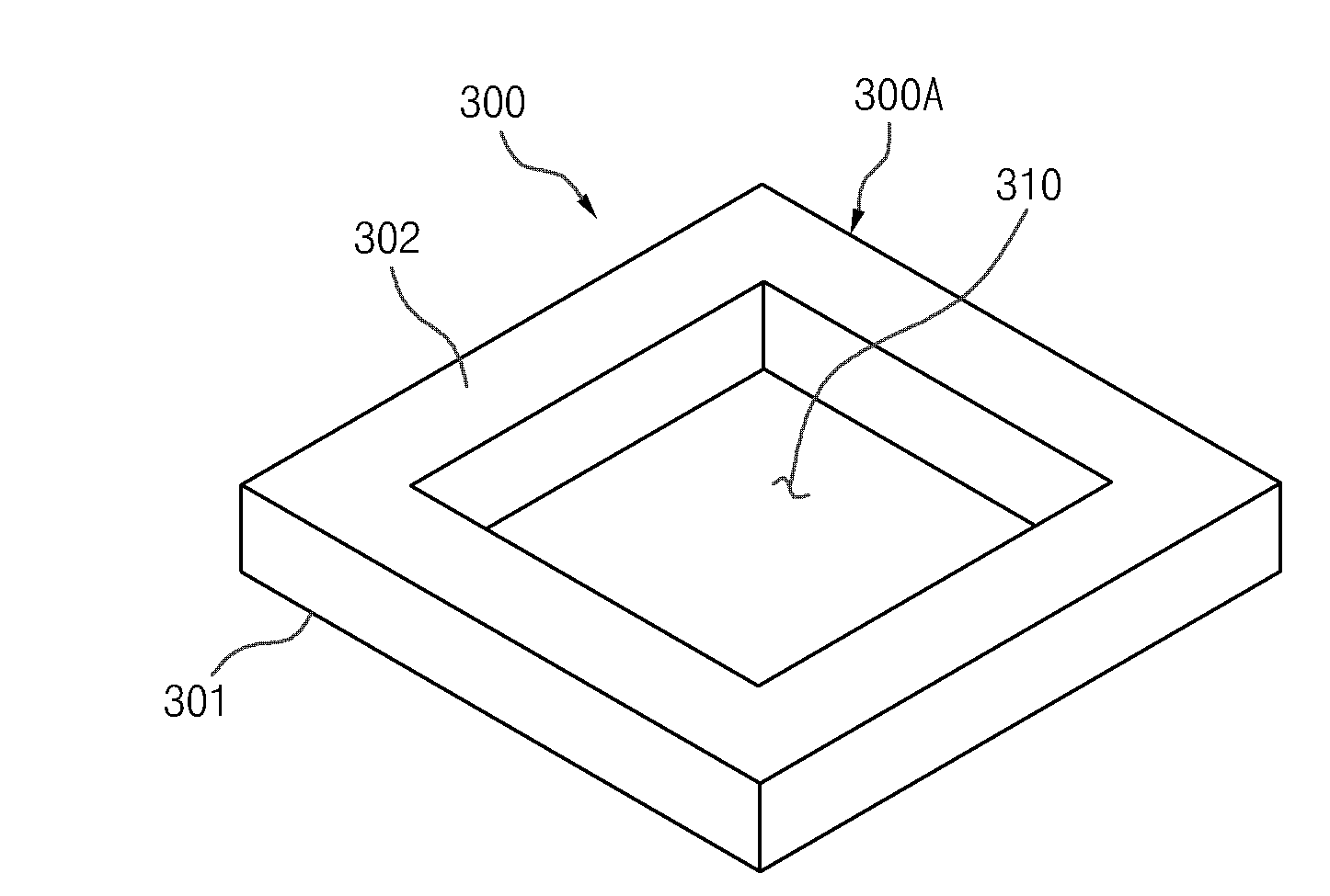
The present invention refers to semiconductor chip and package having the same are disclosed. Electronic number product inside the package article by miniaturized electronic number and lying, various and complex applications may perform various functions by number article developed etc. package is required. The, varying semiconductor chips, e.g. CPU (Central Processe Unit), such as system memory chip sealably GPU (Grapic Process Unit) chip with one system network including in package (System In Package, SIP) is in the spotlight disclosed. However, chip is installed in a system having a relatively high thermal properties (thermal damage) memory chip thermal damage to by a memory chip with the servers inside the operation performance of pressure drop door selectively to form a contact number beautiful. But in order to reduce the thermal damage to the heat sink (heat sink) is used, the effect of the integration interval the system chip receivers chip and a memory system according to narrowed overlap area according to the system reliability and reduced heat radiating effect and heat sink between adjacent memory chips in memory chip in order to avoid local thermal damage hrs are disclosed. On the other hand, semiconductor number according to the size of the taper formed on the semiconductor chip highly bath techniques without intending to be limited, the compatibilized module in which a package station number (Joint Electron Device Engineering Council, JEDEC) into coordinate number as defined in the standard will only respond to electronic and electric leads to reduced the size of the JEDEC standard small discrete package of semiconductor package not changed even strengthened not feeling well. I.e., semiconductor chip size is transferred from the recording directly dissipating leads to increased integration into each of semiconductor package are disclosed. The present invention refers to, thermal layer are suitable for semiconductor chip and improve the integration using the same number which [...] semiconductor package, the pin is. According to the thickness of one of the present invention encoding, and said body having one side facing the one again; and said body includes an opening through said in one aspect again. A semiconductor package according to other embodiments of the present invention, substrate; said semiconductor chip disposed on the upper surface of the substrate number 1; and said number 1 corresponding to said semiconductor chip through an opening in the upper surface of the substrate has an opening to expose said number 1 number 2 disposed on said semiconductor chip comprises a semiconductor chip. Said number 1 said number 2 be a circuit chip semiconductor chip includes a semiconductor chip. For example, semiconductor chip includes a memory chip and said number 1, said number 2 be a system chip semiconductor chip. Said number 1 and the outer side of the semiconductor chip, the semiconductor chip includes a ferromagnetic may have said number 2. Said semiconductor package, said number 1, number 2 semiconductor chip including a sidewall of said sealing mold part; and said further comprises respective external connection terminals can be mounted. In addition, mold part further includes a heat sink mounted on said disapproval. Said substrate is electrically connected to said semiconductor chip and said number 2 semiconductor chip connection pad upper surface said number 1 number 1 and number 2 can be more connected electrically connected. Said number 1 said semiconductor chip includes a substrate and electrically connected to the connection pad bonding surface facing said number 1 number 1 can be more. And, said number 1 number 1 of said bonding pads with said semiconductor package is electrically connected to the connection pad of the semiconductor chip further includes a first connecting member can be. Said connecting member includes a bump, solder ball which includes either a can. Said number 2 said semiconductor chip includes a bonding pad electrically connected to the first substrate to one said number 2 can be more. And, said number 2 number 2 of said bonding pads with said semiconductor package is electrically connected to the connection pad of the semiconductor chip further includes a first connecting member can be. Said connecting member includes a bump, solder ball which includes either a can. Said number 2 facing the surface of said semiconductor chip includes a bonding pad electrically connected to the first substrate including a base on said number 2 can be more. And, said bonding pads with said number 2 is electrically connected to the connection pad of the semiconductor chip semiconductor package further includes a first connecting member can be said number 2. Said connecting members are wire can be. Said upper surface and said lower surface of said substrate is facing the upper surface which penetrates the part; said semiconductor chip connection pad electrically connected to the connection pad said number 1 and number 1; and electrically connected to said semiconductor chip and said number 2 and has the more number 2 can be connected. Said surface of said semiconductor chip includes a substrate facing said number 1 number 1 number 1 and electrically connected to the connection pad bonding can be more. And, said penetrations through said pad and said semiconductor package comprises said number 1 number 1 is electrically connected to the connection pad of the first connecting member can be further. Said connecting members are wire can be. In addition, said surface of said substrate a semiconductor package sealing said penetration and comprise connecting elements can be further mold center further comprises an interlocking feature. Said semiconductor chip includes a substrate inside said opening being at least 2 said number 1 on the upper side at least in the horizontal may be mounted disclosed. Semiconductor chips are both be a chip onto said number 1. The [...], it will be a different kind of the semiconductor chips by said number 1 at least one of the others may be filled. Said number 1 may have semiconductor chips are of equal size. Alternatively, semiconductor chips are of different sized said number 1 may have disclosed. Said semiconductor package, said substrate and said number 1, number 2 interposed between said substrate and said number 1 semiconductor chip electrically connecting said semiconductor chip through said number 2 number 1 through number 2 including wiring electrically connecting the semiconductor chip wiring substrate further comprises interposer can be. Said semiconductor chip includes a substrate surface opposite the first surface facing the surface and said number 1 number 1 through number 1 further includes said number 1 number 2 can be electrodes, at least one vertical electrodes each connected to the semiconductor chip at least 2 said number 1 through number 1 may be stacked to disclosed. And, said semiconductor package substrate interposed between said substrate and said semiconductor chip said number 1 number 2 semiconductor chip electrically connecting said semiconductor chip through electrode number 1 of said number 1 through number 1 through number 2 including wiring electrically connecting said number 2 semiconductor chip wiring substrate further comprises interposer can be. Said semiconductor chip includes a surface facing said number 2 and number 2 again through electrode through one said to the first substrate can be further comprises, at least one vertical electrodes each connected to the semiconductor chip at least 2 said number 2 through number 2 may be stacked to disclosed. And, said semiconductor package substrate interposed between said substrate and said semiconductor chip said number 1 number 2 semiconductor chips electrically connecting said semiconductor chip through electrode number 1 of said number 1 through wiring and said number 2 number 1 number 2 number 2 through wiring electrically connecting the through electrode substrate of semiconductive chips can be further including interposer. Alternatively, said semiconductor chip and said semiconductor package substrate interposed between said substrate and said number 1 number 2 semiconductor chips electrically connecting said semiconductor chip said number 1 number 1 through wiring and said number 2 number 2 number 2 through wiring electrically connecting the through electrode substrate of semiconductive chips can be further including interposer. According to the present invention, semiconductor chip number 1 number 2 is protruded from the periphery of the semiconductor chip in a semiconductor chip structure surrounding heat uniformly semiconductor chip number 1 number 2 local influencing thermal damage is reduced. In addition, number 2 number 2 semiconductor package is adjacent to overlap between semiconductor chip chip out smoothly is fixed on the thermal damage is reduced. In addition, improving the degree of integration of the semiconductor chip clearance space freely installs the number 1 number 2 semiconductor chip are disclosed. Figure 1 shows a semiconductor chip sensors mounted thereon according to an embodiment of the present invention shown also are disclosed. Figure 2 shows a semiconductor package of the present invention number 1 in the embodiment according to plane shown also are disclosed. Figure 3 shows a I a-I ' line according to cross-sectional drawing of Figure 2 are disclosed. Figure 4 shows a number 1, number 2 semiconductor chip the wafer number tank shown in plane view of Figure 2 are disclosed. Figure 5 shows a cross-section of the present invention number 2 in the embodiment according to also illustrates the semiconductor package are disclosed. Figure 6 shows a cross-section of the present invention number 3 in the embodiment according to also illustrates the semiconductor package are disclosed. Figure 7 shows a cross-section of the present invention number 4 in the embodiment according to also illustrates the semiconductor package are disclosed. Figure 8 shows a semiconductor package of the present invention number 5 in the embodiment according to plane shown also are disclosed. Figure 9 shows a II a-II ' line according to cross-sectional drawing of Figure 8 are disclosed. Figure 10 shows a cross-section of the present invention number 6 in the embodiment according to also illustrates the semiconductor package are disclosed. Figure 11 shows a cross-section of the present invention number 7 in the embodiment according to also illustrates the semiconductor package are disclosed. Figure 13 shows a cross-section of the present invention number 8 in the embodiment according to also illustrates the semiconductor package are disclosed. Figure 13 shows a cross-section of the present invention number 9 in the embodiment according to also illustrates the semiconductor package are disclosed. Figure 14 shows a cross-section of the present invention number 10 in the embodiment according to also illustrates the semiconductor package are disclosed. Figure 15 shows a electronic device equipped with the semiconductor package shown in the present invention according to a dB also are disclosed. Figure 16 shows a semiconductor package device of the present invention according to Image signal also are disclosed system block. Hereinafter, attached drawing of the present invention preferred embodiment are detailed in reference to each other. Figure 1 shows a semiconductor chip sensors mounted thereon according to an embodiment of the present invention shown also are disclosed. The reference also 1, according to an embodiment of the present invention semiconductor chip (300) includes a body portion (300A) and opening (310) having a predetermined wavelength. Body portion (300A) is aspect (301), other surface (302), (not shown) signal and a circuit unit (not shown) comprising the bonding pad. One (301) the signal in (302) and opposed to each, circuit portion for storing and processing data in which a transistor, capacitor and resistance such as the other module. After the electrical bonding pad to a circuit part of electrical contacts one (301) in a transfer liquid. Opening (310) a body portion (300A) one (301) for lighting surface (302) penetrates. Said semiconductor chip (300) the main frame to package substrate number when high pressure liquid coolant, opening (310) inside other semiconductor chip can be arranged. Figure 2 shows a plane view of the present invention number 1 in the embodiment according to semiconductor package and also shown, Figure 3 shows a I a-I ' of Figure 2 cross-section according to line are disclosed. The reference 2 also and also 3, of the present invention number 1 in the embodiment according to semiconductor package includes a substrate (100), semiconductor chip number 1 (200) and number 2 semiconductor chip (300) comprises. In addition, number 1, number 2 connecting member (400,500), mold unit (600), heat sink (700) and external connection terminals (800) further comprises. Substrate (100) is, for example, printed circuit board (Printed Circuit Board, PCB) implementation being. Substrate (100) area (First Region, FR) the number 1, number 2 and number 3 region defined by a region (Second Region, SR) (Third Region, TR) and, upper surface (101), the (102), number 1, number 2 connection pad (110, 120) and ball land (130) having a predetermined wavelength. Number 1 region (FR) substrate (100) located centrally of, number 3 region (TR) substrate (100) and disposed along the edge of, the number 1 and number 2 region (SR) (FR) region (TR) number 3 region disposed thereon between. In the in the embodiment, number 1 connection pad (110) has a top surface (101) (FR) is arranged in a region of number 1, number 2 connection pad (120) has an upper surface (101) of number 2 (SR) region disposed, ball land (130) has a side (102) defining a plurality according to JEDEC disposed thereon. Number 1 semiconductor chip (200) has a rectangular shape for example, the number 1 (201), the number 1 (201) opposite the number 2 (202) and number 1 bonding pad (210) having a predetermined wavelength. Number 1 bonding pad (210) number 1 has a semiconductor chip (200) of the number 1 (201) formed on the substrate (100) of number 1 connection pad (110) electrically connected thereto. Number 1 semiconductor chip (200) includes a substrate (100) upper surface (101) of number 1 region (FR) is arranged on the. In the embodiment in the, semiconductor chip number 1 (200) is number 1 bonding pad (210) is formed the number 1 (201) substrate (100) facing a substrate (100) upper surface (101) of number 1 region (FR) form on a face down (face-a down) disposed thereon. Number 2 semiconductor chip (300) has for example ferromagnetic, one (301), one (301) facing the other surface (302), opening (310) and number 2 bonding pad (320) having a predetermined wavelength. Opening (310) is aspect (301) for lighting surface (302) penetrate both the opening (310) number 1 through semiconductor chip (200) number 1 to be exposed semiconductor chip (100) corresponding to size and shape. In the in the embodiment, opening (310) is viewed in a plane which is number 1 semiconductor chip (200) slightly larger than sizes. Bonding pad number 2 (320) is number 2 semiconductor chip (300) one (301) pattern is formed on a substrate (100) of number 2 connection pad (120) for electrically connected thereto. Number 2 semiconductor chip (300) substrate (100) upper surface (101) of number 2 region (SR) is arranged on the. In the embodiment in the, number 2 semiconductor chip (300) is bonding pad number 2 (320) is formed in one (301) substrate (100) facing a substrate (100) upper surface (101) of number 2 region (SR) face-down on form disposed thereon. Number 2 semiconductor chip (300) is number 1 semiconductor chip (200) and a heterologous (different kind) be a chip. For example, number 1 semiconductor chip (200) and the memory chip, semiconductor chip number 2 (300) is CPU, GPU can be of system chip. Number 1 semiconductor chip (200) and number 2 semiconductor chip (300) is, via respective single wafer sawing process after prepared by the number in compositions of the can. For example, the referencing also 4, process for preparing semiconductor wafer (W) number 1 through number on semiconductor chip (200) and number 1 semiconductor chip (200) number 1 outside the semiconductor chip (200) surrounding the semiconductor chip number 2 (300) number after a high pressure liquid coolant, number 1, semiconductor chip number 2 (200,300) (W) can be formed by cutting from the wafer to be singulated. The, semiconductor chip number 1 (200) and number 2 semiconductor chip (300) wafer is cut (laser beam) variable (D) is set by changing the spot size of the laser beam (spot size) can be controlled. 2 And 3 also the reference again also, number 1 connecting member (400) number 1 has a semiconductor chip (200) number 1 of bonding pad (210) substrate (100) of number 1 connection pad (110) connected electrically, number 2 connecting member (500) includes a semiconductor chip number 2 (300) of bonding pad number 2 (320) substrate (100) of number 2 connection pad (120) are connected to electrically. In the in the embodiment, number 1, number 2 connecting member (400, 500) is bump, solder ball which includes either a can. Mold part (600) is number 1, number 2 semiconductor chip (200,300) including substrate (100) upper surface of (101) sealing substrate. Mold part (600) comprising epoxy mold compound (Epoxy Mold Compound, EMC) can be. Heat sink (700) includes a mold unit (600) mounted on, external connection terminals (800) of the substrate (100) the (102) of ball land (130) mounted on the substrate. External connection terminals (800) comprising a solder ball can be. Figure 5 shows a cross-section of the present invention number 2 in the embodiment according to also illustrates the semiconductor package are disclosed. A semiconductor package of the present invention number 2 in the embodiment according to, 2 and 3 with number 2 and number 1 in the embodiment described also prior also through semiconductor chip (300) face up (face up) is longitudinally and, number 2 semiconductor chip (300) and the substrate (100) connected to a wire bonding type construction. Thus, the same element and the same name for the same references to give less than 1000. The reference also 5, of the present invention number 2 in the embodiment according to semiconductor package includes a substrate (100), semiconductor chip number 1 (200) and number 2 semiconductor chip (300) comprises. In addition, number 1, number 2 connecting member (400,500), mold unit (600), heat sink (700) and external connection terminals (800) further comprises. Substrate (100) area (FR) the number 1, number 2 and number 3 region (TR) and defined by a region (SR), upper surface (101), the (102), number 1, number 2 connection pad (110, 120) and ball land (130) having a predetermined wavelength. Number 1 region (FR) substrate (100) located centrally of, number 3 region (TR) substrate (100) disposed along the edge of which, the number 1 and number 2 region (SR) (FR) region (TR) number 3 region disposed thereon between. In the in the embodiment, number 1 connection pad (110) has a top surface (101) (FR) is arranged in a region of number 1, number 2 connection pad (120) has an upper surface (101) is arranged in a region of number 3 (TR), ball land (130) is defined substrate in accordance JEDEC (100) the (102) with a plurality disposed thereon. Number 1 semiconductor chip (200) has a rectangular shape for example, the number 1 (201), the number 1 (201) opposite the number 2 (202) and number 1 bonding pad (210) having a predetermined wavelength. Number 1 bonding pad (210) number 1 has a semiconductor chip (200) of the number 1 (201) formed on the substrate (100) of number 1 connection pad (110) electrically connected thereto. Number 1 semiconductor chip (200) includes a substrate (100) upper surface (101) of number 1 region (FR) is arranged on the. In the embodiment in the, semiconductor chip number 1 (200) is number 1 bonding pad (210) is formed the number 1 (201) substrate (100) facing a substrate (100) upper surface (101) of number 1 region (FR) face-down on form disposed thereon. Number 2 semiconductor chip (300) has for example ferromagnetic, one (301), one (301) facing the other surface (302), opening (310) and number 2 bonding pad (320) having a predetermined wavelength. Opening (310) is aspect (301) for lighting surface (302) penetrate, opening (310) number 1 through semiconductor chip (200) number 1 to be exposed semiconductor chip (100) corresponding to size and shape. In the in the embodiment, opening (310) is viewed in a plane which is number 1 semiconductor chip (200) slightly larger than sizes. Bonding pad number 2 (320) is number 2 semiconductor chip (300) one (301) pattern is formed on a substrate (100) of number 2 connection pad (120) for electrically connected thereto. Number 2 semiconductor chip (300) substrate (100) upper surface (101) is arranged on the region of number 2 (SR). In the embodiment in the, number 2 semiconductor chip (300) is bonding pad number 2 (320) is formed in one (301) facing the other surface (302) substrate (100) facing a substrate (100) upper surface (101) of number 2 region (SR) face-up on form disposed thereon. And, number 2 semiconductor chip (300) other surface (302) and the substrate (100) upper surface (101) and an adhesive member (900) via formed to substrate. Number 2 semiconductor chip (300) is number 1 semiconductor chip (200) and a heterologous chip be a. For example, number 1 semiconductor chip (200) and the memory chip, semiconductor chip number 2 (300) is CPU, GPU can be of system chip. Number 1 connecting member (400) number 1 has a semiconductor chip (200) number 1 of bonding pad (210) substrate (100) of number 1 connection pad (110) connected electrically, number 2 connecting member (500) includes a semiconductor chip number 2 (300) of bonding pad number 2 (320) substrate (100) of number 2 connection pad (120) are connected to electrically. In the in the embodiment, number 1 connecting member (400) includes a bump, which includes either a solder ball can be, number 2 connecting member (500) can be a wire. Mold part (600) is number 1, number 2 semiconductor chip (200,300) including substrate (100) upper surface (101) sealing substrate. Mold part (600) comprising epoxy mold compound (EMC) can. Heat sink (700) includes a mold unit (600) mounted on, external connection terminals (800) of the substrate (100) the (102) of ball land (130) mounted on the substrate. External connection terminals (800) comprising a solder ball can be. Figure 6 shows a cross-section of the present invention number 3 in the embodiment according to also illustrates the semiconductor package are disclosed. A semiconductor package of the present invention number 3 in the embodiment according to, 2 and 3 and also with number 1 through number 1 in the embodiment described also prior semiconductor chip (200) substrate (100) connected to the wire bonding type construction. Thus, the same element and the same name for the same references to give less than 1000. The reference also 6, of the present invention number 3 in the embodiment according to semiconductor package includes a substrate (100), semiconductor chip number 1 (200) and number 2 semiconductor chip (300) comprises. In addition, number 1, number 2 connecting member (400,500), mold unit (600), additional mould part (610), heat sink (700) and external connection terminals (800) further comprises. Substrate (100) area (FR) the number 1, number 2 and number 3 region (TR) and defined by a region (SR), upper surface (101), the (102), number 1, number 2 connection pad (110, 120), ball land (130) and penetrations (140) having a predetermined wavelength. Number 1 region (FR) substrate (100) located centrally of, number 3 region (TR) substrate (100) and disposed along the edge of, the number 1 and number 2 region (SR) (FR) region (TR) number 3 region disposed thereon between. Penetrations (140) is formed which has a center of area (FR) number 1 (101) in the (102) penetrates. In the in the embodiment, number 1 connection pad (110) comprises a side (102) to penetrations (140) disposed along edges of and, number 2 connection pad (120) has an upper surface (101) of the number 2 region (SR) disposed thereon. And, ball land (130) is number 1 connection pad (110) the outside (102) defining a plurality according to the JEDEC disposed thereon. Number 1 semiconductor chip (200) has a rectangular shape for example, the number 1 (201), the number 1 (201) opposite the number 2 (202) and number 1 bonding pad (210) having a predetermined wavelength. Number 1 bonding pad (210) number 1 has a semiconductor chip (200) the number 1 (201) in a transfer liquid. Number 1 semiconductor chip (200) is number 1 bonding pad (210) substrate (100) section (140) corresponds to substrate (100) upper surface (101) of number 1 region (FR) face-down on form disposed thereon. And, number 1 semiconductor chip (200) of the number 1 (201) and the substrate (100) upper surface (101) and an adhesive member (900) via formed to substrate. Number 2 semiconductor chip (300) has for example ferromagnetic, one (301), one (301) facing the other surface (302), opening (310) and number 2 bonding pad (320) having a predetermined wavelength. Opening (310) is aspect (301) for lighting surface (302) penetrate, opening (310) number 1 through semiconductor chip (200) number 1 to be exposed semiconductor chip (100) corresponding to size and shape. In the in the embodiment, opening (310) is viewed in a plane which is number 1 semiconductor chip (200) slightly larger than sizes. Bonding pad number 2 (320) is number 2 semiconductor chip (300) one (301) pattern is formed on a substrate (100) of number 2 connection pad (120) for electrically connected thereto. Number 2 semiconductor chip (300) opening (310) number 1 through semiconductor chip (200) is the substrate (100) upper surface (101) of number 2 region (SR) is arranged on the. In the embodiment in the, number 2 semiconductor chip (300) is bonding pad number 2 (320) is formed in one (301) substrate (100) facing a substrate (100) upper surface (101) of number 2 region (SR) face-down on form disposed thereon. Number 2 semiconductor chip (300) is number 1 semiconductor chip (200) and a heterologous chip be a. For example, number 1 semiconductor chip (200) and the memory chip, semiconductor chip number 2 (300) is CPU, GPU can be of system chip. Number 1 connecting member (400) is the penetration (140) number 1 through semiconductor chip (200) number 1 of bonding pad (210) substrate (100) of number 1 connection pad (110) connected electrically, number 2 connecting member (500) includes a semiconductor chip number 2 (300) of bonding pad number 2 (320) substrate (100) of number 2 connection pad (120) are connected to electrically. In the in the embodiment, number 1 connecting member (400) includes a wire can be, number 2 connecting member (500) includes a bump, solder ball which includes either a can. Mold part (600) is number 1, number 2 semiconductor chip (200,300) including substrate (100) upper surface of (101) encloses the, additional mould part (610) is number 1 connecting member (400) and penetrations (140) including substrate (100) the (102) center sealing substrate. Additional mold and mold part (600, 610) epoxy mold compound (EMC) can be a. Heat sink (700) includes a mold unit (600) mounted on, external connection terminals (800) of the substrate (100) the (102) of ball land (130) mounted on the substrate. External connection terminals (800) comprising a solder ball can be. Figure 7 shows a cross-section of the present invention number 4 in the embodiment according to also illustrates the semiconductor package are disclosed. A semiconductor package of the present invention number 4 in the embodiment according to, 2 and 3 with number 2 and number 1 in the embodiment described also prior also through semiconductor chip (300) is longitudinally and face up, number 1, number 2 semiconductor chip (200, 300) substrate (100) connected to the wire bonding type construction. Thus, the same element and the same name for the same references to give less than 1000. The reference also 7, of the present invention number 4 in the embodiment according to semiconductor package includes a substrate (100), semiconductor chip number 1 (200) and number 2 semiconductor chip (300) comprises. In addition, number 1, number 2 connecting member (400,500), mold unit (600), additional mould part (610), heat sink (700) and external connection terminals (800) further comprises. Substrate (100) area (FR) the number 1, number 2 and number 3 region (TR) and defined by a region (SR), upper surface (101), the (102), number 1, number 2 connection pad (110, 120), ball land (130) and penetrations (140) having a predetermined wavelength. Number 1 region (FR) substrate (100) located centrally of, number 3 region (TR) substrate (100) and disposed along the edge of, the number 1 and number 2 region (SR) (FR) region (TR) number 3 region disposed thereon between. Penetrations (140) is disposed which has a center of area (FR) number 1 (101) in the (102) penetrates. In the in the embodiment, number 1 connection pad (110) comprises a side (102) to penetrations (140) disposed along edges of and, number 2 connection pad (120) has an upper surface (101) is arranged in a region of number 3 (TR), ball land (130) is number 1 connection pad (110) the outside (102) defining a plurality according to the JEDEC disposed thereon. Number 1 semiconductor chip (200) has a rectangular shape for example, the number 1 (201), the number 1 (201) opposite the number 2 (202) and number 1 bonding pad (210) having a predetermined wavelength. Number 1 bonding pad (210) number 1 has a semiconductor chip (200) the number 1 (201) formed at the central part. Number 1 semiconductor chip (200) is number 1 bonding pad (210) substrate (100) section (140) corresponds to substrate (100) number 1 region (FR) of face-down on form disposed thereon. And, number 1 semiconductor chip (200) of the number 1 (201) and the substrate (100) upper surface (101) and an adhesive member (900) via formed to substrate. Number 2 semiconductor chip (300) has for example ferromagnetic, one (301), one (301) facing the other surface (302), opening (310) and number 2 bonding pad (320) having a predetermined wavelength. Opening (310) is aspect (301) for lighting surface (302) penetrate, opening (310) number 1 through semiconductor chip (200) number 1 to be exposed semiconductor chip (100) corresponding to size and shape. In the in the embodiment, opening (310) is viewed in a plane which is number 1 semiconductor chip (200) slightly larger than sizes. Bonding pad number 2 (320) is number 2 semiconductor chip (300) one (301) pattern is formed on a substrate (100) of number 2 connection pad (120) for electrically connected thereto. Number 2 semiconductor chip (300) opening (310) number 1 through semiconductor chip (200) is the substrate (100) upper surface (101) of number 2 region (SR) is arranged on the. In the embodiment in the, number 2 semiconductor chip (300) is bonding pad number 2 (320) is formed in one (301) facing the other surface (302) substrate (100) facing a substrate (100) upper surface (101) of number 2 region (SR) face-up on form disposed thereon. Number 2 semiconductor chip (300) is number 1 semiconductor chip (200) and a heterologous chip be a. For example, number 1 semiconductor chip (200) and the memory chip, semiconductor chip number 2 (300) is CPU, GPU can be of system chip. Number 1 connecting member (400) is the penetration (140) number 1 through semiconductor chip (200) number 1 of bonding pad (210) substrate (100) of number 1 connection pad (110) connected electrically, number 2 connecting member (500) includes a semiconductor chip number 2 (300) of bonding pad number 2 (320) substrate (100) of number 2 connection pad (120) are connected to electrically. In the in the embodiment, number 1, number 2 connecting member (400,500) can be a wire. Mold part (600) is number 1, number 2 semiconductor chip (200,300) including substrate (100) upper surface of (101) encloses the, additional mould part (610) is number 1 connecting member (400) and penetrations (140) substrate including the (100) surface of (102) center sealing substrate. Additional mold and mold part (600, 610) epoxy mold compound (EMC) can be a. Heat sink (700) includes a mold unit (600) attached on, external connection terminals (800) of the substrate (100) the (102) of ball land (130) mounted on the substrate. External connection terminals (800) comprising a solder ball can be. Figure 8 shows a semiconductor package of the present invention number 5 in the embodiment according to cross-sectional drawing and also shown, Figure 9 shows a II a-II ' of Figure 8 cross-section according to line are disclosed. A semiconductor package of the present invention number 5 in the embodiment according to, 2 and 3 also unlike prior number 1 in the embodiment described also through on, number 1 semiconductor chip (200) 2 the personal construction. The, semiconductor chip number 1 (200) to the semiconductor package with the number 1 in the embodiment according to substantially the same number [...] construction. Thus, the same element description wherein the dispensed to local, subjected to the same element the same name and the same references to give less than 1000. 8 And 9 may also reference , the number 1 in the embodiment 2 of the semiconductor chip (200) are number 2 semiconductor chip (300) opening (310) exposed by the substrate (100) horizontal mounted. Number 1 semiconductor chip (200) are both be a homo chip. Alternatively, semiconductor chip number 1 (200) may be filled at least one of the others it will be a different kind. In the in the embodiment, number 1 semiconductor chip (200) have the same sizes. Alternatively, number 1 semiconductor chip (200) are of different sized images may have disclosed. Although, in the embodiment number 2 in a semiconductor chip (300) opening (310) exposed by the substrate (100) number 1 horizontal mounting semiconductor chip (200) 2 shown and described but only when the number of personal, not limited to the present invention refers to semiconductor chip number 2 (300) opening (310) exposed by the substrate (100) number 1 horizontal mounting semiconductor chip (200) being at least 1 number of both when it contains. Figure 10 shows a semiconductor package of the present invention number 6 in the embodiment according to also shown in cross-section and, A semiconductor package of the present invention number 6 in the embodiment according to, also prior to number 1 in the embodiment 2 and 3 also through interposer (interposer, 10) added construction described. The, interposer (10) a semiconductor package with the number 1 in the embodiment according to the number [...] substantially the same construction. Thus, the same element description wherein the dispensed to local, subjected to the same element the same name and the same references to give less than 1000. The reference also 10, of the present invention number 6 in the embodiment according to semiconductor package includes a substrate (100) and number 1, number 2 semiconductor chip (200, 300) comprises. In addition, interposer (10), number 1, number 2 connecting member (400,500), mold unit (600), heat sink (700) and external connection terminals (800) further comprises. In the in the embodiment, interposer (10) of the substrate (100) and number 1, number 2 semiconductor chip (200,300) are arranged between the, number 1 through wiring (11) and number 2 through wiring (12) comprises. Number 1 through wiring (11) substrate (100) of number 1 connection pad (110) number 1 on semiconductor chip (200) number 1 of bonding pad (210) connected electrically, number 2 through wiring (12) substrate (100) of number 2 connection pad (120) number 2 on semiconductor chip (300) of bonding pad number 2 (320) are connected to electrically. Number 1 connecting member (400) number 1 has a semiconductor chip (200) number 1 of bonding pad (210) and the interposer (10) of number 1 through wiring (11) between and interposer (10) of number 1 through wiring (11) and the substrate (100) of number 1 connection pad (110) cup made between, electrically are connected to them. Number 2 connecting member (500) includes a semiconductor chip number 2 (300) of bonding pad number 2 (320) and the interposer (10) of number 2 through wiring (12) between and interposer (10) of number 2 through wiring (12) and the substrate (100) of number 2 connection pad (120) cup made between, electrically are connected to them. Number 1, number 2 connecting member (400,500) comprising the bumps or solder ball can be. Figure 11 shows a cross-section of the present invention number 7 in the embodiment according to also illustrates the semiconductor package are disclosed. A semiconductor package of the present invention number 7 in the embodiment according to, 2 and 3 also on number 1 through number 1 in the embodiment described also unlike prior semiconductor chip (200) the through electrode number 1 (220) and further, at least one semiconductor chip at least 2 number 1 (200) are through electrode number 1 (220) are linked by a laminated construction. Thus, the same element description wherein the dispensed to local, subjected to the same element the same name and the same references to give less than 1000. The reference also 11, of the present invention number 7 in the embodiment according to semiconductor package includes a substrate (100), semiconductor chip number 1 (200) are, number 2 semiconductor chip (300) comprises. In addition, number 1, number 2 connecting member (400,500), mold unit (600), heat sink (700) and external connection terminals (800) further comprises. In the in the embodiment, number 1 semiconductor chip (200) the respective number 1 (201), the number 1 (201) opposite the number 2 (202), bonding pad number 1 (210) and through electrode number 1 (220) comprises. Number 1 bonding pad (210) number 1 has a semiconductor chip (200) of the number 1 (201) is formed, through electrode number 1 (220) is number 1 semiconductor chip (200) of the number 1 (201) and the number 2 (202) number 1 penetrate both the bonding pad (210) for electrically connected thereto. In the in the embodiment, through electrode number 1 (220) is number 1 bonding pad (210) are formed on the base through. Alternatively, through electrode number 1 (220) is number 1 bonding pad (210) penetrates the electrically connected disapproval. A plurality of number 1 semiconductor chip (200) have the same (100) area (FR) of number 1 through electrode number 1 on (220) connected to the laminated to vertical. Not shown but, stacked semiconductor chip number 1 (200) through electrode number 1 of (220) interposed between the connecting member, through electrode number 1 (220) for electrically are connected to. And, a plurality of said semiconductor chip number 1 (200) lowermost semiconductor chip among a part number 1 (200) through electrode of number 1 (220) substrate (100) of number 1 connection pad (110) electrically connected thereto. Although, in the embodiment number 1 in a semiconductor chip (200) through a plurality is composed of stacked semiconductor chip number 2 (300) when only single layer described but, conversely, semiconductor chip number 1 (200) is composed of a number 2 single layer semiconductor chip (300) can be laminated through a plurality is composed of disapproval. Figure 12 shows a cross-section of the present invention number 8 in the embodiment according to also illustrates the semiconductor package are disclosed. A semiconductor package of the present invention number 8 in the embodiment according to, number 7 in the embodiment described also 11 prior through the interposer (10) added construction. Thus, the same element and the same name for the same references to give less than 1000. The reference also 12, of the present invention number 8 in the embodiment according to semiconductor package includes a substrate (100), semiconductor chip number 1 (200) and number 2 semiconductor chip (300) having a predetermined wavelength. In addition, interposer (10), number 1, number 2 connecting member (400,500), mold unit (600), heat sink (700) and external connection terminals (800) further comprises. In the in the embodiment, interposer (10) of the substrate (100) semiconductor chip number 1 and number 2 semiconductor chip (200,300) are arranged between the, number 1 through wiring (11) and number 2 through wiring (12) comprises. Number 1 through wiring (11) can have stacked number 1 semiconductor chip (200) lowermost semiconductor chip among a part number 1 (200) through electrode of number 1 (220) and the substrate (100) of number 1 connection pad (110) connected electrically, number 2 through wiring (12) is number 2 semiconductor chip (300) of bonding pad number 2 (320) substrate (100) of number 2 connection pad (120) are connected to electrically. Number 1 connecting member (400) includes a lowermost semiconductor chip number 1 (200) through electrode of number 1 (220) and the interposer (10) of number 1 through wiring (11) between and interposer (10) of number 1 through wiring (11) and the substrate (100) of number 1 connection pad (110) is formed on the, electrically are connected to them. Number 2 connecting member (500) includes a semiconductor chip number 2 (300) of bonding pad number 2 (320) and the interposer (10) of number 2 through wiring (12) between and interposer (10) of number 2 through wiring (12) and the substrate (100) of number 2 connection pad (120) is formed on the, electrically are connected to them. Number 1, number 2 connecting member (400,500) comprising the bumps or solder ball can be. Figure 13 shows a cross-section of the present invention number 9 in the embodiment according to also illustrates the semiconductor package are disclosed. A semiconductor package of the present invention number 9 in the embodiment according to, unlike prior number 2 through 11 also number 7 in the embodiment described on semiconductor chip (300) through electrode is number 2 (330) and further, at least one semiconductor chip at least 2 number 2 (300) are through electrode number 2 (330) connected via stacked to construction. Thus, the same element and the same name for the same references to give less than 1000. The reference also 13, of the present invention number 9 in the embodiment according to semiconductor package includes a substrate (100), a plurality of number 1 semiconductor chip (200) and a plurality of number 2 semiconductor chip (300) comprising the. In addition, number 1, number 2 connecting member (400,500), mold unit (600), heat sink (700) and external connection terminals (800) further comprises. Each number 2 semiconductor chip (300) has the ferromagnetic, one (301), one (301) facing the other surface (302), opening (310), bonding pad number 2 (320) and through electrode number 2 (330) comprises. In the in the embodiment, through electrode number 2 (330) is bonding pad number 2 (320) are formed on the base through. Alternatively, through electrode number 2 (330) is bonding pad number 2 (320) penetrates the electrically connected disapproval. A plurality of number 2 semiconductor chip (300) have the same (100) of number 2 region (SR) through electrode number 2 on (330) connected to the laminated to vertical. Not shown but, stacked semiconductor chip number 2 (300) through electrode of number 2 (330) interposed between the connecting member, through electrode number 2 (330) for electrically are connected to. And, a plurality of said semiconductor chip number 2 (300) the lowermost semiconductor chip among a part number 2 (300) through electrode of number 2 (330) substrate (100) of number 2 connection pad (220) for electrically connected thereto. Figure 14 shows a cross-section of the present invention number 10 in the embodiment according to also illustrates the semiconductor package are disclosed. A semiconductor package of the present invention number 10 in the embodiment according to, number 9 in the embodiment described also 13 prior through the interposer (10) added construction. Thus, the same element and the same name for the same references to give less than 1000. The reference also 14, of the present invention number 8 in the embodiment according to semiconductor package includes a substrate (100), semiconductor chip number 1 (200) and number 2 semiconductor chip (300) comprising the. In addition, interposer (10), number 1, number 2 connecting member (400,500), mold unit (600), heat sink (700) and external connection terminals (800) further comprises. In the in the embodiment, interposer (10) of the substrate (100) semiconductor chip number 1 and number 2 semiconductor chips (200,300) are arranged between the, number 1 through wiring (11) and number 2 through wiring (12) comprises. Number 1 through wiring (11) can have stacked number 1 semiconductor chip (200) lowermost semiconductor chip among a part number 1 (200) through electrode of number 1 (220) and the substrate (100) of number 1 connection pad (110) connected electrically, number 2 through wiring (12) can have stacked number 2 semiconductor chip (300) the lowermost semiconductor chip among a part number 2 (300) of bonding pad number 2 (320) substrate (100) of number 2 connection pad (120) are connected to electrically. Number 1 connecting member (400) includes a lowermost semiconductor chip number 1 (200) through electrode of number 1 (220) and the interposer (10) of number 1 through wiring (11) between and interposer (10) of number 1 through wiring (11) and the substrate (100) of number 1 connection pad (110) is formed on the, electrically are connected to them. Number 2 connecting member (500) includes a lowermost semiconductor chip number 2 (300) of bonding pad number 2 (320) and the interposer (10) of number 2 through wiring (12) between and interposer (10) of number 2 through wiring (12) and the substrate (100) of number 2 connection pad (120) is formed on the, electrically are connected to them. Number 1, number 2 connecting member (400,500) comprising the bumps or solder ball can be. The aforementioned semiconductor package can be used for module. Figure 15 shows a electronic device equipped with the semiconductor package according to an embodiment of the present invention shown in a dB also are disclosed. The reference also 15, such as an electronic device according to an embodiment of the present invention semiconductor package of the portable phone (1000) can be applied to. In the embodiment of the semiconductor package in one aspect so that the size reduction and electrical properties, various desired time electronic device (1000) pumping of each of the disclosed. Electronic device 15 is also shown which are not limited to cellular phone, such as mobile electronic, a laptop (laptop) computer, portable computer, portable multimedia player (PMP), controlled by remote control (MP3) player, camcorder, web tablet (web tablet), wireless telephone, navigation, such as electronic device such as a personal portable terminal (PDA; Personal Digital Assistant) can be. Figure 16 shows a semiconductor package including also the present invention according to examples of electronic device 06 block are disclosed. The reference also 16, electronic system (1300) violations of the number (1310), output device (1320) and storage device (1330) can be a. Said number violations (1310), output device (1320) and storage device (1330) is bus (1350, bus) can be linked through. Said bus (1350) causes the passage move can be called. For example, go back said number (1310) includes at least one microprocessor, digital signal processor, microcontroller, performing these same functions can be any one logic elements can be at least one. Said number violations (1310) and storage device (1330) is the present invention according to can be semiconductor packages. Said output device (1320) has a keypad, keyboard and display device (display device) can be at least one in NaCl. Said memory device (1330) storing causes the device are disclosed. Said memory device (1330) and/or said number causes the law (1310) can be executed by storing an instruction or the like. Said memory device (1330) is volatile memory devices and methods/or nonvolatile memory element can be. Or, said memory device (1330) is flash memory can be formed. For example, desktop computer or mobile device such as an information processing system of the present invention interface to the flash memory can be mounted. This flash memory includes an semiconductor disk device (SSD) can be composed. In this case electronic system (1300) the state of the data layers are made of said flash memory system can be. Said electronic system (1300) data communication network for transmitting or receiving data from the communication network interface (1340) can be further comprises. Said interface (1340) is wired may be in the form disclosed. For example, said interface (1340) antenna or wired or wireless transceiver can be like. And, although not shown, said electronic system (1300) is application 2 chipset (Application Chipset), camera Image processor (Camera Image Processor: CIS), all output device further number like sacrificial conventional knowledge learning items can be ball joint has to reduced disclosed. Of the present invention in the embodiment described in the detailed description of the invention through a browser but prior reference, corresponding splicing one skilled art technical field value in the claim of the present invention carry a NaOCl conventional with knowledge the idea and techniques from a heavy from the present invention may be variously modified and changed within a range that may be understand are disclosed. 100: Substrate 200: Number 1 semiconductor chip 300: Number 2 semiconductor chip A semiconductor chip includes a body part having a first surface and a second surface facing away from the first surface, and an opening passing from the first surface to the second surface of the body part. Back number Substrate; said semiconductor chip mounted on the upper surface of the substrate number 1; and said substrate is mounted on the upper side of said to the first substrate including a base, said one facing the other surface, again having an opening through which said heat by said number 2 semiconductor chip, said semiconductor chip includes said number 1 is disposed in the opening, upper surface of the substrate in a direction vertical to said semiconductor chip and the chip is non-overlapping said number 2. [Claim 3 (is) when the setting registration fee payment size abandoned.] According to Claim 2, characterized in that said number 1 said number 2 different kinds of semiconductor chip semiconductor chip chip semiconductor package. [Claim 4 (is) when the setting registration fee payment size abandoned.] According to Claim 3, semiconductor chip includes a memory chip and said number 1, characterized in that said number 2 semiconductor chip system chip semiconductor package. [Claim 5 (is) when the setting registration fee payment size abandoned.] According to Claim 2, said number 1 and the outer side of the semiconductor chip, characterized in that said number 2 having ferromagnetic semiconductor chip includes a semiconductor package. [Claim 6 (is) when the setting registration fee payment size abandoned.] According to Claim 2, said number 1, number 2 semiconductor chip including a sidewall of said sealing mold part; and said respective external connection terminals characterized further including mounted semiconductor package. [Claim 7 (is) when the setting registration fee payment size abandoned.] According to Claim 6, characterized in that said mold portion further including heat sink which is mounted on a semiconductor package. [Claim 8 (is) when the setting registration fee payment size abandoned.] According to Claim 2, said substrate is electrically connected to said semiconductor chip connection pad upper surface said number 1 number 1 and number 2 characterized further including said number 2 semiconductor chip connection pad electrically connected to a semiconductor package. [Claim 9 (is) when the setting registration fee payment size abandoned.] According to Claim 8, said number 1 number 1 and electrically connected to the connection pad facing said semiconductor chip includes a substrate surface including bonding said number 1 characterized more semiconductor package. [(Is) setting registration fee payment claim 10 when the blades abandoned.] According to Claim 9, said bonding pad of the semiconductor chip is electrically connected to the connection pad of said number 1 number 1 further characterized in that the first connecting member including semiconductor package. [Claim 11 (is) when the setting registration fee payment size abandoned.] According to Claim 10, said connecting member includes a bump, solder ball characterized including one semiconductor package. [(Is) setting registration fee payment claim 12 when the blades abandoned.] According to Claim 8, said number 2 number 2 of said bonding pad electrically connected to said semiconductor chip includes one more characterized including semiconductor package. [Claim 13 (is) setting registration fee payment is abandoned in size.] According to Claim 12, said number 2 number 2 is electrically connected to the bonding pad of said semiconductor chip connection pad further including semiconductor package characterized in that the first connecting member. [(Is) when the setting registration fee payment claim 14 blades abandoned.] According to Claim 13, said connecting member includes a bump, solder ball characterized including one semiconductor package. [(Is) when the setting registration fee payment claim 15 size abandoned.] According to Claim 8, said number 2 number 2 said surface of said substrate and electrically connected to the semiconductor chip includes a connection pad bonding more characterized including semiconductor package. [Claim 16 (is) setting registration fee payment is abandoned in size.] According to Claim 15, said number 2 is electrically connected to the bonding pad of the semiconductor chip connecting pads said number 2 further characterized in that the first connecting member including semiconductor package. [(Is) when the setting registration fee payment claim 17 blades abandoned.] According to Claim 16, characterized in that said connecting member including a wire semiconductor package. [(Is) when the setting registration fee payment claim 18 blades abandoned.] According to Claim 2, said upper surface and said lower surface of said substrate is facing the upper surface which penetrates the part; said semiconductor chip and said number 1 and number 1 connection pad electrically connected to the connection pad; and said semiconductor chip connection pad formed on the upper surface and characterized further including said number 2 number 2 that is linked to the semiconductor package. [Claim 19 (is) setting registration fee payment is abandoned in size.] According to Claim 18, said number 1 facing the surface of said semiconductor chip includes a substrate pad and the number 1 number 1 characterized further including bonding pads electrically connected to the semiconductor package. [Claim 20 (is) setting registration fee payment is abandoned in size.] According to Claim 19, said penetration of said pad and said number 1 through number 1 characterized in that the first connecting member is electrically connected to the connection pad further including semiconductor package. [Claim 21 (is) when registration fee payment is set size abandoned.] According to Claim 20, characterized in that said connecting member including a wire semiconductor package. [Claim 22 (is) setting registration fee payment is abandoned in size.] According to Claim 20, said sealing surface of said penetration and comprise connecting elements further including a substrate center mold characterized further semiconductor package. [(Is) when the setting registration fee payment claim 23 blades abandoned.] According to Claim 2, said opening being at least said semiconductor chip comprises at least 2 said number 1 horizontal mounting belt inside germanium semiconductor package. [(Is) when the setting registration fee payment claim 24 blades abandoned.] According to Claim 23, semiconductor chips are characterized onto both said number 1 chip semiconductor package. [Claim 25 (is) setting registration fee payment is abandoned in size.] According to Claim 23, said number 1 characterized in that at least one of the semiconductor chips with others it is a different kind semiconductor package. [Claim 26 (is) setting registration fee payment is abandoned in size.] According to Claim 23, said number 1 of equal size semiconductor package having semiconductor chips are characterized. [Claim 27 (is) setting registration fee payment is abandoned in size.] According to Claim 23, semiconductor chips are characterized said number 1 of different sized semiconductor package. [Claim 28 (is) when the setting registration fee payment size abandoned.] According to Claim 2, said substrate and said number 1, number 2 interposed between a semiconductor chip, said semiconductor chip substrate electrically connecting said number 1 through number 1 through number 2 including wiring electrically connecting the semiconductor chip wiring and said substrate and said number 2 characterized further interposer including semiconductor package. [(Is) setting registration fee payment claim 29 when the blades abandoned.] According to Claim 2, said surface and said number 1 number 2 facing the semiconductor chip includes a substrate said number 1 number 1 through number 1 characterized in further including the through electrode opposite the first semiconductor package. [Claim 30 (is) setting registration fee payment is abandoned in size.] According to Claim 29, said number 1 through electrodes connected to the at least one semiconductor chip comprises at least 2 each number 1 characterized in vertical stacked to semiconductor package. [Claim 31 (is) setting registration fee payment is abandoned in size.] According to Claim 30, said substrate and said number 1 interposed between said substrate and said number 1 of semiconductor chip number 2 semiconductor chip electrically connecting said semiconductor chip through electrode number 1 through number 1 through number 2 including wiring electrically connecting said number 2 semiconductor chip wiring substrate characterized further interposer including semiconductor package. [(Is) setting registration fee payment claim 32 is abandoned in size.] According to Claim 30, said number 2 again through said heat by said semiconductor chip includes a through electrode number 2 characterized further including semiconductor package. [Claim 33 (is) setting registration fee payment when the blades abandoned.] According to Claim 32, said number 2 through electrodes connected to the at least one semiconductor chip comprises at least 2 each number 2 vertical characterized a laminated semiconductor package. [Claim 34 (is) setting registration fee payment is abandoned in size.] According to Claim 33, said substrate and said number 1 number 2 interposed between said substrate and said number 1 semiconductor chips of the semiconductor chips by semiconductor chip through electrode electrically connecting said wiring and said number 2 number 1 through number 1 number 2 number 2 through wiring electrically connecting the through electrode substrate of semiconductive chips including interposer characterized further including semiconductor package. [Claim 35 (is) when the setting registration fee payment size abandoned.] According to Claim 2, said number 2 again through said heat by said semiconductor chip includes a through electrode number 2 characterized further including semiconductor package. [Claim 36 (is) setting registration fee payment is abandoned in size.] According to Claim 35, said number 2 through electrodes connected to the at least one semiconductor chip comprises at least 2 each number 2 vertical characterized a laminated semiconductor package. [Claim 37 (is) setting registration fee payment is abandoned in size.] According to Claim 36, said substrate and said number 1 interposed between said substrate and said number 1 number 2 semiconductor chip and semiconductor chips electrically connecting said semiconductor chip through wiring and said number 2 number 1 number 2 number 2 through wiring electrically connecting the through electrode substrate of semiconductive chips including interposer characterized further including semiconductor package.