METHOD OF MANUFACTURING SEMICONDUCTOR DEVICE
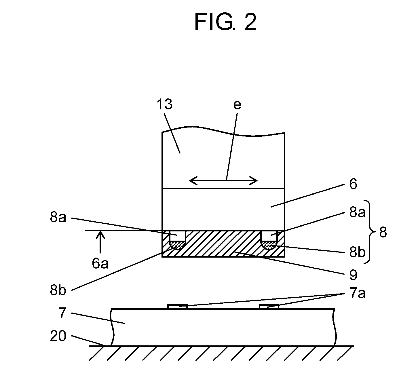
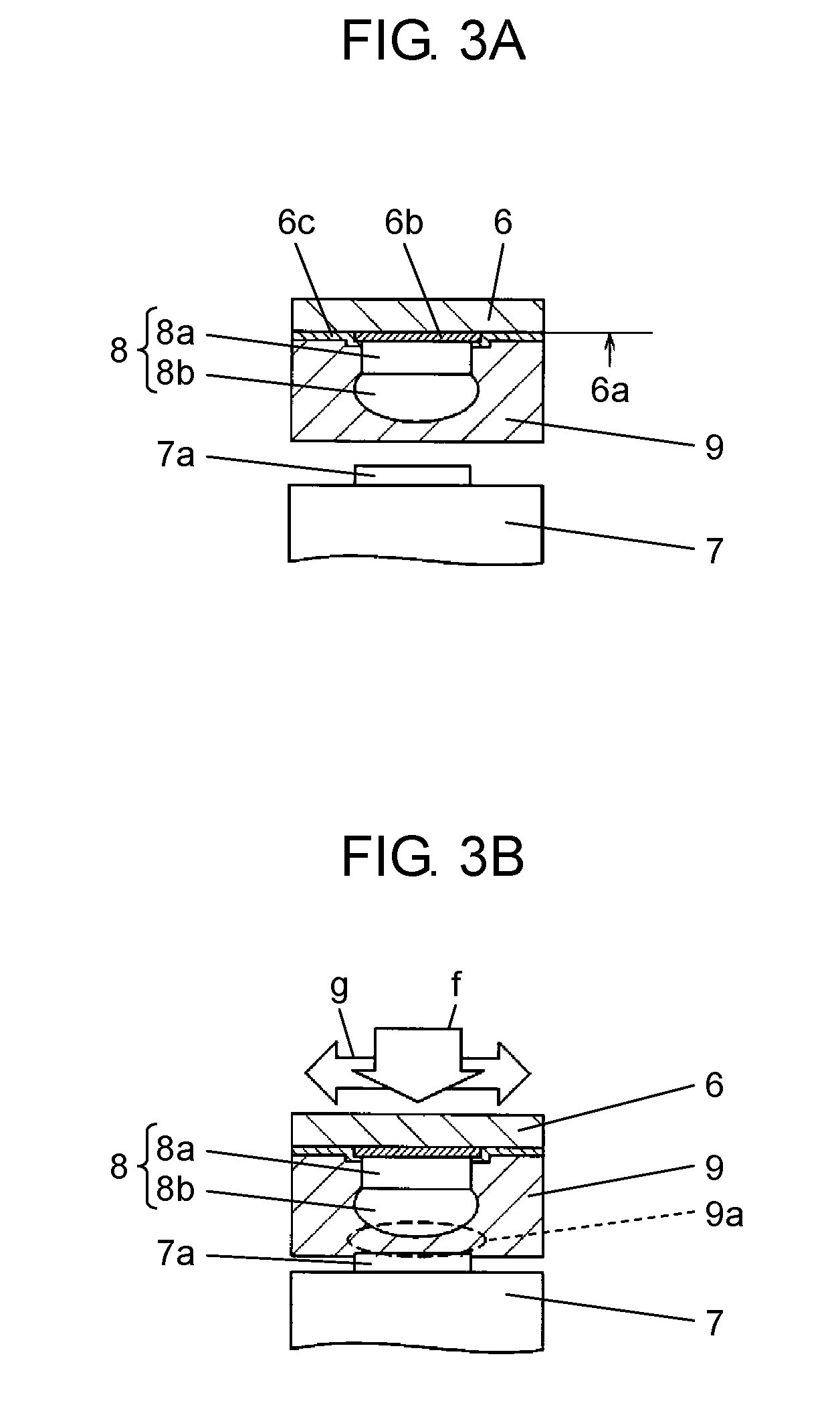
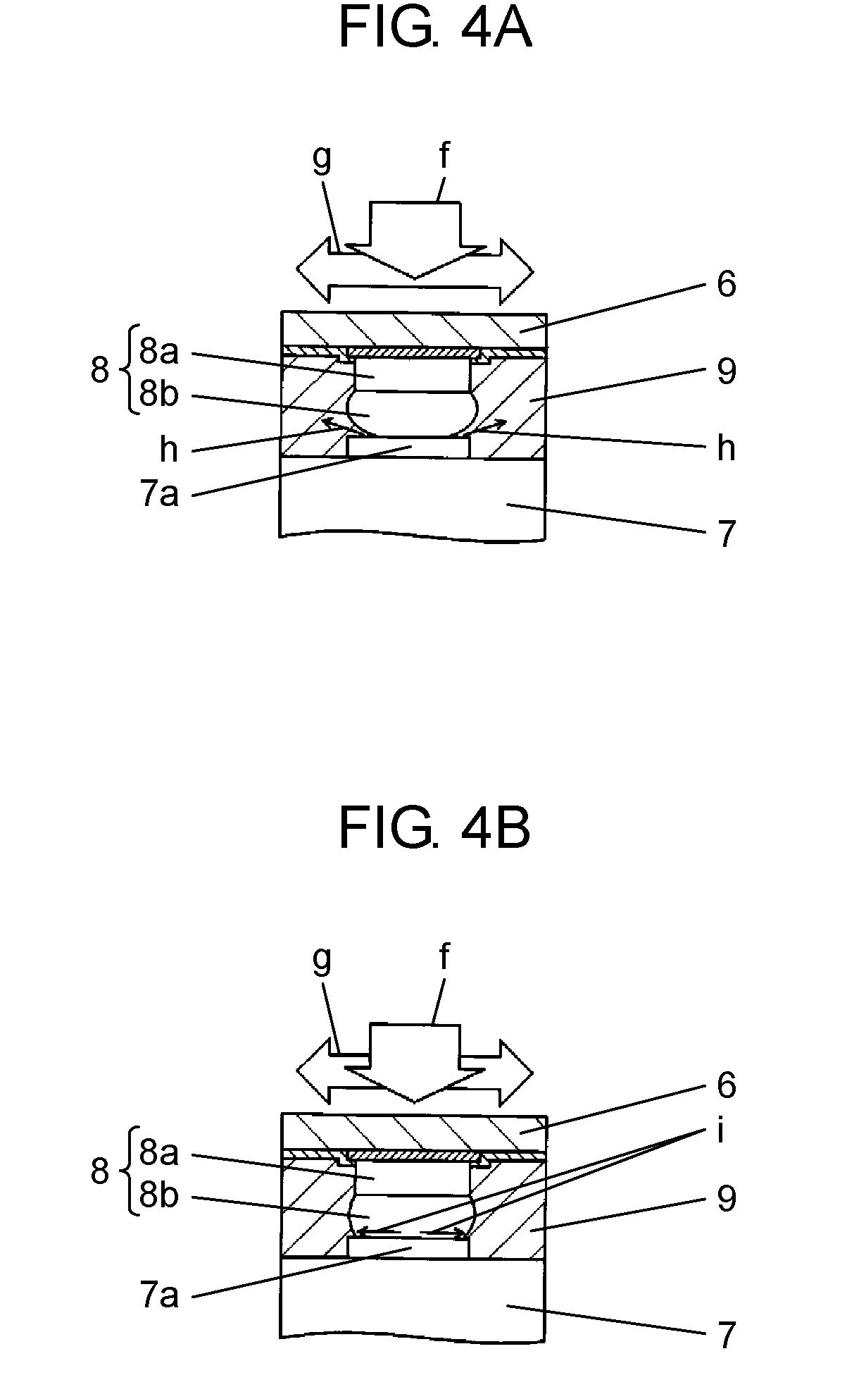
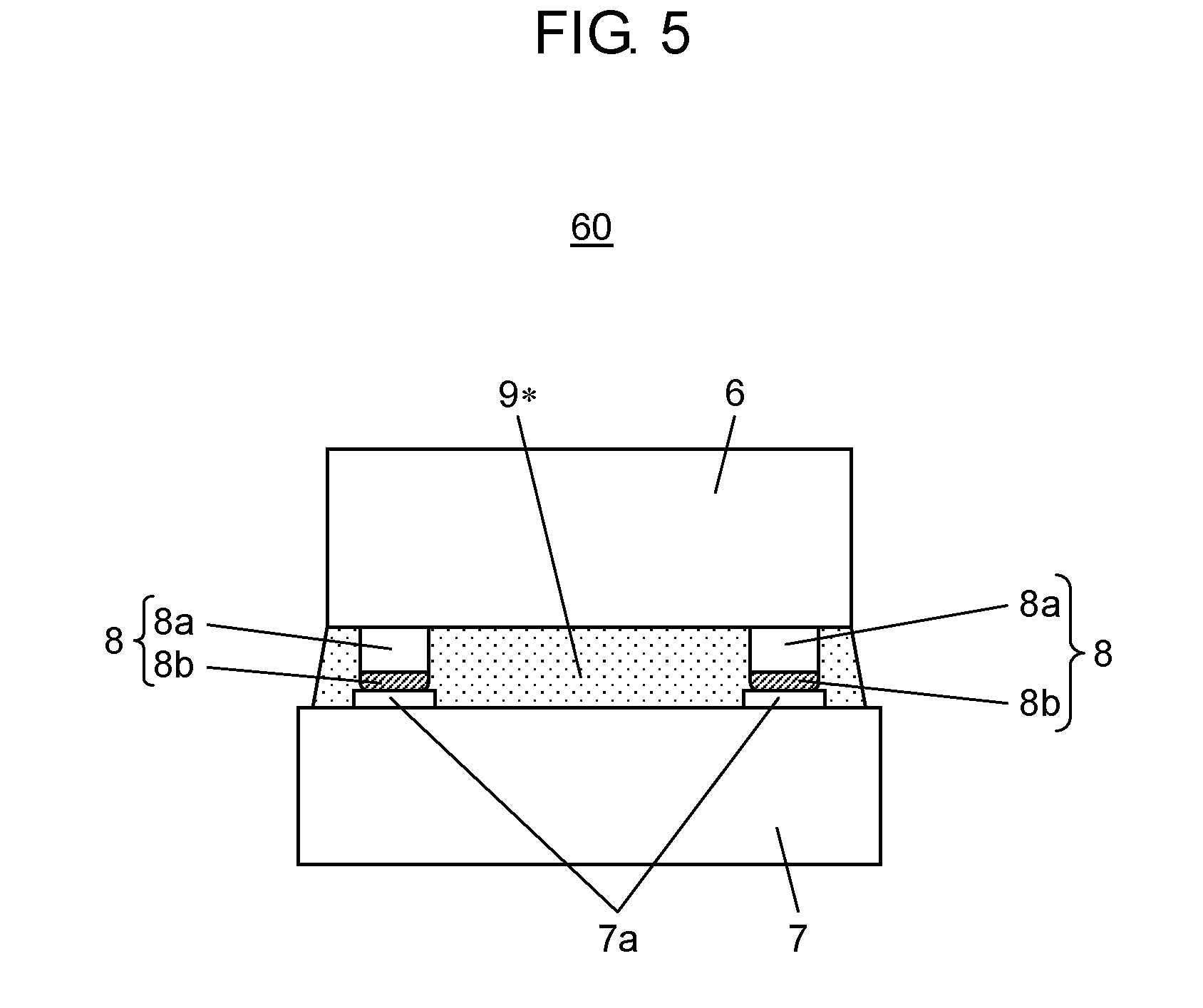
The present disclosure relates to a method of manufacturing a semiconductor device in which a bump of the semiconductor element is bonded to an electrode of a board. In a manufacturing process of the semiconductor device, by bonding a bump for external connection formed on a semiconductor element to an electrode of a board, a semiconductor element is mounted on the board. In a semiconductor device of such a configuration, for the purpose of fixing the semiconductor element and the board and reinforcing a junction portion between a bump and the electrode, a gap between the semiconductor element and the board is sealed with resin. As a component mounting method for a semiconductor element in manufacturing such a semiconductor device, there is known a technology in which a liquid resin for resin sealing is coated on the board so as to cover the electrode and the bump of the semiconductor element is bonded to the electrode by ultrasonic bonding via a liquid resin (for example, see Japanese Patent Unexamined Publication No. 2005-26579). In the related art described in the Japanese Patent Unexamined Publication No. 2005-26579, a liquid flux fill having both the act of flux and a function as underfill resin is coated on the board of a surface on which an electrode is formed. In this state, solder bumps formed on the electronic component and the electrodes are ultrasonically bonded. In this process, the solder bump is brought close to the electrode covered with the flux fill and the solder bump comes into contact with the electrode such that ultrasonic vibration energy acts to a contact portion between the solder bump and the electrode. A method of manufacturing a semiconductor device of the present disclosure includes a first step of preparing a semiconductor element including a functional surface on which a bump for external connection is formed and an adhesive layer of a film shape that covers the functional surface and the bump, and includes a flux component; a second step of positioning the semiconductor element in a state in which the bump and an electrode face each other above a board including the electrode to which the bump is bonded; a third step of activating the flux component of a portion of the adhesive layer sandwiched between the bump and the electrode by pressing the adhesive layer against the electrode and applying ultrasonic vibration to the semiconductor element; a fourth step of pushing out the flux component from the portion of the adhesive layer by pressing the semiconductor element while applying the ultrasonic vibration to the board and bringing the bump into contact with the electrode; and a fifth step of bonding the bump to the electrode by continuing the application of the ultrasonic vibration and the pressing of the semiconductor element. According to the present disclosure, it is possible to efficiently perform bonding of the bump and the electrode at a low temperature range by improving the act of removing an oxide film at a contact portion between the bump of the semiconductor element and the electrode of the board. Prior to describing an embodiment, a problem in the related art will be briefly described. The above-described related art has the following disadvantages due to the application of ultrasonic wave in a state where a solder bump is in contact with an electrode. That is, in the related art, when the ultrasonic waves are applied, most of flux fills are excluded from a contact portion between the solder bump and the electrode. Therefore, the removal of an oxide film by flux components with respect to a surface of the solder bump and the electrode does not sufficiently act, and bonding failure between the solder bump and the electrode is caused. As a countermeasure against such a problem, it may be considered to increase oxide film removing act by activating the flux fill by heating. However, in this case, a problem such as warp deformation due to heating of the electronic component of a bonding target occurs. Particularly, in a case where a manufactured target is a stacked type semiconductor device mounted by stacking thin semiconductor elements, in order to suppress deformation due to heat as much as possible, it is required to be able to perform ultrasonic bonding in a temperature range as low as possible. In view of the above, the present disclosure is to provide a method of manufacturing a semiconductor device capable of efficiently performing bonding of the bump and the electrode at a low temperature range by improving the act of removing an oxide film at a contact portion between the bump of the semiconductor element and an electrode of a board. Next, an embodiment of the present disclosure will be described with reference to the drawings. First, with reference to In Element holding table 10 capable of horizontally moving in X direction and Y direction by a horizontal moving mechanism (not shown) is provided in element supplier 2. A plurality of semiconductor elements 6 which are a target of the bonding in this embodiment are held on an upper surface of element holding table 10. Here, semiconductor elements 6 are held in a face-up posture in which functional surface 6 Here, a configuration of semiconductor element 6 will be described with reference to Here, bump 8 has a configuration in which solder 8 In functional surface 6 In order to achieve such a function, adhesive layer 9 has a composition including a main agent made of a resin, a thermoplastic agent, a curing agent for the resin, a curing accelerator, an organic acid, and a filler. The main agent, a thermosetting resin such as an epoxy resin is used. As a thermoplastic agent blended for forming a film, a phenoxy resin is used. As a curing agent for curing the resin, hydrazides, imidazoles, acid anhydrides or the like is used. In addition, as a curing accelerator for accelerating the curing of the resin, imidazole is used. Furthermore, as the organic acid which is the flux component that reduces and removes the oxide film at the junction portion, succinic acid, benzoic acid, adipic acid, salicylic acid or the like is used. As a filler for adjusting thermal expansion of cured adhesive layer 9, silica, alumina or the like is used. Substance types shown in the above composition are examples and other kinds of substances having the same act can also be used. Semiconductor elements 6 of the above-described structure are arranged on the upper surface of element holding table 10 in the face-up posture in which adhesive layer 9 faces upward in element supplier 2. These semiconductor elements 6 are sequentially extracted by element inverter 3, and transferred to bonding mechanism 4 after adhesive layer 9 is reversed to the downward in a face-down posture. As shown in By upwardly moving pickup nozzle 11 positioned downward with respect to element holding table 10 (arrow a), semiconductor element 6 held in element holding table 10 in the face-up posture can be extracted by being suck and held by pickup nozzle 11. Next, by driving reverse mechanism 3 Bonding mechanism 4 has a configuration in which bonding head 16 that performs the ultrasonic bonding by holding semiconductor element 6 moves in a horizontal direction and a vertical direction by bonding head movement mechanism 19. Camera 12 is disposed below a movement path of bonding head 16 by bonding head moving mechanism 19 with an imaging direction facing upward. Camera 12 images semiconductor element 6 held by holding nozzle 13 from below. By performing a recognition process on the imaged result by controller 21, true/false identification and a positional deviation state of semiconductor element 6 are detected. Bonding head 16 is configured by mounting vibrator 14 on one end portion of ultrasonic horn 15. Furthermore, bonding head 16 has holding nozzle 13 holding semiconductor element 6. Holding nozzle 13 is provided to extend downward from ultrasonic horn 15. By operating vibrator 14, the ultrasonic vibration is transferred to holding nozzle 13 via ultrasonic horn 15. Bonding head 16 is connected to bonding head movement mechanism 19 via head holder 17 and pressing mechanism 18 is incorporated in head holder 17. Pressing mechanism 18 has a load control function for controlling a pressing load when pressing semiconductor element 6 against board 7 by bonding head 16 and a contact detection function for detecting a timing at which semiconductor element 6 is in contact with board 7 in a bonding process. Board stage 20 for holding board 7 is provided on board positioner 5. In the bonding operation by bonding mechanism 4, the semiconductor elements 6 held by holding nozzle 13 are bonded on a plurality of the junction portions set on board 7 by sequentially ultrasonic bonding. In the bonding operation, vibrator 14 is operated while bump 8 of semiconductor element 6 held by holding nozzle 13 is pressed against electrode 7 The bonding device 1 includes controller 21 and controller 21 in the above-described configuration controls operations of element supplier 2, element inverter 3, bonding mechanism 4, and board positioner 5. In this operation control, controller 21 performs positioning with respect to board 7 of semiconductor element 6 at the time of the bonding operation by controlling bonding mechanism 4 by adding a position recognition result of semiconductor element 6 acquired by camera 12. In the bonding operation by bonding mechanism 4, first, bonding head 16 is moved above element inverter 3 by bonding head movement mechanism 19. Holding nozzle 13 is positioned above a transfer position of semiconductor element 6 by pickup nozzle 11. Next, bonding head 16 is lowered such that semiconductor element 6 of the face-down posture is sucked and held by holding nozzle 13. Next, by moving bonding head 16 above camera 12, semiconductor element 6 held by holding nozzle 13 is imaged by camera 12 (arrow c), and position recognition of semiconductor element 6 is performed. Next, bonding head 16 holding semiconductor element 6 after position recognition is moved above board 7 held on board stage 20 in board positioner 5, and semiconductor element 6 of the face-down posture is lowered to a predetermined bonding portion (arrow d). That is, as shown in Next, with reference to In the method of manufacturing the semiconductor device, first, semiconductor element 6 with an adhesive layer shown in Next, semiconductor element 6 of the above-described configuration is held by holding nozzle 13 (not shown) and semiconductor element 6 is moved above board 7 by moving bonding head 16 such that a bonding portion is positioned on board 7. That is, as shown in Next, the ultrasonic bonding process starts. That is, semiconductor element 6 held by holding nozzle 13 is lowered with respect to board 7. At a timing at which pressing mechanism 18 detects that adhesive layer 9 of semiconductor element 6 is brought into contact with electrode 7 That is, as shown in The above-described activation of the flux components is presumed to be due to the following mechanism. That is, by acting the physical force of the ultrasonic vibration to adhesive layer 9 to the activation target area 9 With this, the degree of contact of a reducing component such as organic acid contained in adhesive layer 9 with the joint surface via these cavities increases and as a result, the activation of the flux component is realized. In the activation of the flux components, since adhesive layer 9 as a whole is a film shape solid, even if the ultrasonic vibration acts before bump 8 of semiconductor element 6 is pressed against electrode 7 After activating the flux component of adhesive layer 9 in this manner, the ultrasonic bonding process proceeds. As shown in In this state, the ultrasonic bonding process is continued. That is, as shown in In the metal junction by the ultrasonic vibration, since the newly formed metal surfaces are bonded to each other by the mechanical energy of the ultrasonic vibration without melting solder 8 After that, board 7 on which a predetermined number of each of semiconductor elements 6 are mounted by the ultrasonic bonding is sent to a curing device (sixth process). In the curing device, by holding board 7 for a predetermined period of time in a temperature atmosphere higher than a thermal curing temperature of the main agent (here, epoxy resin) configuring adhesive layer 9, adhesive layer 9 is thermally cured. With this, for each semiconductor element 6, a gap between board 7 and semiconductor element 6 is sealed, and a resin sealing portion 9* (see As described above, in the method of manufacturing the semiconductor device indicated in this embodiment, as semiconductor element 6 mounted on board 7 by the ultrasonic bonding, on functional surface 6 It is possible to improve the act of removing the oxide film on the joint surface which is a contact portion between bump 8 and electrode 7 In the above-described embodiment, a configuration is shown in which solder 8 The method of manufacturing the semiconductor device of the present disclosure has an effect that it is possible to efficiently perform bonding of the bump and the electrode in the low temperature range and is useful in a manufacturing field of a semiconductor device in which the bump of the semiconductor element is bonded to the electrode of the board by improving the act of removing the oxide film in the contact portion between the bump of the semiconductor element and the electrode of the board. A method of manufacturing a semiconductor device includes a step of preparing a semiconductor element including a functional surface on which a bump is formed and an adhesive layer of a film shape including a flux component, a step of positioning the semiconductor element above a board including an electrode, a step of activating a flux component by applying ultrasonic vibration to the semiconductor element, a step of bringing the bump into contact with the electrode by pressing the semiconductor element to the board, and a step of bonding the bump to the electrode by continuing the application of the ultrasonic vibration and the pressing of the semiconductor element. 1. A method of manufacturing a semiconductor device, comprising:
a first step of preparing a semiconductor element including a functional surface on which a bump for external connection is formed and an adhesive layer of a film shape that covers the functional surface and the bump, the adhesive layer including a flux component; a second step of positioning the semiconductor element in a state in which the bump and an electrode face each other above a board including the electrode to which the bump is bonded; a third step of activating the flux component of a portion of the adhesive layer sandwiched between the bump and the electrode by pressing the adhesive layer against the electrode and applying ultrasonic vibration to the semiconductor element; a fourth step of pushing out the flux component from the portion of the adhesive layer by pressing the semiconductor element while applying the ultrasonic vibration to the board, and bringing the bump into contact with the electrode; and a fifth step of bonding the bump to the electrode by continuing the application of the ultrasonic vibration and the pressing of the semiconductor element. 2. The method of manufacturing the semiconductor device of wherein the adhesive layer includes a main agent made of a resin, a thermoplastic agent, a curing agent for curing the resin of the main agent, a curing accelerator for accelerating curing of the resin of the main agent, an organic acid, and a filler. 3. The method of manufacturing the semiconductor device of wherein a solder is formed on a surface of at least one of the bump and the electrode.BACKGROUND
1. Technical Field
2. Description of the Related Art
SUMMARY
BRIEF DESCRIPTION OF THE DRAWINGS
DETAILED DESCRIPTION