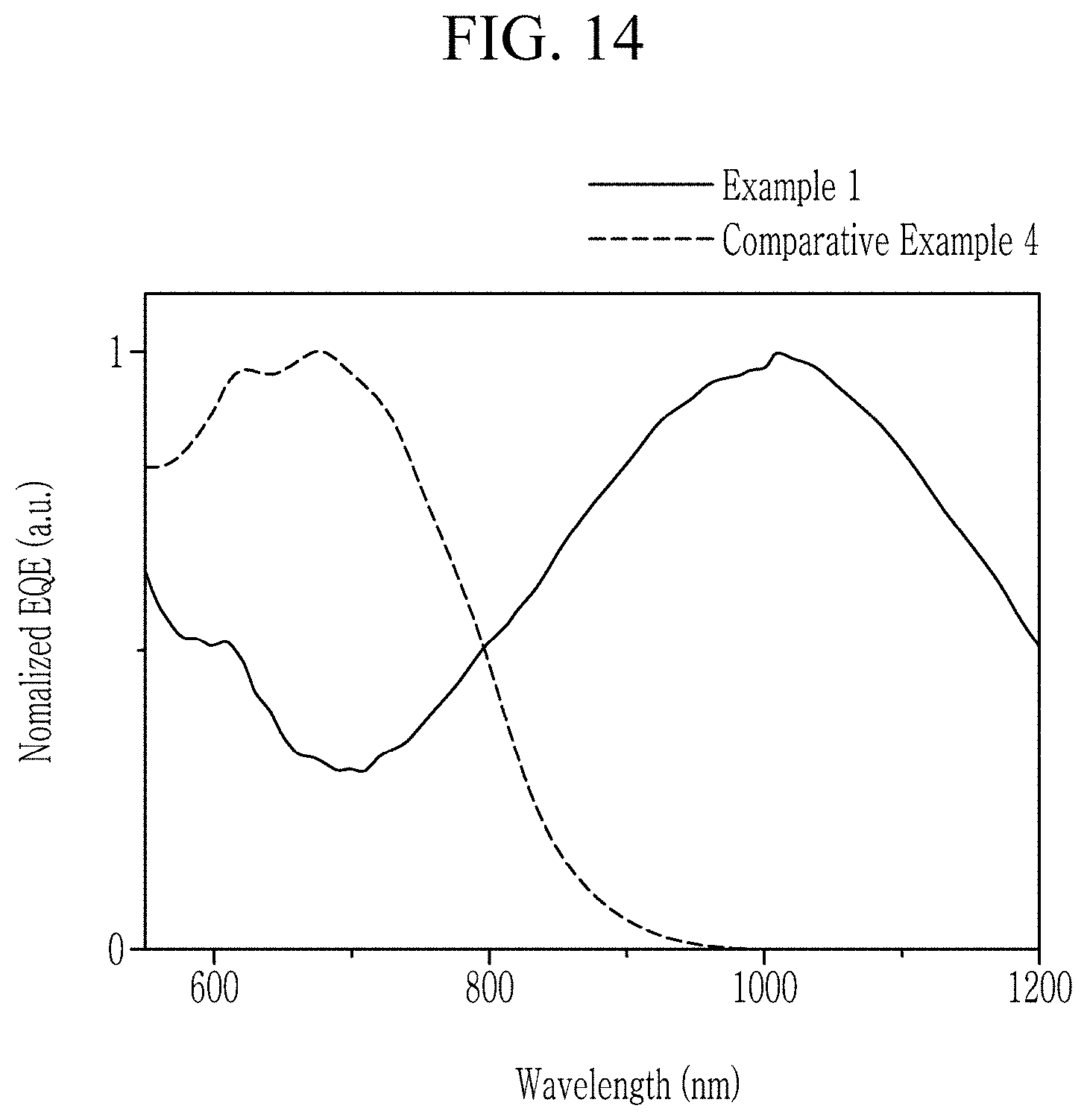
NEAR-INFRARED ABSORBERS, NEAR-INFRARED ABSORBING/BLOCKING FILMS, PHOTOELECTRIC DEVICES, ORGANIC SENSORS, AND ELECTRONIC DEVICES
This application claims priority to and the benefit of, under 35 U.S.C. § 119, Korean Patent Application No. 10-2019-0151737 filed in the Korean Intellectual Property Office on Nov. 22, 2019, and Korean Patent Application No. 10-2019-0152735 filed in the Korean Intellectual Property Office on Nov. 25, 2019, the entire contents of each of which are incorporated herein by reference. A near-infrared (NIR) absorber, a near-infrared absorbing/blocking film, a photoelectric device, an organic sensor, and an electronic device are disclosed. An imaging device is used in a digital camera and a camcorder, etc., to capture an image and to store it as an electrical signal, and the imaging device includes a sensor separating incident light according to a wavelength and converting each component to an electrical signal. Recently, photoelectric devices in the near-infrared region for improving sensitivity of a sensor in a low-illumination environment or for use as a biometric device have been studied. Some example embodiments provide a near-infrared absorber having improved near-infrared light absorption characteristics. Some example embodiments provide a film including the near-infrared absorber. Some example embodiments provide a photoelectric device including the near-infrared absorber. Some example embodiments provide an organic sensor including the near-infrared absorber or the photoelectric device. Some example embodiments provide an electronic device including the photoelectric device or the organic sensor. According to some example embodiments, a near-infrared absorber including a compound represented by Chemical Formula 1 is provided. In Chemical Formula 1, Ar is a substituted or unsubstituted C6 to C30 aromatic ring, a substituted or unsubstituted C3 to C30 heteroaromatic ring, or a combination thereof, X1is O, S, Se, Te, S(═O), S(═O2), NRa, CRbRc, SiRdRe, GeRfRg, CRhCRi, or CRhh═CRii(wherein Ra, Rb, Rc, Rd, Re, Rf, Rg, Rh, and Riare independently hydrogen, deuterium, a C1 to C30 alkyl group, a C1 to C30 haloalkyl group, a C6 to C30 aryl group, a C6 to C30 aryloxy group, a C3 to C30 heteroaryl group, a halogen, a cyano group, or a combination thereof, Rhhand Riiare independently (CH)wwhere w is a positive integer or at least one heteroatom of O, N, S, Se, or Te, and Rhhand Riiare linked to each other to form an aromatic ring or a heteroaromatic ring), X2is O, S, Se, Te, C, CRx—CRy, CRxx—CRyy, S(═O), or S(═O2) (wherein Rxand Ryare independently hydrogen, deuterium, a C1 to C30 alkyl group, a C1 to C30 haloalkyl group, a C6 to C30 aryl group, a C6 to C30 aryloxy group, a C3 to C30 heteroaryl group, a halogen, a cyano group, or a combination thereof, Rxxand Ryyare independently (CH)vwhere v is a positive integer or at least one heteroatom of O, N, S, Se, or Te, and Rxxand Ryyare linked to each other to form an aromatic ring or a heteroaromatic ring), Ar1and Ar2are independently a heteroarene group including at least one heteroatom of O, S, Se, or Te, Ar3and Ar4are independently a substituted or unsubstituted C6 to C30 arene group, a substituted or unsubstituted C3 to C30 heteroarene group, or a condensed ring group thereof, R1and R2are independently hydrogen, deuterium, a halogen, a cyano group, a nitro group, a hydroxyl group, a substituted or unsubstituted C1 to C10 alkyl group, a substituted or unsubstituted C1 to C10 alkoxy group, a substituted or unsubstituted C6 to C10 aryl group, or a substituted or unsubstituted C3 to C10 heteroaryl group, and L1and L2are independently a single bond, —O—, —S—, —Se—, —Te—, —N═, —NRa—, —SiRbRc—, —GeRdRe—, —(CRfRg)n—, or —(C(Rh)═C(Ri))— (wherein Ra, Rb, Rc, Rd, Re, Rf, Rg, Rh, and Riare independently hydrogen, deuterium, a halogen, a cyano group, a substituted or unsubstituted C1 to C10 alkyl group, or a substituted or unsubstituted C6 to C10 aryl group, wherein Rband Rc, Rdand Re, Rfand Rg, or Rhand Riare independently present or are linked to each other to form a separate ring, and n of —(CRfRg)n— is an integer of 1 or 2). In Chemical Formula 1, Ar may be benzene ring, a substituted or unsubstituted naphthalene ring, a substituted or unsubstituted anthracene ring, a substituted or unsubstituted phenanthrene ring, a substituted or unsubstituted tetracene ring, or a substituted or unsubstituted pyrene ring. In Chemical Formula 1, Ar may be a substituted or unsubstituted quinoline ring, a substituted or unsubstituted isoquinoline ring, a substituted or unsubstituted quinoxaline ring, a substituted or unsubstituted quinazoline ring, or a substituted or unsubstituted phenanthroline ring. In Chemical Formula 1, Ar may be one moiety of a set of moieties represented by Chemical Formula A-1, each moiety including at least one aromatic ring and left and right linking groups. In Chemical Formula A-1, hydrogen of each aromatic ring may be replaced by a halogen, a cyano group, a C1 to C10 alkyl group, a C1 to C10 alkoxy group, a C1 to C10 haloalkyl group, a silyl group, or a C1 to C10 alkylsilyl group, separate adjacent pairs of *'s inside the at least one aromatic ring are linking portions with separate, respective ones of an N—X1—N-containing ring of Chemical Formula 1 or —N═X2═N-containing ring of Chemical Formula 1, and *'s of the left and right linking groups are portions linked to separate, respective ones of Ar1or Ar2of Chemical Formula 1. In Chemical Formula 1, Ar may be one moiety of a set of moieties represented by Chemical Formula A-2, each moiety including at least one aromatic ring and left and right linking groups. In Chemical Formula A-2, hydrogen of each aromatic ring may be replaced by a halogen, a cyano group, a C1 to C10 alkyl group, a C1 to C10 alkoxy group, a C1 to C10 haloalkyl group, —SiH3, or a C1 to C10 alkylsilyl group, separate adjacent pairs of *'s inside the at least one aromatic ring are linking portions with separate, respective ones of an N—X1—N-containing ring of Chemical Formula 1 and —N═X2═N-containing ring of Chemical Formula 1, and *'s of the left and right linking groups are portions linked to separate, respective ones of Ar1and Ar2of Chemical Formula 1. In Chemical Formula 1, when X2is CRxx—CRyy, the aromatic ring formed by linking Rxxwith Ryymay be a substituted or unsubstituted benzene ring, a substituted or unsubstituted naphthalene ring, a substituted or unsubstituted acenaphthene ring, a substituted or unsubstituted anthracene ring, a substituted or unsubstituted phenanthrene ring, a substituted or unsubstituted tetracene ring or a substituted or unsubstituted pyrene ring; or a substituted or unsubstituted quinoline ring, a substituted or unsubstituted isoquinoline ring, a substituted or unsubstituted quinoxaline ring, a substituted or unsubstituted quinazoline ring, a substituted or unsubstituted phenanthroline ring, a substituted or unsubstituted pyrimidine ring, or a substituted or unsubstituted benzodithiophene ring. In Chemical Formula 1, when X2is CRxx—CRyy, the aromatic ring formed by linking Rxxwith Ryymay be one moiety of a set of moieties represented by Chemical Formula B-1, each moiety including at least one aromatic ring. In Chemical Formula B-1, hydrogen of each aromatic ring may be replaced by a halogen, a cyano group, a C1 to C30 alkyl group, a C1 to C30 alkoxy group, a C1 to C30 haloalkyl group, —SiH3, a C1 to C30 alkylsilyl group, a C6 to C30 aryl group, a C6 to C30 aryloxy group, or a C3 to C30 heteroaryl group, and *'s inside the at least one aromatic ring are linking portions with a carbon of CRxx—CRyy. In Chemical Formula 1, when X2is CRxx—CRyy, the aromatic ring formed by linking Rxxwith Ryymay be one moiety of a set of moieties represented by Chemical Formula B-2, each moiety including at least one aromatic ring. In Chemical Formula B-2, hydrogen of each aromatic ring may be replaced by a halogen, a cyano group, a C1 to C30 alkyl group, a C1 to C30 alkoxy group, a C1 to C30 haloalkyl group, —SiH3, a C1 to C30 alkylsilyl group, a C6 to C30 aryl group, a C6 to C30 aryloxy group, or a C3 to C30 heteroaryl group, and *'s inside the at least one aromatic ring are linking portions with a carbon of CRxx—CRyy. In Chemical Formula 1, when X2is CRxx—CRyy, the aromatic ring formed by linking Rxxwith Ryymay be one of moieties represented by Chemical Formulas B-3-1 and B-3-2. In Chemical Formulas B-3-1 and B-3-2, Ar11and Ar12are independently a substituted or unsubstituted C6 to C30 arene group or a substituted or unsubstituted C3 to C30 heteroarene group, in Chemical Formula B-3-1, Z1and Z2are independently CRaor N (wherein Rais hydrogen, deuterium, a C1 to C30 alkyl group, a C1 to C30 haloalkyl group, —SiH3, a C1 to C30 alkylsilyl group, —NH2, a C1 to C30 alkylamine group, a C6 to C30 arylamine group, a C6 to C30 aryl group, C6 to C30 aryloxy group, C3 to C30 heteroaryl group, a halogen, a cyano group, or a combination thereof), hydrogen of each aromatic ring may be replaced by a halogen, a cyano group, a C1 to C30 alkyl group, a C1 to C30 alkoxy group, a C1 to C30 haloalkyl group, —SiH3, a C1 to C30 alkylsilyl group, a C6 to C30 aryl group, a C6 to C30 aryloxy group, or a C3 to C30 heteroaryl group, and *'s inside the at least one aromatic ring are linking portions with a carbon of CRxx—CRyy. The moiety represented by Chemical Formula B-3-1 may be one moiety of a set of moieties represented by Chemical Formula B-3-11, each moiety including at least one aromatic ring. In Chemical Formula B-3-11, hydrogen of each aromatic ring may be replaced by a halogen, a cyano group, a C1 to C30 alkyl group, a C1 to C30 alkoxy group, a C1 to C30 haloalkyl group, —SiH3, a C1 to C30 alkylsilyl group, a C6 to C30 aryl group, a C6 to C30 aryloxy group, or a C3 to C30 heteroaryl group, and *'s inside the at least one aromatic ring are linking portions with the carbon of CRxx—CRyy. The moiety represented by Chemical Formula B-3-2 may be one moiety of a set of moieties represented by Chemical Formula B-3-21, each moiety including at least one aromatic ring. In Chemical Formula B-3-21, hydrogen of each aromatic ring may be replaced by a halogen, a cyano group, a C1 to C30 alkyl group, a C1 to C30 alkoxy group, a C1 to C30 haloalkyl group, —SiH3, a C1 to C30 alkylsilyl group, a C6 to C30 aryl group, a C6 to C30 aryloxy group, or a C3 to C30 heteroaryl group, Xaand Xbare independently O, S, Se, Te, NRa, SiRbRc, or GeRdRe(wherein Ra, Rb, Rc, Rd, and Reare independently hydrogen, a halogen, a cyano group, a substituted or unsubstituted C1 to C30 alkyl group, a substituted or unsubstituted C1 to C30 alkoxy group, a substituted or unsubstituted C6 to C30 aryl group, or a substituted or unsubstituted C6 to C30 aryloxy group), and *'s inside the aromatic ring are linking portions with the carbon of CRxx—CRyy. In Chemical Formula 1, Ar1and Ar2may be the same or different and may be each represented by one of Chemical Formula C-1-1, Chemical Formula C-1-2, or Chemical Formula C-1-3 that each include at least one aromatic ring. In Chemical Formulas C-1-1 to C-1-3, hydrogen of each aromatic ring may be replaced by a halogen, a cyano group, a C1 to C30 alkyl group, a C1 to C30 alkoxy group, a C1 to C30 haloalkyl group, —SiH3, a C1 to C30 alkylsilyl group, a C6 to C30 aryl group, a C6 to C30 aryloxy group, or a C3 to C30 heteroaryl group, Y1is O, S, Se, Te, S(═O), S(═O)2, NRa1, SiRb1Rc1, or GeRd1Re1(wherein Ra1, Rb1, Rc1, Rd1, and Re1are independently hydrogen, a C1 to C10 alkyl group, a C1 to C10 haloalkyl group, a C1 to C10 alkoxy group, —SiH3, a C1 to C10 alkylsilyl group, —NH3, a C1 to C10 alkylamine group, a C6 to C10 arylamine group, a C6 to C14 aryl group, a C6 to C14 aryloxy group, a C3 to C12 heteroaryl group, a halogen, a cyano group, or a combination thereof), Y2is O, S, Se, Te, S(═O), S(═O)2, NRa2, SiRb2Rc2, GeRd2Re2, or CRf2Rg2(wherein Ra2, Rb2, Rc2, Rd2, Re2, Rf2, and Rg2are independently hydrogen, a C1 to C10 alkyl group, a C1 to C10 haloalkyl group, a C1 to C10 alkoxy group, —SiH3, a C1 to C10 alkylsilyl group, —NH3, a C1 to C10 alkylamine group, a C6 to C10 arylamine group, a C6 to C14 aryl group, a C6 to C14 aryloxy group, a C3 to C12 heteroaryl group, a halogen, a cyano group, or a combination thereof), Rb1and Rc1, Rd1and Re1, Rb2and Rc2, Rd2and Re2, and Rf2and Rg2may be independently present or combined with each other to from a spiro ring, an * outside the at least one aromatic ring is a linking point with Ar of Chemical Formula 1, and *'s inside the at least one aromatic ring are linking portions with an N(R1)-containing ring that includes R1of Chemical Formula 1 and an N(R2)-containing ring that includes R2of Chemical Formula 1. In Chemical Formula 1, Ar1and Ar2are the same or different and may be each represented by one of Chemical Formulas C-2-1 to C-2-4 that each include at least one aromatic ring. In Chemical Formulas C-2-1 to C-2-4, hydrogen of each aromatic ring may be replaced by a halogen, a cyano group, a C1 to C30 alkyl group, a C1 to C30 alkoxy group, a C1 to C30 haloalkyl group, —SiH3, a C1 to C30 alkylsilyl group, a C6 to C30 aryl group, a C6 to C30 aryloxy group, or a C3 to C30 heteroaryl group, Y1is O, S, Se, Te, S(═O), S(═O)2, NRa1, SiRb1Rc1, or GeRd1Re1(wherein Ra1, Rb1, Rc1, Rd1, and Re1are independently hydrogen, a C1 to C10 alkyl group, a C1 to C10 haloalkyl group, a C1 to C10 alkoxy group, —SiH3, a C1 to C10 alkylsilyl group, —NH3, a C1 to C10 alkylamine group, a C6 to C10 arylamine group, a C6 to C14 aryl group, a C6 to C14 aryloxy group, a C3 to C12 heteroaryl group, a halogen, a cyano group, or a combination thereof), Rb1and Rc1and Rd1and Re1are independently present or combined with each other to from a spiro ring, an * outside the at least one aromatic ring is a linking point with Ar of Chemical Formula 1, and *'s inside the at least one aromatic ring are linking portions with an N(R1)-containing ring that includes R1of Chemical Formula 1 and an N(R2)-containing ring that includes R2of Chemical Formula 1. In Chemical Formula 1, Ar1and Ar2may be the same or different and may be each represented by one of Chemical Formulas C-3-1 to C-3-6 that each include at least one aromatic ring. In Chemical Formulas C-3-1 to C-3-6, hydrogen of each aromatic ring may be replaced by a halogen, a cyano group, a C1 to C30 alkyl group, a C1 to C30 alkoxy group, a C1 to C30 haloalkyl group, —SiH3, a C1 to C30 alkylsilyl group, a C6 to C30 aryl group, a C6 to C30 aryloxy group, or a C3 to C30 heteroaryl group, Y1is O, S, Se, Te, S(═O), S(═O)2, NRa1, SiRb1Rc1, or GeRd1Re1(wherein Ra1, Rb1, Rc1, Rd1and Re1are independently hydrogen, a C1 to C10 alkyl group, a C1 to C10 haloalkyl group, a C1 to C10 alkoxy group, —SiH3, a C1 to C10 alkylsilyl group, —NH3, a C1 to C10 alkylamine group, a C6 to C10 arylamine group, a C6 to C14 aryl group, a C6 to C14 aryloxy group, a C3 to C12 heteroaryl group, a halogen, a cyano group, or a combination thereof), Y2is O, S, Se, Te, S(═O), S(═O)2, NRa2, SiRb2Rc2, GeRd2Re2, or CRf2Rg2(wherein Ra2, Rb2, Rc2, Rd2, Re2, Rf2and Rg2are independently hydrogen, a C1 to C10 alkyl group, a C1 to C10 haloalkyl group, a C1 to C10 alkoxy group, —SiH3, a C1 to C10 alkylsilyl group, —NH3, a C1 to C10 alkylamine group, a C6 to C10 arylamine group, a C6 to C14 aryl group, a C6 to C14 aryloxy group, a C3 to C12 heteroaryl group, a halogen, a cyano group, or a combination thereof), Rb1and Rc1, Rd1and Re1, Rb2and Rc2, Rd2and Re2, and Rf2and Rg2may be independently present or combined with each other to from a spiro ring, an * outside the at least one aromatic ring is a linking point with Ar of Chemical Formula 1, and *'s inside the at least one aromatic ring are linking portions with an N(R1)-containing ring that includes R1of Chemical Formula 1 and an N(R2)-containing ring that includes R2of Chemical Formula 1. In Chemical Formula 1, Ar1and Ar2may be the same or different and may be each represented by one of Chemical Formula C-4-1 or Chemical Formula C-4-2 that each include at least one aromatic ring. In Chemical Formulas C-4-1 and C-4-2, hydrogen of each aromatic ring may be replaced by a halogen, a cyano group, a C1 to C30 alkyl group, a C1 to C30 alkoxy group, a C1 to C30 haloalkyl group, —SiH3, a C1 to C30 alkylsilyl group, a C6 to C30 aryl group, a C6 to C30 aryloxy group, or a C3 to C30 heteroaryl group, Y1is O, S, Se, Te, S(═O), S(═O)2, NRa1, SiRb1Rc1, or GeRd1Re1(wherein Ra1, Rb1, Rc1, Rd1and Re1are independently hydrogen, a C1 to C10 alkyl group, a C1 to C10 haloalkyl group, a C1 to C10 alkoxy group, —SiH3, a C1 to C10 alkylsilyl group, —NH3, a C1 to C10 alkylamine group, a C6 to C10 arylamine group, a C6 to C14 aryl group, a C6 to C14 aryloxy group, a C3 to C12 heteroaryl group, a halogen, a cyano group, or a combination thereof), Y2is O, S, Se, Te, S(═O), S(═O)2, NRa2, SiRb2Rc2, GeRd2Re2, or CRf2Rg2(wherein Ra2, Rb2, Rc2, Rd2, Re2, Rf2and Rg2are independently hydrogen, a C1 to C10 alkyl group, a C1 to C10 haloalkyl group, a C1 to C10 alkoxy group, —SiH3, a C1 to C10 alkylsilyl group, —NH3, a C1 to C10 alkylamine group, a C6 to C10 arylamine group, a C6 to C14 aryl group, a C6 to C14 aryloxy group, a C3 to C12 heteroaryl group, a halogen, a cyano group, or a combination thereof), Rb1and Rc1, Rd1and Re1, Rb2and Rc2, Rd2and Re2, and Rf2and Rg2may be independently present or combined with each other to from a spiro ring, an * outside the at least one aromatic ring is a linking point with Ar of Chemical Formula 1, and *'s inside the aromatic ring are linking portions with an N(R1)-containing ring that includes R1of Chemical Formula 1 and an N(R2)-containing ring that includes R2of Chemical Formula 1. In Chemical Formula 1, Ar1and Ar2may be the same or different and may be each represented by one of Chemical Formulas C-5-1 to C-5-8 that each include at least one aromatic ring. In Chemical Formulas C-5-1 to C-5-8, hydrogen of each aromatic ring may be replaced by a halogen, a cyano group, a C1 to C30 alkyl group, a C1 to C30 alkoxy group, a C1 to C30 haloalkyl group, —SiH3, a C1 to C30 alkylsilyl group, a C6 to C30 aryl group, a C6 to C30 aryloxy group, or a C3 to C30 heteroaryl group, Y1is O, S, Se, Te, S(═O), S(═O)2, NRa1, SiRb1Rc1, or GeRd1Re1(wherein Ra1, Rb1, Rc1, Rd1, and Re1are independently hydrogen, a C1 to C10 alkyl group, a C1 to C10 haloalkyl group, a C1 to C10 alkoxy group, —SiH3, a C1 to C10 alkylsilyl group, —NH3, a C1 to C10 alkylamine group, a C6 to C10 arylamine group, a C6 to C14 aryl group, a C6 to C14 aryloxy group, a C3 to C12 heteroaryl group, a halogen, a cyano group, or a combination thereof), Y2and Y3are independently O, S, Se, Te, S(═O), S(═O)2, NRa2, SiRb2Rc2, GeRd2Re2, or CRf2Rg2(wherein Ra2, Rb2, Rc2, Rd2, Re2, Rf2, and Rg2are independently hydrogen, a C1 to C10 alkyl group, a C1 to C10 haloalkyl group, a C1 to C10 alkoxy group, —SiH3, a C1 to C10 alkylsilyl group, —NH3, a C1 to C10 alkylamine group, a C6 to C10 arylamine group, a C6 to C14 aryl group, a C6 to C14 aryloxy group, a C3 to C12 heteroaryl group, a halogen, a cyano group, or a combination thereof), Rb1and Rc1, Rd1and Re1, Rb2and Rc2, Rd2and Re2, and Rf2and Rg2may be independently present or combined with each other to from a spiro ring, an * outside the at least one aromatic ring is a linking point with Ar of Chemical Formula 1, and *'s inside the at least one aromatic ring are linking portions with an N(R1)-containing ring that includes R1of Chemical Formula 1 and an N(R2)-containing ring that includes R2of Chemical Formula 1. A peak absorption wavelength of the near-infrared absorber may be in a wavelength region of about 750 nm to about 3000 nm. According to some example embodiments, a near-infrared absorbing/blocking film (absorbing and/or blocking film) including the near-infrared absorber is provided. According to some example embodiments, a photoelectric device includes a first electrode and a second electrode facing each other, and an active layer between the first electrode and the second electrode, wherein the active layer includes a near-infrared absorber including the compound represented by Chemical Formula 1. According to some example embodiments, an organic layer including the photoelectric device is provided. According to some example embodiments, an electronic device including the photoelectric device or the organic sensor is provided. According to some example embodiments, a photoelectric device may include a first electrode and a second electrode facing each other, an active layer between the first electrode and the second electrode, and a charge auxiliary layer between the active layer and the first electrode, or between the active layer and the second electrode. The charge auxiliary layer may include a near-infrared absorber that includes a compound represented by Chemical Formula 1: wherein, in Chemical Formula 1, Ar is a substituted or unsubstituted C6 to C30 aromatic ring, a substituted or unsubstituted C3 to C30 heteroaromatic ring, or a combination thereof, X1is O, S, Se, Te, S(═O), S(═O2), NRa, CRbRc, SiRdRe, GeRfRg, CRhCRi, or CRhh═CRII, wherein Ra, Rb, Rc, Rd, Re, Rf, Rg, Rh, and Riare independently hydrogen, deuterium, a C1 to C30 alkyl group, a C1 to C30 haloalkyl group, a C6 to C30 aryl group, a C6 to C30 aryloxy group, a C3 to C30 heteroaryl group, a halogen, a cyano group, or a combination thereof, Rhhand Riiare independently (CH)wor at least one heteroatom of O, N, S, Se, or Te where w is a positive integer, and Rhhand Riiare linked to each other to form an aromatic ring or a heteroaromatic ring, X2is O, S, Se, Te, C, CRx—CRy, CRxx—CRyy, S(═O) or S(═O2), wherein Rxand Ryare independently hydrogen, deuterium, a C1 to C30 alkyl group, a C1 to C30 haloalkyl group, a C6 to C30 aryl group, a C6 to C30 aryloxy group, a C3 to C30 heteroaryl group, a halogen, a cyano group, or a combination thereof, Rxxand Ryyare independently (CH)vwhere v is a positive integer or at least one heteroatom of O, N, S, Se, or Te, and Rxxand Ryyare linked to each other to form an aromatic ring or a heteroaromatic ring, Ar1and Ar2are independently a heteroarene group including at least one heteroatom of O, S, Se, or Te, Ar3and Ar4are independently a substituted or unsubstituted C6 to C30 arene group, a substituted or unsubstituted C3 to C30 heteroarene group, or a condensed ring group thereof, R1and R2are independently hydrogen, deuterium, a halogen, a cyano group, a nitro group, a hydroxyl group, a substituted or unsubstituted C1 to C10 alkyl group, a substituted or unsubstituted C1 to C10 alkoxy group, a substituted or unsubstituted C6 to C10 aryl group, or a substituted or unsubstituted C3 to C10 heteroaryl group, and L1and L2are independently a single bond, —O—, —S—, —Se—, —Te—, —N═, —NRa—, —SiRbRc—, —GeRdRe—, —(CRfRg)n—, or —(C(Rh)═C(Ri))—, wherein Ra, Rb, Rc, Rd, Re, Rf, Rg, Rh, and Riare independently hydrogen, deuterium, a halogen, a cyano group, a substituted or unsubstituted C1 to C10 alkyl group, or a substituted or unsubstituted C6 to C10 aryl group, wherein Rband Rc, Rdand Re, Rfand Rg, or Rhand Riare independently present or are linked to each other to form a separate ring, and n of —(CRfRg)n— is an integer of 1 or 2. The active layer may further include the near-infrared absorber. According to some example embodiments, an organic sensor may include a semiconductor substrate, a first photoelectric device on the semiconductor substrate, the first photoelectric device configured to selectively absorb light in a first near-infrared wavelength region, and an additional sensor configured to selectively absorb light in a separate wavelength region that is different from the first near-infrared wavelength region. The first photoelectric device may include a near-infrared absorber that includes a compound represented by Chemical Formula 1: wherein, in Chemical Formula 1, Ar is a substituted or unsubstituted C6 to C30 aromatic ring, a substituted or unsubstituted C3 to C30 heteroaromatic ring, or a combination thereof, X1is O, S, Se, Te, S(═O), S(═O2), NRa, CRbRc, SiRdRe, GeRfRg, CRhCRi, or CRhh═CRii, wherein Ra, Rb, Rc, Rd, Re, Rf, Rg, Rh, and Riare independently hydrogen, deuterium, a C1 to C30 alkyl group, a C1 to C30 haloalkyl group, a C6 to C30 aryl group, a C6 to C30 aryloxy group, a C3 to C30 heteroaryl group, a halogen, a cyano group, or a combination thereof, Rhhand Riiare independently (CH)wwhere w is a positive integer or at least one heteroatom of O, N, S, Se, or Te, and Rhhand Riiare linked to each other to form an aromatic ring or a heteroaromatic ring, X2is O, S, Se, Te, C, CRx—CRy, CRxx—CRyy, S(═O) or S(═O2), wherein Rxand Ryare independently hydrogen, deuterium, a C1 to C30 alkyl group, a C1 to C30 haloalkyl group, a C6 to C30 aryl group, a C6 to C30 aryloxy group, a C3 to C30 heteroaryl group, a halogen, a cyano group, or a combination thereof, Rxxand Ryyare independently (CH)vwhere v is a positive integer or at least one heteroatom of O, N, S, Se, or Te, and Rxxand Ryyare linked to each other to form an aromatic ring or a heteroaromatic ring, Ar1and Ar2are independently a heteroarene group including at least one heteroatom of O, S, Se, or Te, Ar3and Ar4are independently a substituted or unsubstituted C6 to C30 arene group, a substituted or unsubstituted C3 to C30 heteroarene group, or a condensed ring group thereof, R1and R2are independently hydrogen, deuterium, a halogen, a cyano group, a nitro group, a hydroxyl group, a substituted or unsubstituted C1 to C10 alkyl group, a substituted or unsubstituted C1 to C10 alkoxy group, a substituted or unsubstituted C6 to C10 aryl group, or a substituted or unsubstituted C3 to C10 heteroaryl group, and L1and L2are independently a single bond, —O—, —S—, —Se—, —Te—, —N═, —NRa—, —SiRbRc—, —GeRdRe—, —(CRfRg)n—, or —(C(Rh)═C(R1))—, wherein Ra, Rb, Rc, Rd, Re, Rf, Rg, Rh, and Riare independently hydrogen, deuterium, a halogen, a cyano group, a substituted or unsubstituted C1 to C10 alkyl group, or a substituted or unsubstituted C6 to C10 aryl group, wherein Rband Rc, Rdand Re, Rfand Rg, or Rhand Riare independently present or are linked to each other to form a separate ring, and n of —(CRfRg)n— is an integer of 1 or 2. The additional sensor may be an infrared light sensor at least partially embedded within the semiconductor substrate, and the separate wavelength region may be a separate near-infrared wavelength region that is different from the first near-infrared wavelength region, and the first photoelectric device and the infrared light sensor may overlap in a vertical direction that is perpendicular to a top surface of the semiconductor substrate. The additional sensor may include a plurality of photodiodes at least partially embedded within the semiconductor substrate, the plurality of photodiodes configured to selectively absorb light in separate visible wavelength regions, and the first photoelectric device and the plurality of photodiodes may overlap in a vertical direction that is perpendicular to a top surface of the semiconductor substrate. The organic sensor may further include an additional photoelectric device on the semiconductor substrate, the additional photoelectric device being between the first photoelectric device and the semiconductor substrate, the additional photoelectric device configured to selectively absorb light in an additional wavelength region that is different from the first near-infrared wavelength region and the separate visible wavelength regions. The additional sensor may include at least one additional photoelectric device vertically stacked between the first photoelectric device and the semiconductor substrate, each separate photoelectric device of the at least one additional photoelectric device including a separate photoelectric conversion layer and configured to selectively absorb light in a separate, respective wavelength region that is different from the first near-infrared wavelength region. The first photoelectric device may include a first electrode and a second electrode facing each other; and an active layer between the first electrode and the second electrode, wherein the active layer includes the near-infrared absorber. The first photoelectric device may include a first electrode and a second electrode facing each other; an active layer between the first electrode and the second electrode; and a charge auxiliary layer between the active layer and the first electrode, or between the active layer and the second electrode. The charge auxiliary layer may include the near-infrared absorber. The near-infrared absorber may exhibit good absorbing properties in the near-infrared region and thus, may be effectively used in photoelectric devices and/or organic sensors. Hereinafter, example embodiments will hereinafter be described in detail, and may be easily performed by a person having an ordinary skill in the related art. However, this disclosure may be embodied in many different forms and is not to be construed as limited to the example embodiments set forth herein. In the drawings, the thickness of layers, films, panels, regions, etc., are exaggerated for clarity. It will be understood that when an element such as a layer, film, region, or substrate is referred to as being “on” another element, it may be directly on the other element or intervening elements may also be present. In contrast, when an element is referred to as being “directly on” another element, there are no intervening elements present. It will further be understood that when an element is referred to as being “on” another element, it may be above or beneath the other element. It will be understood that elements and/or properties thereof may be recited herein as being “the same” or “equal” as other elements, and it will be further understood that elements and/or properties thereof recited herein as being “the same” as or “equal” to other elements may be “the same” as or “equal” to or “substantially the same” as or “substantially equal” to the other elements and/or properties thereof. Elements and/or properties thereof that are “substantially the same” as or “substantially equal” to other elements and/or properties thereof will be understood to include elements and/or properties thereof that are the same as or equal to the other elements and/or properties thereof within manufacturing tolerances and/or material tolerances. Elements and/or properties thereof that are the same or substantially the same as other elements and/or properties thereof may be structurally the same or substantially the same, functionally the same or substantially the same, and/or compositionally the same or substantially the same. It will be understood that elements and/or properties thereof described herein as being the “substantially” the same encompasses elements and/or properties thereof that have a relative difference in magnitude that is equal to or less than 10%. Further, regardless of whether elements and/or properties thereof are modified as “substantially,” it will be understood that these elements and/or properties thereof should be construed as including a manufacturing or operational tolerance (e.g., ±10%) around the stated elements and/or properties thereof. When the terms “about” or “substantially” are used in this specification in connection with a numerical value, it is intended that the associated numerical value include a tolerance of ±10% around the stated numerical value. When ranges are specified, the range includes all values therebetween such as increments of 0.1%. In the drawings, parts having no relationship with the description are omitted for clarity of the embodiments, and the same or similar constituent elements are indicated by the same reference numeral throughout the specification. As used herein, “at least one of A, B, or C,” “one of A, B, C, or a combination thereof” and “one of A, B, C, and a combination thereof” refer to each constituent element, and a combination thereof (e.g., A; B; C; A and B; A and C; B and C; or A, B, and C). Hereinafter, “combination” includes a mixture of two or more, inter-substitution, and a laminate structure of two or more. As used herein, when specific definition is not otherwise provided, “substituted” refers to replacement of a hydrogen of a compound or a functional group by a substituent selected from a halogen atom (F, Br, Cl, or I), a hydroxy group, a nitro group, a cyano group, an amino group, an azido group, an amidino group, an amine group (—NR′R″, wherein R′ and R″ are the same or different, and are a hydrogen atom, a C1 to C20 alkyl group, or a C6 to C30 aryl group), a hydrazino group, a hydrazono group, a carbonyl group, a carbamyl group, a thiol group, an ester group, a carboxyl group or a salt thereof, a sulfonic acid group or a salt thereof, a phosphoric acid group or a salt thereof, a silyl group (—SiR1R2R3, wherein R1to R3is hydrogen, a C1 to C10 alkyl group, or a C6 to C10 aryl group), a C1 to C20 alkyl group, a C1 to C20 alkoxy group, a C2 to C20 alkenyl group, a C2 to C20 alkynyl group, a C6 to C30 aryl group, a C7 to C30 arylalkyl group, a C1 to C30 alkoxy group, a C1 to C20 heteroalkyl group, a C3 to C20 heteroaryl group, a C3 to C20 heteroarylalkyl group, a C3 to C30 cycloalkyl group, a C3 to C15 cycloalkenyl group, a C6 to C15 cycloalkynyl group, a C3 to C30 heterocycloalkyl group, and a combination thereof. As used herein, when specific definition is not otherwise provided, “hetero” refers to one including 1 to 4 heteroatoms selected from N, O, S, Se, Te, Si, and P. As used herein, when a definition is not otherwise provided, “aromatic ring” refers to a functional group in which all atoms in the cyclic functional group have a p-orbital, and wherein these p-orbitals are conjugated and “heteroaromatic ring” refers to the aromatic ring including a heteroatom. The “aromatic ring” refers to a C6 to C30 arene group, for example a C6 to C20 arene group or a C6 to C30 aryl group, for example a C6 to C20 aryl group. The “heteroaromatic ring” refers to a C3 to C30 heteroarene group, for example a C3 to C20 heteroarene group or a C6 to C30 heteroaryl group, for example a C6 to C20 heteroaryl group. As used herein, “arene group” refers to a hydrocarbon ring group having an aromatic ring, and includes monocyclic and polycyclic hydrocarbon ring groups, and the additional ring of the polycyclic hydrocarbon ring group may be an aromatic ring or a nonaromatic ring. The arene group may be a C6 to C30 arene group, a C6 to C20 arene group, or a C6 to C10 arene group. The heteroarene group means an arene group including 1 to 3 heteroatoms selected from N, O, S, P, and Si in the ring. The heteroarene group may be a C3 to C30 heteroarene group, a C3 to C20 heteroarene group, or a C3 to C10 heteroarene group. As used herein, when a definition is not otherwise provided, “aryl group” refers to a group including at least one hydrocarbon aromatic moiety, and may include a group in which all elements of the hydrocarbon aromatic moiety have p-orbitals which form conjugation, for example a phenyl group, a naphthyl group, and the like; a group in which two or more hydrocarbon aromatic moieties may be linked by a sigma bond, for example a biphenyl group, a terphenyl group, a quarterphenyl group, and the like; and a group in which two or more hydrocarbon aromatic moieties are fused directly or indirectly to provide a non-aromatic fused ring, for example a fluorenyl group. The aryl group may include a monocyclic, polycyclic or fused polycyclic (i.e., rings sharing adjacent pairs of carbon atoms) functional group. As used herein, when a definition is not otherwise provided, “heteroaryl group” refers to an aryl group including at least one heteroatom selected from N, O, S, Se, Te, P, and Si instead of carbon (C) in the ring. When the heteroaryl group is a fused ring, at least one of rings of the heteroaryl group may have a heteroatom or each ring may have a heteroatom. As used herein, when a definition is not otherwise provided, “ring” refers to an aromatic ring, a non-aromatic ring, a heteroaromatic ring, a hetero non-aromatic ring, a fused ring thereof, and/or a combination thereof. The aromatic ring are the same as described above and the non-aromatic ring may be a C3 to C30 cycloalkyl group, a C3 to C30 cycloalkenyl group, or a C3 to C30 cycloalkynyl group. As used herein, when a definition is not otherwise provided, “halogen” may be one of F, Cl, Br, or I and the haloalkyl group may be an alkyl group in which at least one hydrogen is replaced by a halogen and may be, for example, a perfluoroalkyl group such as —CF3. Hereinafter, a near-infrared absorber according to some example embodiments is described. The near-infrared absorber may be referred to herein interchangeably as a “near-infrared absorbing compound.” The near-infrared absorber includes a compound represented by Chemical Formula 1. In Chemical Formula 1, Ar is a substituted or unsubstituted C6 to C30 aromatic ring, a substituted or unsubstituted C3 to C30 heteroaromatic ring, or a combination thereof, X1is O, S, Se, Te, S(═O), S(═O)2, NRa, CRbRc, SiRdRe, GeRfRg, CRhCRi, or CRhh═CRii(wherein Ra, Rb, Rc, Rd, Re, Rf, Rg, Rh, and Riare independently hydrogen, deuterium, a C1 to C30 alkyl group, a C1 to C30 haloalkyl group, a C6 to C30 aryl group, a C6 to C30 aryloxy group, a C3 to C30 heteroaryl group, a halogen, a cyano group, or a combination thereof, Rhhand Riiare independently (CH)wwhere w is a positive integer or at least one heteroatom of O, N, S, Se, or Te, and Rhhand Riiare linked to each other to form an aromatic ring or a heteroaromatic ring), X2is O, S, Se, Te, C, CRx—CRy, CRxx—CRyy, S(═O) or S(═O2) (wherein Rxand Ryare independently hydrogen, deuterium, a C1 to C30 alkyl group, a C1 to C30 haloalkyl group, a C6 to C30 aryl group, a C6 to C30 aryloxy group, a C3 to C30 heteroaryl group, a halogen, a cyano group, or a combination thereof, Rxxand Ryyare independently (CH)vwhere v is a positive integer or at least one heteroatom of O, N, S, Se, or Te, and Rxxand Ryyare linked to each other to form an aromatic ring or a heteroaromatic ring), Ar1and Ar2are independently a heteroarene group including at least one heteroatom of O, S, Se, or Te, Ar3and Ar4are independently a substituted or unsubstituted C6 to C30 arene group, a substituted or unsubstituted C3 to C30 heteroarene group, or a condensed ring group thereof, R1and R2are independently hydrogen, deuterium, a halogen, a cyano group, a nitro group, a hydroxyl group, a substituted or unsubstituted C1 to C10 alkyl group, a substituted or unsubstituted C1 to C10 alkoxy group, a substituted or unsubstituted C6 to C10 aryl group, or a substituted or unsubstituted C3 to C10 heteroaryl group, L1and L2are independently a single bond, —O—, —S—, —Se—, —Te—, —N═, —NRa—, —SiRbRc—, —GeRdRe—, —(CRfRg)n—, or —(C(Rh)═C(R1))— (wherein Ra, Rb, Rc, Rd, Re, Rf, Rg, Rh, and Riare independently hydrogen, deuterium, a halogen, a cyano group, a substituted or unsubstituted C1 to C10 alkyl group, or a substituted or unsubstituted C6 to C10 aryl group, wherein Rband Rc, Rdand Re, Rfand Rg, or Rhand R′ are independently present or are linked to each other to form a separate ring, and n of —(CRfRg)n— is an integer of 1 or 2). It is desirable that a material absorbing light in a long wavelength like the near-infrared light has small HOMO-LUMO bandgap energy, also referred to herein as small bandgap energy, low bandgap energy, or the like. In order to have the small bandgap energy, a conjugation length thereof may be made to be longer, but when the conjugation length becomes long, a deposition process is difficult to apply. The near-infrared absorber represented by Chemical Formula 1 has a donor-acceptor-donor structure that a core of a conjugation structure having electron-accepting characteristics (Ar-containing ring in Chemical Formula 1) is linked to an aromatic fused ring having electron-donating characteristics (Ar1-(a ring including N(R1) and L1)-Ar3) and (Ar2-(a ring including N(R2) and L2)-Ar4), and thus the near-infrared absorber has strong charge transfer characteristics and may effectively absorb light in a near-infrared wavelength region due to low bandgap energy. In addition, the near-infrared absorber has improved thermal stability and may be appropriate for a deposition process. Accordingly, a layer and/or structure that includes the near-infrared absorber may have improved sensitivity to and/or absorbance of light in the near-infrared wavelength region. A device configured to selectively absorb and/or convert (into electrical signals, e.g., photoelectrically convert) near-infrared light (e.g., a sensor) may have improved performance and/or efficiency based on including the near-infrared absorber, for example in an active layer configured to selectively absorb and/or convert (into electrical signals, e.g., photoelectrically convert) said near-infrared light. Hereinafter, the “ring including N(R1) and L1” may be called to be an “N(R1)-containing ring,” and the “ring including N(R2) and L2” may be called to be an “N(R2)-containing ring.” The “N(R1)-containing ring” and “ring including N(R2) and L2” may be individually a pentagonal ring (e.g., a substituted or unsubstituted pyrrole ring), a hexagonal ring (e.g., a substituted or unsubstituted pyridine ring, a substituted or unsubstituted oxazine ring, a substituted or unsubstituted thiazine ring, a substituted or unsubstituted selenoazine ring, or a substituted or unsubstituted pyrazine ring), or a heptagonal ring (e.g., a substituted or unsubstituted azepine ring) depending on L1and L2. In Chemical Formula 1, Ar may be benzene ring, a substituted or unsubstituted naphthalene ring, a substituted or unsubstituted anthracene ring, a substituted or unsubstituted phenanthrene ring, a substituted or unsubstituted tetracene ring, or a substituted or unsubstituted pyrene ring. In Chemical Formula 1, Ar may be a substituted or unsubstituted quinoline ring, a substituted or unsubstituted isoquinoline ring, a substituted or unsubstituted quinoxaline ring, a substituted or unsubstituted quinazoline ring, or a substituted or unsubstituted phenanthroline ring. In Chemical Formula 1, Ar may be one moiety of a set of moieties represented by Chemical Formula A-1, each moiety including at least one aromatic ring and left and right linking groups. In Chemical Formula A-1, hydrogen of each aromatic ring may be replaced by a halogen, a cyano group, a C1 to C10 alkyl group, a C1 to C10 alkoxy group, a C1 to C10 haloalkyl group, —SiH3, or a C1 to C10 alkylsilyl group, separate adjacent pairs of *'s inside the at least one aromatic ring are linking portions with separate, respective ones of an N—X1—N-containing ring of Chemical Formula 1 or —N═X2═N-containing ring of Chemical Formula 1, and *'s of the left and right linking groups are portions linked to separate, respective ones of Ar1or Ar2of Chemical Formula 1. In Chemical Formula 1, Ar may be one moiety of a set of moieties represented by Chemical Formula A-2, each moiety including at least one aromatic ring and left and right linking groups. In Chemical Formula A-2, hydrogen of each aromatic ring may be replaced by a halogen, a cyano group, a C1 to C10 alkyl group, a C1 to C10 alkoxy group, a C1 to C10 haloalkyl group, —SiH3, or a C1 to C10 alkylsilyl group, separate adjacent pairs of *'s inside the at least one aromatic ring are linking portions with separate, respective ones of an N—X1—N-containing ring of Chemical Formula 1 or —N═X2═N-containing ring of Chemical Formula 1, and *'s of the left and right linking groups are portions linked to separate, respective ones of Ar1or Ar2of Chemical Formula 1. In Chemical Formula 1, when X2is CRxx—CRyy, Rxxand Ryymay be linked to each other to form an aromatic ring. In this way, when the aromatic ring is further fused, an absorption wavelength of the compound is shifted to a long wavelength and stability of the compound may be increased. The aromatic ring may be substituted or unsubstituted benzene ring, a substituted or unsubstituted naphthalene ring, a substituted or unsubstituted acenaphthene ring, a substituted or unsubstituted anthracene ring, a substituted or unsubstituted phenanthrene ring, a substituted or unsubstituted tetracene ring or a substituted or unsubstituted pyrene ring; or a substituted or unsubstituted quinoline ring, a substituted or unsubstituted isoquinoline ring, a substituted or unsubstituted quinoxaline ring, a substituted or unsubstituted quinazoline ring, a substituted or unsubstituted phenanthroline ring, a substituted or unsubstituted pyrimidine ring, or a substituted or unsubstituted benzodithiophene ring. The aromatic ring may be one moiety of a set of moieties represented by Chemical Formula B-1, each moiety including at least one aromatic ring. In Chemical Formula B-1, hydrogen of each aromatic ring may be replaced by a halogen, a cyano group, a C1 to C30 alkyl group (e.g., a C1 to C20 alkyl group or a C1 to C10 alkyl group), a C1 to C30 alkoxy group (e.g., a C1 to C20 alkoxy group or a C1 to C10 alkoxy group), a C1 to C30 haloalkyl group (e.g., a C1 to C20 haloalkyl group or a C1 to C10 haloalkyl group), —SiH3, a C1 to C30 alkylsilyl group (e.g., a C1 to C20 alkylsilyl group or a C1 to C10 alkylsilyl group), a C6 to C30 aryl group (e.g., a C6 to C20 aryl group or a C6 to C10 aryl group), a C6 to C30 aryloxy group (e.g., a C6 to C20 aryloxy group or a C6 to C10 aryloxy group), or a C3 to C30 heteroaryl group (e.g., a C3 to C20 heteroaryl group or a C3 to C10 heteroaryl group), and *'s inside the at least one aromatic ring are linking portions with a carbon of CRxx—CRyy. The at least one aromatic ring may be one moiety of a set of moieties represented by Chemical Formula B-2, each moiety including at least one aromatic ring. In Chemical Formula B-2, hydrogen of each aromatic ring may be replaced by a halogen, a cyano group, a C1 to C30 alkyl group (e.g., a C1 to C20 alkyl group or a C1 to C10 alkyl group), a C1 to C30 alkoxy group (e.g., a C1 to C20 alkoxy group or a C1 to C10 alkoxy group), a C1 to C30 haloalkyl group (e.g., a C1 to C20 haloalkyl group or a C1 to C10 haloalkyl group), —SiH3, a C1 to C30 alkylsilyl group (e.g., a C1 to C20 alkylsilyl group or a C1 to C10 alkylsilyl group), a C6 to C30 aryl group (e.g., a C6 to C20 aryl group or a C6 to C10 aryl group), a C6 to C30 aryloxy group (e.g., a C6 to C20 aryloxy group or a C6 to C10 aryloxy group), or a C3 to C30 heteroaryl group (e.g., a C3 to C20 heteroaryl group or a C3 to C10 heteroaryl group), and *'s inside the at least one aromatic ring are linking portions with a carbon of CRxx—CRyy. The aromatic ring may be a moiety represented by Chemical Formulas B-3-1 or Chemical Formula B-3-2, each moiety including at least one aromatic ring. In Chemical Formulas B-3-1 and B-3-2, Ar11and Ar12are independently a substituted or unsubstituted C6 to C30 arene group or a substituted or unsubstituted C3 to C30 heteroarene group. In Chemical Formula B-3-1, Z1and Z2are independently CRaor N (wherein Rais hydrogen, deuterium, a C1 to C30 alkyl group (e.g., a C1 to C20 alkyl group or a C1 to C10 alkyl group), a C1 to C30 alkoxy group (e.g., a C1 to C20 alkoxy group or a C1 to C10 alkoxy group), a C1 to C30 haloalkyl group (e.g., a C1 to C20 haloalkyl group or a C1 to C10 haloalkyl group), —SiH3, a C1 to C30 alkylsilyl group (e.g., a C1 to C20 alkylsilyl group or a C1 to C10 alkylsilyl group), —NH2, a C1 to C30 alkylamine group (e.g., a C1 to C20 alkylamine group or a C1 to C10 alkylamine group), a C6 to C30 arylamine group (e.g., a C6 to C20 arylamine group or a C6 to C10 arylamine group), a C6 to C30 aryl group (e.g., a C6 to C20 aryl group or a C6 to C10 aryl group), a C6 to C30 aryloxy group (e.g., a C6 to C20 aryloxy group or a C6 to C10 aryloxy group), a C3 to C30 heteroaryl group, a halogen, a cyano group, or a combination thereof), and *'s inside the at least one aromatic ring are linking portions with a carbon of CRxx—CRyy. A moiety represented by Chemical Formula B-3-1 may be one moiety of a set of moieties represented by Chemical Formula B-3-11, each moiety including at least one aromatic ring. In Chemical Formula B-3-11, hydrogen of each aromatic ring may be replaced by a halogen, a cyano group, a C1 to C30 alkyl group (e.g., a C1 to C20 alkyl group or a C1 to C10 alkyl group), a C1 to C30 alkoxy group (e.g., a C1 to C20 alkoxy group or a C1 to C10 alkoxy group), a C1 to C30 haloalkyl group (e.g., a C1 to C20 haloalkyl group or a C1 to C10 haloalkyl group), —SiH3, a C1 to C30 alkylsilyl group (e.g., a C1 to C20 alkylsilyl group or a C1 to C10 alkylsilyl group), a C6 to C30 aryl group (e.g., a C6 to C20 aryl group or a C6 to C10 aryl group), a C6 to C30 aryloxy group (e.g., a C6 to C20 aryloxy group or a C6 to C10 aryloxy group), or a C3 to C30 heteroaryl group (e.g., a C3 to C20 heteroaryl group or a C3 to C10 heteroaryl group), and *'s inside the at least one aromatic ring are linking portions with the carbon of CRxx—CRyy. A moiety represented by Chemical Formula B-3-2 may be one moiety of a set of moieties represented by Chemical Formula B-3-21, each moiety including at least one aromatic ring. In Chemical Formula B-3-21, hydrogen of each aromatic ring may be replaced by a halogen, a cyano group, a C1 to C30 alkyl group (e.g., a C1 to C20 alkyl group or a C1 to C10 alkyl group), a C1 to C30 alkoxy group (e.g., a C1 to C20 alkoxy group or a C1 to C10 alkoxy group), a C1 to C30 haloalkyl group (e.g., a C1 to C20 haloalkyl group or a C1 to C10 haloalkyl group), —SiH3, a C1 to C30 alkylsilyl group (e.g., a C1 to C20 alkylsilyl group or a C1 to C10 alkylsilyl group), a C6 to C30 aryl group (e.g., a C6 to C20 aryl group or a C6 to C10 aryl group), a C6 to C30 aryloxy group (e.g., a C6 to C20 aryloxy group or a C6 to C10 aryloxy group), or a C3 to C30 heteroaryl group (e.g., a C3 to C20 heteroaryl group or a C3 to C10 heteroaryl group), Xaand Xbare independently O, S, Se, Te, NRa, SiRbRc, or GeRdRe(wherein Ra, Rb, Rc, Rd, and Reare independently hydrogen, a halogen, a cyano group, a substituted or unsubstituted C1 to C30 alkyl group (e.g., a C1 to C20 alkyl group or a C1 to C10 alkyl group), a substituted or unsubstituted C1 to C30 alkoxy group (e.g., a C1 to C20 alkoxy group or a C1 to C10 alkoxy group), a substituted or unsubstituted C6 to C30 aryl group (e.g., a C6 to C20 aryl group or a C6 to C10 aryl group), or a substituted or unsubstituted C6 to C30 aryloxy group (e.g., a C6 to C20 aryloxy group or a C6 to C10 aryloxy group)), and *'s inside the at least one aromatic ring are linking portions with the carbon of CRxx—CRyy. For example, in Chemical Formulas B-3-11 and B-3-21, halogen may be any of F, Cl, Br, and I, and the haloalkyl group may be an alkyl group in which at least one hydrogen is replaced by a halogen, for example, a perfluoroalkyl group such as —CF3. In Chemical Formula 1, Ar1and Ar2are heteroatom-containing ring groups, and the heteroatoms included in the rings may reinforce charge transfer characteristics and decrease bandgap energy. In addition, the number of aromatic rings of Ar1and Ar2may be changed to easily adjust an absorption wavelength. Since the structure that the plurality of aromatic rings is fused (Ar1-(the ring including N(R1) and L1)-Ar3) and (Ar2-(the ring including N(R2) and L2)-Ar4) provides a donor structure and thus increases a length of the conjugation structure, light of a long wavelength in a near-infrared region may be absorbed. In Chemical Formula 1, Ar1and Ar2may be the same or different and may each be represented by one of Chemical Formula C-1-1, Chemical Formula C-1-2, or Chemical Formula C-1-3 that each include at least one aromatic ring. In Chemical Formulas C-1-1 to C-1-3, hydrogen of each aromatic ring may be replaced by a halogen, a cyano group, a C1 to C30 alkyl group (e.g., a C1 to C20 alkyl group or a C1 to C10 alkyl group), a C1 to C30 alkoxy group (e.g., a C1 to C20 alkoxy group or a C1 to C10 alkoxy group), a C1 to C30 haloalkyl group (e.g., a C1 to C20 haloalkyl group or a C1 to C10 haloalkyl group), —SiH3, a C1 to C30 alkylsilyl group (e.g., a C1 to C20 alkylsilyl group or a C1 to C10 alkylsilyl group), a C6 to C30 aryl group (e.g., a C6 to C20 aryl group or a C6 to C10 aryl group), a C6 to C30 aryloxy group (e.g., a C6 to C20 aryloxy group or a C6 to C10 aryloxy group), or a C3 to C30 heteroaryl group (e.g., a C3 to C20 heteroaryl group or a C3 to C10 heteroaryl group), Y1is O, S, Se, Te, S(═O), S(═O)2, NRa1, SiRb1Rc1, or GeRd1Re1(wherein Ra1, Rb1, Rc1, Rd1, and Re1are independently hydrogen, a C1 to C10 alkyl group, a C1 to C10 haloalkyl group, a C1 to C10 alkoxy group, —SiH3, a C1 to C10 alkylsilyl group, —NH3, a C1 to C10 alkylamine group, a C6 to C10 arylamine group, a C6 to C14 aryl group, a C6 to C14 aryloxy group, a C3 to C12 heteroaryl group, a halogen, a cyano group, or a combination thereof), Y2is O, S, Se, Te, S(═O), S(═O)2, NRa2, SiRb2Rc2, GeRd2Re2, or CRf2Rg2(wherein Ra2, Rb2, Rc2, Rd2, Re2, Rf2, and Rg2are independently hydrogen, a C1 to C10 alkyl group, a C1 to C10 haloalkyl group, a C1 to C10 alkoxy group, —SiH3, a C1 to C10 alkylsilyl group, —NH3, a C1 to C10 alkylamine group, a C6 to C10 arylamine group, a C6 to C14 aryl group, a C6 to C14 aryloxy group, a C3 to C12 heteroaryl group, a halogen, a cyano group, or a combination thereof), Rb1and Rc1, Rd1and Re1, Rb2and Rc2, Rd2and Re2, and Rf2and Rg2may be independently present or combined with each other to from a spiro ring (e.g., a C4 to C8 cycloalkyl group, a C5 cycloalkyl group, or a C6 cycloalkyl group), an * outside the at least one aromatic ring is a linking point with Ar of Chemical Formula 1, and *'s inside the at least one aromatic ring are linking portions with an N(R1)-containing ring that includes R1of Chemical Formula 1 and an N(R2)-containing ring that includes R2of Chemical Formula 1. In Chemical Formula 1, Ar1and Ar2may be the same or different and may each be represented by one of Chemical Formulas C-2-1 to C-2-4 that each include at least one aromatic ring. In Chemical Formulas C-2-1 to C-2-4, hydrogen of each aromatic ring may be replaced by a halogen, a cyano group, a C1 to C30 alkyl group (e.g., a C1 to C20 alkyl group or a C1 to C10 alkyl group), a C1 to C30 alkoxy group (e.g., a C1 to C20 alkoxy group or a C1 to C10 alkoxy group), a C1 to C30 haloalkyl group (e.g., a C1 to C20 haloalkyl group or a C1 to C10 haloalkyl group), —SiH3, a C1 to C30 alkylsilyl group (e.g., a C1 to C20 alkylsilyl group or a C1 to C10 alkylsilyl group), a C6 to C30 aryl group (e.g., a C6 to C20 aryl group or a C6 to C10 aryl group), a C6 to C30 aryloxy group (e.g., a C6 to C20 aryloxy group or a C6 to C10 aryloxy group), or a C3 to C30 heteroaryl group (e.g., a C3 to C20 heteroaryl group or a C3 to C10 heteroaryl group), Y1is O, S, Se, Te, S(═O), S(═O)2, NRa1, SiRb1Rc1, or GeRd1Re1(wherein Ra1, Rb1, Rc1, Rd1, and Re1are independently hydrogen, a C1 to C10 alkyl group, a C1 to C10 haloalkyl group, a C1 to C10 alkoxy group, —SiH3, a C1 to C10 alkylsilyl group, —NH3, a C1 to C10 alkylamine group, a C6 to C10 arylamine group, a C6 to C14 aryl group, a C6 to C14 aryloxy group, a C3 to C12 heteroaryl group, a halogen, a cyano group, or a combination thereof), Rb1and Rc1and Rd1and Re1may independently be present or combined with each other to from a spiro ring (e.g., a C4 to C8 cycloalkyl group, a C5 cycloalkyl group, or a C6 cycloalkyl group), an * outside the at least one aromatic ring is a linking point with Ar of Chemical Formula 1, and *'s inside the at least one aromatic ring are linking portions with an N(R1)-containing ring that includes R1of Chemical Formula 1 and an N(R2)-containing ring that includes R2of Chemical Formula 1. In Chemical Formula 1, Ar1and Ar2may be the same or different and may each be represented by one of Chemical Formulas C-3-1 to C-3-6 that each include at least one aromatic ring. In Chemical Formulas C-3-1 to C-3-6, hydrogen of each aromatic ring may be replaced by a halogen, a cyano group, a C1 to C30 alkyl group (e.g., a C1 to C20 alkyl group or a C1 to C10 alkyl group), a C1 to C30 alkoxy group (e.g., a C1 to C20 alkoxy group or a C1 to C10 alkoxy group), a C1 to C30 haloalkyl group (e.g., a C1 to C20 haloalkyl group or a C1 to C10 haloalkyl group), —SiH3, a C1 to C30 alkylsilyl group (e.g., a C1 to C20 alkylsilyl group or a C1 to C10 alkylsilyl group), a C6 to C30 aryl group (e.g., a C6 to C20 aryl group or a C6 to C10 aryl group), a C6 to C30 aryloxy group (e.g., a C6 to C20 aryloxy group or a C6 to C10 aryloxy group), or a C3 to C30 heteroaryl group (e.g., a C3 to C20 heteroaryl group or a C3 to C10 heteroaryl group), Y1is O, S, Se, Te, S(═O), S(═O)2, NRa1, SiRb1Rc1, or GeRd1Re1(wherein Ra1, Rb1, Rc1, Rd1, and Re1are independently hydrogen, a C1 to C10 alkyl group, a C1 to C10 haloalkyl group, a C1 to C10 alkoxy group, —SiH3, a C1 to C10 alkylsilyl group, —NH3, a C1 to C10 alkylamine group, a C6 to C10 arylamine group, a C6 to C14 aryl group, a C6 to C14 aryloxy group, a C3 to C12 heteroaryl group, a halogen, a cyano group, or a combination thereof), Y2is O, S, Se, Te, S(═O), S(═O)2, NRa2, SiRb2Rc2, GeRd2Re2, or CRf2Rg2(wherein Ra2, Rb2, Rc2, Rd2, Re2, Rf2, and Rg2are independently hydrogen, a C1 to C10 alkyl group, a C1 to C10 haloalkyl group, a C1 to C10 alkoxy group, —SiH3, a C1 to C10 alkylsilyl group, —NH3, a C1 to C10 alkylamine group, a C6 to C10 arylamine group, a C6 to C14 aryl group, a C6 to C14 aryloxy group, a C3 to C12 heteroaryl group, a halogen, a cyano group, or a combination thereof), Rb1and Rc1, Rd1and Re1, Rb2and Rc2, Rd2and Re2, and Rf2and Rg2may be independently present or combined with each other to from a spiro ring (e.g., a C4 to C8 cycloalkyl group, a C5 cycloalkyl group, or a C6 cycloalkyl group), an * outside the at least one aromatic ring is a linking point with Ar of Chemical Formula 1, and *'s inside the at least one aromatic ring are linking portions with an N(R1)-containing ring that includes R1of Chemical Formula 1 and an N(R2)-containing ring that includes R2of Chemical Formula 1. In Chemical Formula 1, Ar1and Ar2may be the same or different and may each be represented by one of Chemical Formulas C-4-1 and C-4-2 that each include at least one aromatic ring. In Chemical Formulas C-4-1 and C-4-2, hydrogen of each aromatic ring may be replaced by a halogen, a cyano group, a C1 to C30 alkyl group, a C1 to C30 alkoxy group, a C1 to C30 haloalkyl group, —SiH3, a C1 to C30 alkylsilyl group, a C6 to C30 aryl group, a C6 to C30 aryloxy group, or a C3 to C30 heteroaryl group, Y1is O, S, Se, Te, S(═O), S(═O)2, NRa1, SiRb1Rc1, or GeRd1Re1(wherein Ra1, Rb1, Rc1, Rd1, and Re1are independently hydrogen, a C1 to C10 alkyl group, a C1 to C10 haloalkyl group, a C1 to C10 alkoxy group, —SiH3, a C1 to C10 alkylsilyl group, —NH3, a C1 to C10 alkylamine group, a C6 to C10 arylamine group, a C6 to C14 aryl group, a C6 to C14 aryloxy group, a C3 to C12 heteroaryl group, a halogen, a cyano group, or a combination thereof), Y2is O, S, Se, Te, S(═O), S(═O)2, NRa2, SiRb2Rc2, GeRd2Re2, or CRf2Rg2(wherein Ra2, Rb2, Rc2, Rd2, Re2, Rf2, and Rg2are independently hydrogen, a C1 to C10 alkyl group, a C1 to C10 haloalkyl group, a C1 to C10 alkoxy group, —SiH3, a C1 to C10 alkylsilyl group, —NH3, a C1 to C10 alkylamine group, a C6 to C10 arylamine group, a C6 to C14 aryl group, a C6 to C14 aryloxy group, a C3 to C12 heteroaryl group, a halogen, a cyano group, or a combination thereof), Rb1and Rc1, Rd1and Re1, Rb2and Rc2, Rd2and Re2, and Rf2and Rg2may be independently present or combined with each other to from a spiro ring, an * outside the at least one aromatic ring is a linking point with Ar of Chemical Formula 1, and *'s inside the at least one aromatic ring are linking portions with an N(R1)-containing ring that includes R1of Chemical Formula 1 and an N(R2)-containing ring that includes R2of Chemical Formula 1. In Chemical Formula 1, Ar1and Ar2may be the same or different and may each be represented by one of Chemical Formulas C-5-1 to C-5-8 that each include at least one aromatic ring. In Chemical Formulas C-5-1 to C-5-8, hydrogen of each aromatic ring may be replaced by a halogen, a cyano group, a C1 to C30 alkyl group (e.g., a C1 to C20 alkyl group or a C1 to C10 alkyl group), a C1 to C30 alkoxy group (e.g., a C1 to C20 alkoxy group or a C1 to C10 alkoxy group), a C1 to C30 haloalkyl group (e.g., a C1 to C20 haloalkyl group or a C1 to C10 haloalkyl group), —SiH3, a C1 to C30 alkylsilyl group (e.g., a C1 to C20 alkylsilyl group or a C1 to C10 alkylsilyl group), a C6 to C30 aryl group (e.g., a C6 to C20 aryl group or a C6 to C10 aryl group), a C6 to C30 aryloxy group (e.g., a C6 to C20 aryloxy group or a C6 to C10 aryloxy group), or a C3 to C30 heteroaryl group (e.g., a C3 to C20 heteroaryl group or a C3 to C10 heteroaryl group), Y1is O, S, Se, Te, S(═O), S(═O)2, NRa1, SiRb1Rc1, or GeRd1Re1(wherein Ra1, Rb1, Rc1, Rd1, and Re1are independently hydrogen, a C1 to C10 alkyl group, a C1 to C10 haloalkyl group, a C1 to C10 alkoxy group, —SiH3, a C1 to C10 alkylsilyl group, —NH3, a C1 to C10 alkylamine group, a C6 to C10 arylamine group, a C6 to C14 aryl group, a C6 to C14 aryloxy group, a C3 to C12 heteroaryl group, a halogen, a cyano group, or a combination thereof), Y2and Y3are independently O, S, Se, Te, S(═O), S(═O)2, NRa2, SiRb2Rc2, GeRd2Re2, or CRf2Rg2(wherein Ra2, Rb2, Rc2, Rd2, Re2, Rf2, and Rg2are independently hydrogen, a C1 to C10 alkyl group, a C1 to C10 haloalkyl group, a C1 to C10 alkoxy group, —SiH3, a C1 to C10 alkylsilyl group, —NH3, a C1 to C10 alkylamine group, a C6 to C10 arylamine group, a C6 to C14 aryl group, a C6 to C14 aryloxy group, a C3 to C12 heteroaryl group, a halogen, a cyano group, or a combination thereof), Rb1and Rc1, Rd1and Re1, Rb2and Rc2, Rd2and Re2, and Rf2and Rg2may be independently present or combined with each other to from a spiro ring (e.g., a C4 to C8 cycloalkyl group, a C5 cycloalkyl group, or a C6 cycloalkyl group), an * outside the at least one aromatic ring is a linking point with Ar of Chemical Formula 1, and *'s inside the at least one aromatic ring are linking portions with an N(R1)-containing ring that includes R1of Chemical Formula 1 and an N(R2)-containing ring that includes R2of Chemical Formula 1. The near-infrared absorber may absorb light in a near-infrared wavelength region. The near-infrared absorber may have a peak absorption wavelength (Amax) of, for example, greater than or equal to about 750 nm, greater than or equal to about 770 nm, greater than or equal to about 780 nm, greater than or equal to about 790 nm, greater than or equal to about 800 nm, greater than or equal to about 810 nm, greater than or equal to about 820 nm, or greater than or equal to about 830 nm. The near-infrared absorber may have a peak absorption wavelength (Amax) of, for example, about 750 nm to about 3000 nm, about 750 nm to about 2500 nm, about 780 nm to about 2200 nm, about 790 nm to about 2100 nm, about 800 nm to about 2000 nm, about 810 nm to about 2000 nm, about 820 nm to about 2000 nm, or about 830 nm to about 2000 nm. The near-infrared absorber may exhibit good charge transfer characteristics, and thus, it has good photoelectric conversion characteristics that absorb (e.g., selectively absorb) light and/or convert it (e.g., photoelectrically convert it) into an electrical signal, and thus may be effectively used as a photoelectric conversion material for photoelectric devices. Accordingly, a photoelectric device that includes the near-infrared absorber, for example in an active layer and/or charge auxiliary layer of the photoelectric device (e.g., active layer 30 shown in The near-infrared absorber has good heat resistance, and thus may prevent or reduce thermal decomposition during deposition, and thus may be repeatedly deposited. The near-infrared absorber may be thermally or vacuum deposited and may be deposited, for example, by sublimation. For example, deposition by sublimation may be confirmed by thermogravimetric analysis (TGA), and at a thermogravimetric analysis at a pressure of less than or equal to about 10 Pa, a temperature at which a 10% weight loss relative to an initial weight may be less than or equal to about 400° C., for example less than or equal to about 390° C., less than or equal to about 380° C., or less than or equal to about 370° C. For example, at a thermogravimetric analysis of the near-infrared absorber at a pressure of less than or equal to about 10 Pa, for example temperature at which a 10% weight loss relative to an initial weight may be about 230° C. to about 400° C. Some example embodiments provide a near-infrared absorbing/blocking film including the near-infrared absorber. The near-infrared absorbing/blocking film may be applied to various fields requiring light absorption characteristics in a near-infrared wavelength region. The near-infrared absorber has both light absorption characteristics and photoelectric characteristics in a near-infrared wavelength region, and thus it may be effectively used as a photoelectric conversion material. Referring to A substrate (not shown) may be disposed at the side of the first electrode 10 or the second electrode 20. The substrate may be for example made of (e.g., may at least partially comprise) an inorganic material such as glass; an organic material such as polycarbonate, polymethylmethacrylate, polyethyleneterephthalate, polyethylenenaphthalate, polyamide, polyethersulfone, or a combination thereof; or a silicon wafer. The substrate may be omitted. One of the first electrode 10 or the second electrode 20 is an anode and the other is a cathode. For example, the first electrode 10 may be a cathode and the second electrode 20 may be an anode. At least one of the first electrode 10 or the second electrode 20 may be a light-transmitting electrode and the light-transmitting electrode may be for example made of a conductive oxide such as an indium tin oxide (ITO), indium zinc oxide (IZO), zinc oxide (ZnO), tin oxide (SnO2), aluminum tin oxide (AITO), and/or fluorine doped tin oxide (FTO), or a metal thin layer of a single layer or a multilayer. When one of the first electrode 10 and the second electrode 20 is a non-light-transmitting electrode, it may be made of for example an opaque conductor such as aluminum (Al), silver (Ag), or gold (Au). For example, the first electrode 10 and the second electrode 20 may be all light-transmitting electrodes. For example, the second electrode 20 may be a light receiving electrode disposed at a light receiving side. The active layer 30 is a layer including a p-type semiconductor and an n-type semiconductor configured to provide a pn junction, which is a layer that may produce excitons by receiving light from outside (e.g., an exterior of the active layer 30) and then separating holes and electrons from the produced excitons. The p-type semiconductor and the n-type semiconductor may be independently a light absorbing material that is configured to absorb (e.g., selectively absorb) light in at least one portion of a wavelength region and the aforementioned near-infrared absorber may be a p-type semiconductor or an n-type semiconductor. For example, the aforementioned near-infrared absorber may be used for a p-type semiconductor and fullerene or a fullerene derivative may be included as an n-type semiconductor. Accordingly, it will be understood that the active layer 30 may at least partially comprise the aforementioned near-infrared absorber (e.g., may include the near-infrared absorber and either fullerene or a fullerene derivative). Additionally, it will be understood that the active layer 30 may have a peak absorption wavelength (Amax) of, for example, greater than or equal to about 750 nm, greater than or equal to about 770 nm, greater than or equal to about 780 nm, greater than or equal to about 790 nm, greater than or equal to about 800 nm, greater than or equal to about 810 nm, greater than or equal to about 820 nm, or greater than or equal to about 830 nm, or a peak absorption wavelength (Amax) of about 750 nm to about 3000 nm, about 750 nm to about 2500 nm, about 780 nm to about 2200 nm, about 790 nm to about 2100 nm, about 800 nm to about 2000 nm, about 810 nm to about 2000 nm, about 820 nm to about 2000 nm, or about 830 nm to about 2000 nm. The active layer 30, and thus the photoelectric device 100 may have improved near-infrared light absorption characteristics (e.g., may have improved sensitivity to light in a near-infrared wavelength region, improved absorbance of light in the near-infrared wavelength region, etc.) and thus improved photoelectric conversion performance and/or efficiency and/or improved thermal stability based on the active layer including the aforementioned near-infrared absorber. In some example embodiments, the active layer 30 may be a near-infrared absorbing/blocking film that includes the near-infrared absorber. The active layer 30 may include an intrinsic layer in which the aforementioned near-infrared absorber (e.g., p-type semiconductor) and fullerene or a fullerene derivative (e.g., n-type semiconductor) are co-deposited. Herein, the p-type semiconductor and the n-type semiconductor may be included in a volume ratio of about 1:9 to about 9:1, for example about 2:8 to about 8:2, about 3:7 to about 7:3, about 4:6 to about 6:4, or about 5:5. The active layer 30 may further include a p-type layer and/or an n-type layer in addition to the intrinsic layer. The p-type layer may include the aforementioned near-infrared absorber (e.g., p-type semiconductor) and the n-type layer may include the aforementioned n-type semiconductor. For example, they may be included in various combinations of p-type layer/l layer, I layer/n-type layer, p-type layer/l layer/n-type layer, and the like. The photoelectric device 100 may further include an auxiliary layer between the first electrode 10 and the active layer 30 and/or the second electrode 20 and the active layer 30. The auxiliary layer may be a charge auxiliary layer or an optical auxiliary layer. This photoelectric device (e.g., optoelectronic device) is shown in Referring to The first auxiliary layer 40 and the second auxiliary layer 45 may each be a charge auxiliary layer that may make holes and electrons separated in the active layer 30 be transported more easily to improve efficiency of the photoelectric device 200. The charge auxiliary layers may include at least one selected from a hole injection layer (HIL) for facilitating hole injection, a hole transport layer (HTL) for facilitating hole transport, an electron blocking layer (EBL) for preventing electron transport, an electron injection layer (EIL) for facilitating electron injection, an electron transport layer (ETL) for facilitating electron transport, and a hole blocking layer (HBL) for preventing hole transport. The charge auxiliary layers 40 and/or 45 may include for example an organic material, an inorganic material, or an organic/inorganic material. The organic material may be an organic material having hole or electron characteristics and the inorganic material may be for example a metal oxide such as a molybdenum oxide, a tungsten oxide, or a nickel oxide. The charge auxiliary layers 40 and 45 may include for example the aforementioned near-infrared absorber. In some example embodiments, the charge auxiliary layers 40 and/or 45 may include the aforementioned near-infrared absorber and the active layer 30 may also include the aforementioned near-infrared absorber. In some example embodiments, the charge auxiliary layers 40 and/or 45 may include the aforementioned near-infrared absorber and the active layer 30 may not include the aforementioned near-infrared absorber. The charge auxiliary layers 40 and/or 45, and thus the photoelectric device 200, may have improved near-infrared light absorption characteristics (e.g., may have improved sensitivity to light in a near-infrared wavelength region, improved absorbance of light in the near-infrared wavelength region, etc.) and thus improved photoelectric conversion performance and/or efficiency, and/or improved thermal stability based on the charge auxiliary layers 40 and/or 45 including the aforementioned near-infrared absorber. The optical auxiliary layer may be disposed in the light incident direction of the photoelectric device. For example, when the second electrode 20 is a light receiving electrode (e.g., the electrode proximate to a surrounding environment from which light is received at the photoelectric device 200), the optical auxiliary layer may be disposed on the active layer 30. For example, the optical auxiliary layer may be disposed between the second electrode 20 and the active layer 30. The photoelectric devices 100 and 200 may further include an anti-reflection layer 47 on one surface of the first electrode 10 or the second electrode 20. The anti-reflection layer 47 is disposed at a light incidence side and lowers reflectance of light of incident light and thereby light absorbance is further improved. For example, when light enters from the first electrode 10, the anti-reflection layer 47 may be disposed on the first electrode 10 while when light enters from the second electrode 20, the anti-reflection layer may be disposed under the second electrode 20. The anti-reflection layer 47 may include, for example a material having a refractive index of about 1.6 to about 2.5 and may include for example at least one of a metal oxide, a metal sulfide, or an organic material having a refractive index within the ranges. The anti-reflection layer 47 may include, for example a metal oxide or chalcogen oxide such as an aluminum-containing oxide, a molybdenum-containing oxide, a tungsten-containing oxide, a vanadium-containing oxide, a rhenium-containing oxide, a niobium-containing oxide, a tantalum-containing oxide, a titanium-containing oxide, a nickel-containing oxide, a copper-containing oxide, a cobalt-containing oxide, a manganese-containing oxide, a chromium-containing oxide, a tellurium-containing oxide, or a combination thereof; a metal sulfide such as zinc sulfide; or an organic material such as an amine derivative, but is not limited thereto. In the photoelectric devices 100 and 200, when light enters said photoelectric device 100 and/or 200 and thus enters the active layer 30 thereof from (e.g., via) the first electrode 10 or the second electrode 20 and the active layer 30 thus absorbs the light in a particular (or, alternatively, predetermined) wavelength region, excitons may be generated thereinside. The excitons are separated into holes and electrons in the active layer 30, and the separated holes are transported to an anode that is one of the first electrode 10 or the second electrode 20 and the separated electrons are transported to the cathode that is the other of the first electrode 10 and the second electrode 20 so as to flow (e.g., induce, generate, etc.) a current. The photoelectric devices 100 and 200 may be applied to (e.g., included in) a solar cell, an image sensor, a photodetector, a photosensor, and an organic light emitting diode (OLED), but example embodiments are not limited thereto. The photoelectric devices 100 and 200 may be applied to (e.g., included in) an organic sensor. The organic sensor may be an organic CMOS sensor, for example, an organic CMOS infrared light sensor or an organic CMOS image sensor. In some example embodiments, the photoelectric device 100 may include the near-infrared absorber in any of the elements thereof, including, in addition to or alternative to the active layer 30, one or more of the first electrode 10 or the second electrode 20. In some example embodiments, the photoelectric device 200 may include the near-infrared absorber in any of the elements thereof, including, in addition to or alternative to the active layer 30 and/or one or more of the charge auxiliary layers 40/45, one or more of the first electrode 10 or the second electrode 20. The organic sensor 300 according to some example embodiments includes a semiconductor substrate 110, an insulation layer 80, and a photoelectric device 100. The semiconductor substrate 110 may be a silicon substrate and is integrated with a transmission transistor (not shown) and a charge storage 55. The charge storage 55 may be integrated in each pixel. The charge storage 55 is electrically connected to the photoelectric device 100 that will be described later and information of the charge storage 55 may be transferred by the transmission transistor. A metal wire (not shown) and a pad (not shown) are formed on the semiconductor substrate 110. In order to decrease signal delay, the metal wire and pad may be made of a metal having low resistivity, for example, aluminum (Al), copper (Cu), silver (Ag), and alloys thereof, but are not limited thereto. Further, it is not limited to the structure, and the metal wire and pad may be disposed under the semiconductor substrate 110. The insulation layer 80 is formed on the metal wire and pad. The insulation layer 80 may be made of an inorganic insulating material such as a silicon oxide and/or a silicon nitride, or a low dielectric constant (low K) material such as SiC, SiCOH, SiCO, and/or SiOF. The insulation layer 80 has a trench 85 exposing the charge storage 55. The trench 85 may be filled with fillers. The aforementioned photoelectric device 100 is formed on the insulation layer 80. As described above, the photoelectric device 100 includes a first electrode 10, an active layer 30, and a second electrode 20. Even though a structure in which the first electrode 10, the active layer 30 and the second electrode 20 are sequentially stacked is shown as an example in the drawing, the present disclosure is not limited to this structure, and the second electrode 20, the active layer 30, and the electrodes 10 may be arranged in this order. The first electrode 10 and the second electrode 20 may both be transparent electrodes, and the active layer 30 may be the same as described above with reference to Focusing lens (not shown) may be further formed on the photoelectric device 100. The focusing lens may control a direction of incident light and gather the light in one region. The focusing lens may have a shape of, for example, a cylinder or a hemisphere, but is not limited thereto. Although the organic sensor to which the photoelectric device 100 of The organic sensor according to some example embodiments may be an organic infrared light sensor, for example an iris sensor or a depth sensor. The iris sensor identifies a person by using unique iris characteristics of every person and specifically, taking an image of an eye of a user within an appropriate distance, processing the image, and comparing it with his/her stored image. The depth sensor identifies a shape and a location of an object from its three-dimensional information by taking an image of the object within an appropriate distance with a user and processing the image. This depth sensor may be for example used as a face recognition sensor. The organic sensor according to some example embodiments may include a plurality of sensors having different functions. For example, at least one of the plurality of sensors having different functions may be a biometric sensor, and the biometric sensor may be for example an iris sensor, a depth sensor, a fingerprint sensor, a blood vessel distribution sensor, and the like, but is not limited thereto. For example, one sensor of the plurality of sensors having different functions may be an iris sensor and another sensor of the plurality of sensors having different functions may be a depth sensor. For example, a plurality of sensors may include, for example a first infrared light sensor configured to sense (e.g., selectively absorb and/or convert (into electrical signals, e.g., photoelectrically convert)) light in an infrared region having a first wavelength (λ1) in an infrared wavelength region and a second infrared light sensor configured to sense (e.g., selectively absorb and/or convert (into electrical signals, e.g., photoelectrically convert)) light in an infrared region having a second wavelength (λ2) in an infrared wavelength region (e.g., a same or different infrared wavelength region as the infrared wavelength region including the first wavelength (λ1)). The first wavelength (λ1) and the second wavelength (λ2) may be for example different in a wavelength region of about 750 nm to about 3000 nm, and for example a difference between the first wavelength (λ1) and the second wavelength (λ2) may be greater than or equal to about 30 nm, greater than or equal to about 50 nm, greater than or equal to about 70 nm, greater than or equal to about 80 nm, or greater than or equal to about 90 nm. For example, one of the first wavelength (λ1) or the second wavelength (λ2) may belong to a wavelength region of about 780 nm to about 900 nm and the other of the first wavelength (λ1) or the second wavelength (λ2) may belong to a wavelength region of greater than about 900 nm and less than or equal to about 1000 nm. For example, one of the first wavelength (λ1) or the second wavelength (λ2) may belong to a wavelength region of about 780 nm to about 840 nm and the other of the first wavelength (λ1) or the second wavelength (λ2) may belong to a wavelength region of about 910 nm to about 970 nm. For example, one of the first wavelength (λ1) or the second wavelength (λ2) may belong to a wavelength region of about 800 nm to about 830 nm and the other of the first wavelength (λ1) or the second wavelength (λ2) may belong to a wavelength region of about 930 nm to about 950 nm. For example, one of the first wavelength (λ1) or the second wavelength (λ2) may belong to a wavelength region of about 805 nm to about 815 nm and the other of the first wavelength (λ1) or the second wavelength (λ2) may belong to a wavelength region of about 935 nm to about 945 nm. For example, one of the first wavelength (λ1) or the second wavelength (λ2) may about 810 nm and the other of the first wavelength (λ1) or the second wavelength (λ2) may be about 940 nm. The organic sensor 400 according to some example embodiments includes a dual bandpass filter 95, a first infrared light sensor 100A, an insulation layer 80, and a semiconductor substrate 110 integrated with a second infrared light sensor 120, such that the second infrared light sensor 120 is at least partially embedded within the semiconductor substrate 110. As shown in As shown in A first infrared light sensor 100A includes a first electrode 10, an active layer 30, and a second electrode 20. As shown in As shown in The second infrared light sensor 120 may be a photodiode (e.g., a silicon-based photodiode) and may sense (e.g., absorb) entered light, and sensed information is transferred by the transmission transistor. Herein, the light entered into the second infrared light sensor 120 is light that passes through (e.g., is selectively transmitted by) the dual bandpass filter 95 and the first infrared light sensor 100A and may be infrared light in a particular (or, alternatively, predetermined) region including the second wavelength (λ2). All infrared light in a particular (or, alternatively, predetermined) region including the first wavelength (λ1) may be absorbed by the active layer 30 and may not reach the second infrared light sensor 120. In this case, a separate filter for wavelength selectivity with respect to the light entered into the second infrared light sensor 120 is not separately needed. However, for the time when all infrared light in a particular (or, alternatively, predetermined) region including the first wavelength (λ1) is not absorbed by active layer 30, a filter between the first infrared light sensor 100A and the second infrared light sensor 120 may be further disposed. Accordingly, in the organic sensor 400, the first infrared light sensor 100A may be understood to include a photoelectric device (e.g., photoelectric device 100 and/or 200) configured to sense (e.g., selectively absorb and/or convert (into electrical signals, e.g., photoelectrically convert)) light in a first near-infrared wavelength region of incident light (e.g., a first near-infrared wavelength region including the first wavelength (λ1)), and the second infrared light sensor 120 may be understood to be an additional sensor configured to selectively absorb and/or convert (into electrical signals, e.g., photoelectrically convert) light in a separate wavelength region of incident light (e.g., a second near-infrared wavelength region that is different from the first near-infrared wavelength region and includes the second wavelength (λ2) and excludes the first wavelength (λ1)). The organic sensor according to some example embodiments may include two infrared light sensors respectively performing separately functions and thus may work as a combination sensor. In addition, two sensors performing separately functions are stacked in each pixel, and thus the number of pixel performing functioning of each sensor is twice increased while maintaining a size and resultantly, sensitivity may be much improved. As noted above with reference to An organic sensor according to some example embodiments may be an organic CMOS image sensor. Referring to The semiconductor substrate 110 may be integrated with photo-sensing devices 50 The photo-sensing devices 50 The photo-sensing devices 50 A metal wire (not shown) and a pad (not shown) are formed on the semiconductor substrate 110. In order to decrease signal delay, the metal wire and pad may be made of a metal having low resistivity, for example, aluminum (Al), copper (Cu), silver (Ag), and alloys thereof, but are not limited thereto. Further, it is not limited to the structure, and the metal wire and pad may be disposed under the photo-sensing devices 50 The lower insulation layer 60 is formed on the metal wire and the pad. The lower insulation layer 60 may include a same or different material composition as the insulation layer 80. Color filters 70 The insulation layer (also referred to as upper insulation layer) 80 is formed on the color filters 70 The aforementioned photoelectric device 100 is formed on the insulation layer 80. As described above, the photoelectric device 100 includes a first electrode 10, an active layer 30, and a second electrode 20. Even though a structure in which the first electrode 10, the active layer 30 and the second electrode 20 are sequentially stacked is shown as an example in the drawing, the present disclosure is not limited to this structure, and the second electrode 20, the active layer 30, and the first electrode 10 may be arranged in this order. The first electrode 10 and the second electrode 20 may both be transparent electrodes, and the active layer 30 is the same as described above. The active layer 30 may selectively absorb and/or convert (into electrical signals, e.g., photoelectrically convert) light in a near-infrared wavelength region. As noted above with regard to photoelectric devices 100 and 200, any portion of the photoelectric device 100 (e.g., first electrode 10, second electrode 20, and/or active layer 30) may include the aforementioned near-infrared absorber. Incident light from the side of the second electrode 20 may be photoelectrically converted by mainly absorbing light in a near-infrared wavelength region in the active layer 30. Light in the remaining wavelength region may pass through the first electrode 10 and the color filters 70 As noted above with reference to Accordingly, where an organic sensor includes a photoelectric device that includes the near-infrared absorber and is configured to selectively absorb and/or convert (into electrical signals, e.g., photoelectrically convert) light in a first near-infrared wavelength region, the organic sensor may include an additional sensor that includes a plurality of photodiodes (e.g., photo-sensing devices 50 Referring to At least a part of the pixels may include a plurality of sensors having different functions inside one pixel, and the plurality of sensors may be stacked therein. In some example embodiments, each pixel (PX) may include two or more organic sensors that are configured to sense (e.g., absorb) light in different wavelength regions (“wavelength spectra of light”) in relation to each other, and the organic sensors configured to sense the light in different wavelength regions each other may be stacked in a direction that is perpendicular (e.g., perpendicular within manufacturing tolerances and/or material tolerances) to a top surface 11 OS of a substrate of the organic sensor 600, as shown in at least Herein, the light of the different wavelength regions may be respectively selected from a visible wavelength region; an infrared wavelength region including a near-infrared wavelength region; and an ultraviolet (UV) wavelength region. It will be understood that any of the organic sensors according to any of the example embodiments herein may have the pixel array structure of organic sensor 600 as shown in Referring to The semiconductor substrate 110 may be a silicon substrate, and is integrated with the photo-sensing devices 50 The photo-sensing devices 50 A metal wire (not shown) and a pad (not shown) are formed on the semiconductor substrate 110. In order to decrease signal delay, the metal wire and pad may be made of a metal having low resistivity, for example, aluminum (Al), copper (Cu), silver (Ag), and alloys thereof, but is not limited thereto. However, it is not limited to the structure, and the metal wire and pad may be disposed under the photo-sensing devices 50 The lower insulation layer 60 is formed on the metal wire and the pad. The lower insulation layer 60 may be made of an inorganic insulating material such as a silicon oxide and/or a silicon nitride, or a low dielectric constant (low K) material such as SiC, SiCOH, SiCO, and SiOF. The lower insulation layer 60 has a trench exposing the charge storage 55. The trench may be filled with fillers. A color filter layer 70 is formed on the lower insulation layer 60. The color filter layer 70 includes a blue filter 70 The insulation layer 80 is formed on the color filter layer 70. The insulation layer 80 eliminates a step caused by the color filter layer 70 and smoothens the surface. The insulation layer 80 and lower insulation layer 60 may include a contact hole (not shown) exposing a pad, and a through hole (e.g., trench 85) exposing the charge storage 55 of a green pixel. The photoelectric device 100 is formed on the insulation layer 80. The photoelectric device 100 includes a first electrode 10 and a second electrode 20 facing each other and an active layer 30 disposed between the first electrode 10 and the second electrode 20. The photoelectric device 100 may be the same as the photoelectric device 100 of The first electrode 10 and the second electrode 20 may be all light-transmitting electrodes and the active layer 30 may selectively absorb and/or convert (into electrical signals, e.g., photoelectrically convert) light in a near-infrared wavelength region. In some example embodiments, including the example embodiments shown in Focusing lens (not shown) may be further formed on the photoelectric device 100. The focusing lens may control a direction of incident light and gather the light in one region. The focusing lens may have a shape of, for example, a cylinder or a hemisphere, but is not limited thereto. In Referring to Referring to Accordingly, where an organic sensor includes a photoelectric device (e.g., 100) that includes the near-infrared absorber and is configured to selectively absorb and/or convert (into electrical signals, e.g., photoelectrically convert) light in a first near-infrared wavelength region, and an additional sensor (e.g., 50 In the semiconductor substrate 110, the blue photo-sensing device 50 On the semiconductor substrate 110, the lower insulation layer 60 and the color filter layer 70 are formed. The color filter layer 70 includes a blue filter 70 An intermediate insulation layer 65 is formed on the color filter layer 70. The lower insulation layer 60 and the intermediate insulation layer 65 may have a through hole (e.g., trench 85) exposing the charge storage 55. The through hole (e.g., trench 85) may be filled with fillers. At least one of the lower insulation layer 60 or intermediate insulation layer 65 may be omitted. On the intermediate insulation layer 65, the additional photoelectric device 850 is formed. In the example embodiments shown in Both of the first electrode 101 and the second electrode 102 may be a light-transmitting electrode, and the light-transmitting electrode may be made of, in some example embodiments, a transparent conductor such as indium tin oxide (ITO) or indium zinc oxide (IZO), or may be a metal thin layer having a thin thickness of several nanometers to several tens of nanometers or a metal thin layer having a thin thickness of several nanometers to several tens of nanometers doped with a metal oxide. The active layer 103 may have a composition similar to that of the active layer 30 of photoelectric device 100 and/or 200, and may include the near-infrared absorber. The active layer 103 may be a photoelectric conversion layer configured to selectively absorb and/or convert (into electrical signals, e.g., photoelectrically convert) light in at least a portion of a wavelength region (e.g., wavelength spectrum of the light). The active layer 103 may for example convert at least a portion of light in a green wavelength region (hereinafter, referred to as “green light”), light in a blue wavelength region (hereinafter, referred to as “blue light”), light in a red wavelength region (hereinafter, referred to as “red light”), light in an infrared wavelength region (hereinafter, referred to as “infrared light”), light in an ultraviolet wavelength region (hereinafter, referred to as “ultraviolet light”), or any combination thereof, or the like, into an electrical signal. For example, the active layer 103 may be configured to selectively absorb and/or convert (into electrical signals, e.g., photoelectrically convert) at least one of the green light, the blue light, the red light, the infrared light, or the ultraviolet light. Herein, the selective absorption of at least one from the green light, the blue light, the red light, the infrared light, or the ultraviolet light means that a light-absorption spectrum has a peak absorption wavelength (Amax) in one of about 500 nm to about 600 nm, greater than or equal to about 380 nm and less than about 500 nm, greater than about 600 nm and less than or equal to about 700 nm, and greater than about 700 nm and less than or equal to about 3000 nm and a light-absorption spectrum in the corresponding wavelength region is remarkably higher than those in the other wavelength regions. The active layer 103 may include at least one p-type semiconductor and at least one n-type semiconductor which form a pn junction and may produce excitons by receiving light from outside and then separate the produced excitons into holes and electrons. The p-type semiconductor and the n-type semiconductor may be independently light-absorbing materials, and for example at least one of the p-type semiconductor or the n-type semiconductor may be an organic light-absorbing material. For example, at least one of the p-type semiconductor or the n-type semiconductor may be a wavelength-selective light-absorbing material that selectively absorbs light in a particular (or, alternatively, predetermined) wavelength region, and for example at least one of the p-type semiconductor or the n-type semiconductor may be a wavelength-selective organic light-absorbing material. The p-type semiconductor and the n-type semiconductor may have a peak absorption wavelength (Amax) in the same wavelength region or in a different wavelength region, among a green wavelength region, a blue wavelength region, a red wavelength region, and an infrared wavelength region. For example, the p-type semiconductor may be an organic material having a core structure including an electron donating moiety, a pi conjugation linking group, and an electron accepting moiety. The p-type semiconductor may be for example represented by Chemical Formula 2, but is not limited thereto. In Chemical Formula 2, HA may be a C2 to C30 heterocyclic group having at least one of S, Se, Te, or Si, EDG may be an electron-donating group, and EAG may be an electron accepting group. For example, the p-type semiconductor represented by Chemical Formula 2 may be for example represented by Chemical Formula 2A. In Chemical Formula 2A, X may be S, Se, Te, SO, SO2, or SiRaRb, Ar may be a substituted or unsubstituted C6 to C30 arylene group, a substituted or unsubstituted C3 to C30 heterocyclic group, or a fused ring of the foregoing two or more, Ar1aand Ar2amay independently be a substituted or unsubstituted C6 to C30 aryl group or a substituted or unsubstituted C3 to C30 heteroaryl group, Ar1aand Ar2amay independently be present alone or may be linked with each other to form a fused ring, and R1ato R3a, Ra, and Rbmay independently be hydrogen, deuterium, a substituted or unsubstituted C1 to C30 alkyl group, a substituted or unsubstituted C6 to C30 aryl group, a substituted or unsubstituted C3 to C30 heteroaryl group, a substituted or unsubstituted C1 to C6 alkoxy group, a halogen, or a cyano group. For example, in Chemical Formula 2A, Ar1aand Ar2amay independently be one of a substituted or unsubstituted phenyl group, a substituted or unsubstituted naphthyl group, a substituted or unsubstituted anthracenyl group, a substituted or unsubstituted phenanthrenyl group, a substituted or unsubstituted pyridinyl group, a substituted or unsubstituted pyridazinyl group, a substituted or unsubstituted pyrimidinyl group, a substituted or unsubstituted pyrazinyl group, a substituted or unsubstituted quinolinyl group, a substituted or unsubstituted isoquinolinyl group, a substituted or unsubstituted naphthyridinyl group, a substituted or unsubstituted cinnolinyl group, a substituted or unsubstituted quinazolinyl group, a substituted or unsubstituted phthalazinyl group, a substituted or unsubstituted benzotriazinyl group, a substituted or unsubstituted pyridopyrazinyl group, a substituted or unsubstituted pyridopyrimidinyl group, and a substituted or unsubstituted pyridopyridazinyl group. For example, Ar1aand Ar2aof Chemical Formula 2A may be linked with each other to form a ring or for example, Ar1aand Ar2amay be linked with each other by one of a single bond, —(CRgRh)n2— (n2 is 1 or 2), —O—, —S—, —Se—, —N═, —NRi—, —SiRjRk—, or —GeRlRm— to form a ring. Herein, Rgto Rmmay independently be hydrogen, a substituted or unsubstituted C1 to C30 alkyl group, a substituted or unsubstituted C6 to C30 aryl group, a substituted or unsubstituted C3 to C30 heteroaryl group, a substituted or unsubstituted C1 to C6 alkoxy group, a halogen, or a cyano group. For example, the p-type semiconductor represented by Chemical Formula 2 may be for example represented by Chemical Formula 2B. In Chemical Formula 2B, X1may be Se, Te, O, S, SO, or SO2, Ar3may be a substituted or unsubstituted C6 to C30 arylene group, a substituted or unsubstituted C3 to C30 heterocyclic group, or a fused ring of the foregoing two or more, R1to R3may independently be one of hydrogen, deuterium, a substituted or unsubstituted C1 to C30 alkyl group, a substituted or unsubstituted C1 to C30 alkoxy group, a substituted or unsubstituted C6 to C30 aryl group, a substituted or unsubstituted C3 to C30 heteroaryl group, a halogen, a cyano group, a cyano-containing group, or a combination thereof, G may be one of a single bond, —O—, —S—, —Se—, —N═, —(CRfRg)k—, —NRh—, —SiRiRj—, —GeRkRl, —(C(Rm)═C(Rn))—, or SnRoRp, wherein Rf, Rg, Rh, Ri, Rj, Rk, Rk, Rm, Rn, Ro, and Rpmay independently be one of hydrogen, a halogen, a substituted or unsubstituted C1 to C10 alkyl group, a substituted or unsubstituted C1 to C10 alkoxy group, and a substituted or unsubstituted C6 to C12 aryl group, Rfand Rg, Riand Rj, Rkand Rl, Rmand Rn, and Roand Rpmay independently be present alone or may be linked with each other to provide a ring, and k may be 1 or 2, R6ato R6dand R7ato R7dmay independently be one of hydrogen, a substituted or unsubstituted C1 to C30 alkyl group, a substituted or unsubstituted C6 to C30 aryl group, a substituted or unsubstituted C3 to C30 heteroaryl group, a halogen, a cyano group, a cyano-containing group, or a combination thereof, R6ato R6dmay independently be present alone or adjacent two thereof may be linked with each other to form a fused ring, and R7ato R7dmay independently be present alone or adjacent two thereof may be linked with each other to form a fused ring. For example, Ar3of Chemical Formula 2B may be benzene ring, naphthylene ring, anthracene ring, thiophene ring, selenophene ring, tellurophene ring, pyridine ring, pyrimidine ring, or a fused ring of the foregoing two or more. The n-type semiconductor may be for example fullerene or a fullerene derivative, but is not limited thereto. The active layer 103 may be an intrinsic layer (an I layer) wherein the p-type semiconductor and the n-type semiconductor are blended as a bulk heterojunction. Herein, the p-type semiconductor and the n-type semiconductor may be blended in a volume ratio of about 1:9 to about 9:1, for example about 2:8 to about 8:2, about 3:7 to about 7:3, about 4:6 to about 6:4, or about 5:5. The active layer 103 may include a bi-layer including a p-type layer including the aforementioned p-type semiconductor and an n-type layer including the aforementioned n-type semiconductor. Herein, a thickness ratio of the p-type layer and the n-type layer may be about 1:9 to about 9:1, for example about 2:8 to about 8:2, about 3:7 to about 7:3, about 4:6 to about 6:4, or about 5:5. The active layer 103 may further include a p-type layer and/or an n-type layer in addition to the intrinsic layer. The p-type layer may include the aforementioned p-type semiconductor and the n-type layer may include the aforementioned n-type semiconductor. For example, they may be included in various combinations of p-type layer/l layer, I layer/n-type layer, p-type layer/l layer/n-type layer, and the like. In the example embodiments shown in Referring to However, in the organic sensor 900 according to some example embodiments, the blue photo-sensing device 50 Referring to In the organic sensor 950 according to some example embodiments, the blue photo-sensing device 50 The blue photo-sensing device 50 Referring to Accordingly, it will be understood that, as shown in The organic sensor 970 according to some example embodiments includes a semiconductor substrate 110, a lower insulation layer 80 The semiconductor substrate 110 may be a silicon substrate, and is integrated with the transmission transistor (not shown) and charge storages. The first through third photoelectric devices 1200 The first photoelectric device 1200 An intermediate insulation layer 80 The second photoelectric device 1200 Another intermediate insulation layer 80 The third photoelectric device 1200 The upper insulation layer 80 The lower insulation layer 80 The fourth photoelectric device 1200 In the drawing, the first photoelectric device 1200 As described above, the first photoelectric device 1200 The organic sensor may be applied to various electronic devices, for example and the electronic devices may include for example a camera, a camcorder, a mobile phone internally having them, a display device, a security device, or a medical device, but are not limited thereto. Referring to The lens 1010 concentrates incident light on the image sensor 1020. The image sensor 1020 generates RGB data for received light through the lens 1010. In example embodiments, the image sensor 1020 may interface with the engine 1040. The motor 1030 may adjust the focus of the lens 1010 or perform shuttering in response to a control signal received from the engine 1040. The engine 1040 may control the image sensor 1020 and the motor 1030. The engine 1040 may be connected to a host/application 1050. Hereinafter, some example embodiments are illustrated in more detail with reference to examples. However, the example embodiments are not limited to these examples. In a round-bottomed flask under a nitrogen pressure, Compound 1-1A (4,7-dibromo-5,6-dinitrobenzo[c][1,2,5]thiadiazole, 0.71 g, 1.86 mmol) and Compound 1-1B (4-phenyl-2-(tributylstannyl)-4H-thieno[3,2-b]indole, 2 g, 3.71 mmol) are dissolved in toluene (18 ml), and tetrakis(triphenylphosphine)-palladium (0) (0.11 g, 0.093 mmol) is added thereto. Subsequently, the obtained mixture is heated at 110° C. and then, refluxed and stirred for 24 hours. When a reaction is complete, the reaction solution is concentrated by removing the toluene and then, separated through silica chromatography (Eluent:dichloromethane:n-hexane=1:4 in a volume ratio) and precipitated in 50 ml of methanol to obtain 0.95 g (Yield: 70%) of Compound 1-1C. In a round-bottomed flask under a nitrogen pressure, Compound 1-1C (0.56 g, 0.76 mmol) is dissolved in acetic acid (10 ml), and iron powder (0.33 g, 5.91 mmol) is added thereto. The obtained mixture is heated at 80° C. and stirred for 12 hours. The reactant is cooled down to room temperature, and distilled water is added thereto. Dichloromethane is used for extraction, and an organic layer therefrom is dried by using MgSO4. After filtering the MgSO4, a liquid therefrom is concentrated to obtain 0.28 g (Yield: 55%) of Compound 1-1D. In a round-bottomed flask under a nitrogen pressure, Compound 1-1D (0.28 g, 0.42 mmol) is dissolved in pyridine (5 ml), and N-thionylaniline (0.19 ml, 1.69 mmol) and chlorotrimethyl silane (0.38 ml, 2.97 mmol) are added thereto and then, stirred at 80° C. for 12 hours. The reactant is cooled down to room temperature and then, precipitated in 50 ml of methanol and filtered, and a solid therefrom is sufficiently washed with dichloromethane and ethylacetate to obtain 0.15 g (Yield: 51%) of a compound represented by Chemical Formula 1-1. MALDI-TOF molecular weight analysis: 688.376 m/z In a round-bottomed flask under a nitrogen pressure, Compound 1-1D (0.05 g, 0.076 mmol) of Synthesis Example 1 is dissolved in ethanol/chloroform, and selenium dioxide (0.011 g, 0.091 mmol) is added thereto and then, stirred at 80° C. for 12 hours. When a reaction is complete, the reactant is concentrated, and a solid therefrom is sufficiently washed with dichloromethane and ethylacetate to obtain 0.09 g (Yield: 40%) of a compound represented by Chemical Formula 1-2. MALDI-TOF molecular weight analysis: 735.953 m/z In a round-bottomed flask under a nitrogen pressure, Compound 1-1D (0.02 g, 0.03 mmol) of Synthesis Example 1 is dissolved in acetic acid/chloroform, and phenanthrene-9,10-dione (0.007 g, 0.033 mmol) are added thereto and then, stirred at 55° C. for 12 hours. Subsequently, distilled water is added to the reactant, and a solid therefrom is filtered and sufficiently washed with hexane and ethylacetate to obtain 0.016 g (Yield: 64%) of a compound represented by Chemical Formula 1-3. MALDI-TOF molecular weight analysis: 832.487 m/z In a round-bottomed flask under a nitrogen pressure, Compound 1-4A (4,7-dibromo-5,6-dinitrobenzo[c][1,2,5]thiadiazole, 0.8 g, 1.86 mmol) and Compound 1-4B (4-methyl-2-(tributylstannyl)-4H-thieno[3,2-b]indole, 12 g, 3.71 mmol) are dissolved in toluene (20 ml), and tetrakis(triphenylphosphine)-palladium (0) (0.12 g, 0.1 mmol) is added thereto. Subsequently, the mixture is heated at 110° C. and stirred for 24 hours. When a reaction is complete, after removing the toluene, the reaction solution is concentrated, separated through silica chromatography (Eluent: dichloromethane:n-hexane=1:4 in a volume ratio), and precipitated in 50 ml of methanol to obtain 0.9 g (Yield: 72%) of Compound 1-4C. In a round-bottomed flask under a nitrogen pressure, Compound 1-4C (0.34 g, 0.57 mmol) is dissolved in ethanol (9 ml) and ethylacetate (18 ml), and palladium on carbon (0.3 g, 0.28 mmol) and ammonium formate (3.59 g, 56.98 mmol) are added thereto. Subsequently, the mixture is heated at 60° C. and stirred for 12 hours. The reactant is cooled down to room temperature, separated through silica chromatography (Eluent: dichloromethane:n-hexane=2:1 in a volume ratio), and precipitated in 100 ml of hexane to obtain 0.16 g (Yield: 52%) of Compound 1-4D. In a round-bottomed flask under a nitrogen pressure, Compound 1-4D (0.1 g, 0.42 mmol) is dissolved in pyridine (3 ml), and N-thionylaniline (0.08 ml, 0.74 mmol) and chlorotrimethyl silane (0.16 ml, 1.3 mmol) are added thereto and then, stirred at 80° C. for 12 hours. The reactant is cooled down to room temperature, precipitated in 30 ml of methanol, and filtered, and a solid obtained therefrom is sufficiently washed with dichloromethane and ethylacetate to obtain 0.06 g (Yield: 59%) of a compound represented by Chemical Formula 1-4. In a round-bottomed flask under a nitrogen pressure, Compound 1-4D (0.03 g, 0.055 mmol) is dissolved in ethanol/chloroform, and selenium dioxide (0.0074 g, 0.067 mmol) is added thereto and then, stirred at 80° C. for 12 hours. When a reaction is complete, the reactant is concentrated, and a solid obtained therefrom is sufficiently washed with dichloromethane and ethylacetate to obtain 0.02 g (Yield: 59%) of a compound represented by Chemical Formula 1-5. In a round-bottomed flask under a nitrogen pressure, Compound 1-4D (0.03 g, 0.055 mmol) of Synthesis Example 4 is dissolved in acetic acid/chloroform, and phenanthrene-9,10-dione (0.012 g, 0.061 mmol) is added thereto and then, stirred at 55° C. for 12 hours. A solid produced therein by adding distilled water to the reactant is filtered and sufficiently washed with hexane and ethylacetate to obtain 0.02 g (Yield: 59%) of a compound represented by Chemical Formula 1-6. In a round-bottomed flask under a nitrogen pressure, Compound 1-7A (4,7-dibromo-5,6-dinitrobenzo[c][1,2,5]thiadiazole, 0.71 g, 1.86 mmol) and Compound 1-7B (8-phenyl-2-(tributylstannyl)-8H-thieno[2,3-b]indole, 2 g, 3.71 mmol) are dissolved in toluene (18 ml), and tetrakis(triphenylphosphine)-palladium (0) (0.11 g, 0.093 mmol) is added thereto. Subsequently, the mixture is heated at 110° C. and then, refluxed and stirred for 24 hours. When a reaction is complete, after removing the toluene, the reaction solution is concentrated, separated through silica chromatography (Eluent: dichloromethane:n-hexane=1:4 in a volume ratio), and precipitated in 50 ml of methanol to obtain 0.1 g (Yield: 74%) of Compound 1-7C. In a round-bottomed flask under a nitrogen pressure, Compound 1-7C (0.6 g, 0.83 mmol) is dissolved in acetic acid (20 ml), and iron powder (1.39 g, 24.97 mmol) is added thereto. Subsequently, the mixture is heated at 80° C. and stirred for 12 hours. The reactant is cooed down to room temperature, and distilled water is added thereto. Dichloromethane is used for extraction, and an organic layer therefrom is dried by using MgSO4. After filtering the MgSO4, a liquid therefrom is concentrated to obtain 0.31 g (Yield: 56%) of Compound 1-7D. In a round-bottomed flask under a nitrogen pressure, Compound 1-7D (0.1 g, 0.15 mmol) is dissolved in pyridine (2 ml), and N-thionylaniline (0.07 ml, 0.6 mmol) and chlorotrimethyl silane (0.13 ml, 1.06 mmol) are added thereto and then, stirred at 80° C. for 12 hours. The reactant is cooled down to room temperature, precipitated in 30 ml of methanol, and paper-filtered, and a solid obtained therefrom is sufficiently washed with dichloromethane and ethylacetate to obtain 0.08 g (Yield: 77%) of a compound represented by Chemical Formula 1-7. In a round-bottomed flask under a nitrogen pressure, Compound 1-7D (0.1 g, 0.15 mmol) of Synthesis Example 7 is dissolved in ethanol/chloroform, and selenium dioxide (0.02 g, 0.18 mmol) is added thereto and then, stirred at 80° C. for 12 hours. When a reaction is complete, the reactant is concentrated, and a solid obtained therefrom is sufficiently washed with dichloromethane and ethyl acetate to obtain 0.07 g (Yield: 63%) of a compound represented by Chemical Formula 1-8. In a round-bottomed flask under a nitrogen pressure, Compound 1-7D (0.1 g, 0.15 mmol) of Synthesis Example 7 is dissolved in acetic acid/chloroform, and phenanthrene-9,10-dione (0.038 g, 0.18 mmol) is added thereto and then stirred at 55° C. for 12 hours. A solid produced therein by adding distilled water to the reactant is filtered and then, sufficiently washed with hexane and ethyl acetate to obtain a 0.09 g (Yield: 72%) of a product. MALDI-TOF molecular weight analysis: 832.487 m/z N,N-diphenyl-5-(tributylstannyl)thiophen-2-amine (0.18 g, 0.34 mmol), 4,8-dibromobenzo[1,2-c;4,5-c]bis([1,2,5]thiadiazole) (0.1 g, 0.28 mmol), and tetrakis(triphenylphosphine)palladium (0) (0.008 g, 0.014 mmol) are dissolved in 5 ml of dry toluene and then, stirred at 110° C. for 18 hours. When a reaction is complete, the toluene is evaporated and concentrated, and dichloromethane is used for precipitation to obtain 0.1 g (Yield: 52%) of a product. MALDI-TOF molecular weight analysis: 692 m/z In a round-bottomed flask under a nitrogen pressure, 4,9-dibromo-[1,2,5]thiadiazolo[3,4-g]quinoxaline (Compound 2-1A, 1.13 g, 3.26 mmol) and N,N-diphenyl-5-(tributylstannyl)thiophen-2-amine (Compound 2-1B, 4.4 g, 8.14 mmol) are dissolved in toluene (15 ml), and tetrakis(triphenylphosphine)-palladium (0) (0.376 g, 0.326 mmol) is added thereto. Subsequently, the mixture is heated at 110° C. and refluxed and stirred for 24 hours. The reactant is cooled down to room temperature (24° C.) and concentrated, and ethylacetate is added thereto. Subsequently, a solid produced therein is filtered and then, washed with n-hexane/ethylacetate/methanol. The solid is vacuum-dried to obtain a green solid of a compound (1.5 g) represented by Chemical Formula 2-2. 1H NMR (500 MHz, CDCl3): d 8.92 (d, 2H), d 8.75 (s, 2H), d 7.35 (t, 8H), d 7.30 (d, 8H), d 7.14 (t, 4H), d 6.75 (d, 2H). UPLC-MS: [M+H]+687.06 In a method described in an article (D. Ma, Z. Y. Wang et al. J. Phys. Chem. C, 2009, 113, 1589 to 1595), a compound represented by Chemical Formula 2-3 is synthesized. In a round-bottomed flask under a nitrogen pressure, Compound 2-4A (4,9-dibromo-[1,2,5]thiadiazolo[3,4-g]quinoxaline, 530 mg, 1.53 mmol), Compound 2-4B (diiphenylamine, 646 mg, 3.82 mmol), and sodium tert-butoxide (317 mg, 4.59 mmol) are dissolved in toluene (10 ml), and bis(tri-tert-butylphosphine)palladium (0) (78 mg, 0.153 mmol) is added thereto. Subsequently, the mixture is heated at 110° C. and then, refluxed and stirred for 24 hours. The reactant is cooled down to room temperature (24° C.) and concentrated, and then, ethylacetate, distilled water, and an ammonium chloride aqueous solution in order are added thereto. The ethylacetate is used for extraction, and an organic layer therefrom is dried by using MgSO4. After filtering the MgSO4, the solution is concentrated, purified through silica chromatography (Eluent:ethyl acetate:hexane=1:4 in a volume ratio), and vacuum-dried to obtain 120 mg (Yield: 15%) of a green solid of a compound represented by Chemical Formula 2-4. 1H NMR (300 MHz, CD2Cl2): d 8.57 (s, 2H), d 7.19 (d, 8H), d 7.06 (d, 8H), d 6.98 (t, 4H). UPLC-MS: [M+H]+523.14 A method described in Scheme 1 (ACS Nano, Highly Stable Organic Small Molecular Nanoparticles as an Advanced and Biocompatible Phototheranostic Agent of Tumor in Living Mice, 2017, 7177-7188) is used to synthesize a compound represented by Chemical Formula 2-5. The compounds of Synthesis Example 1 and Comparative Synthesis Examples 3 and 4 are respectively dissolved in dichloromethane at a concentration of 1×10⁻⁵M to evaluate light absorption characteristics thereof in a solution state. In addition, the compound of Synthesis Example 1 is deposited on a glass substrate to form a 30 nm-thick thin film and thus evaluate light absorption characteristics thereof in a thin film state. On the other hand, the compounds of Comparative Synthesis Examples 1 and 2 are not depositable and thus cannot be evaluated. The light absorption characteristics are evaluated by measuring a maximum absorption wavelength (Amax) with a UV-Vis-NIR spectrometer (Shimadzu UV-3600 Plus). The results are shown in Table 1. On the other hand, with respect to the compounds according to Synthesis Examples 2 to 9 and Comparative Synthesis Example 5, DFT, TD-DFT (wB97X-D function with 6-311G(d,p) basis set) are calculated by using a Gaussian09 (G09) program assuming that the samples are toluene solutions. The results are shown in Table 2. Referring to Tables 1 and 2, the compounds according to Synthesis Examples 1 to 9 exhibit a sufficient wavelength absorption in a near-infrared wavelength region compared with the compounds according to Comparative Synthesis Examples 1 to 5. The compounds of Synthesis Examples 1 to 7 are used to calculate oscillator strength in a DFT B3LYP/6-311G(d,p) level by using the Gaussian 09 program, and the results are shown in Table 3. Referring to Tab e 3, the compounds according to Synthesis Examples 1 to 7 exhibit high oscillator strength and thus a high absorption coefficient. Deposition characteristics of the compounds of Synthesis Examples 1 to 9 and Comparative Synthesis Examples 1 to 5 are evaluated. The deposition characteristics are evaluated through a thermal gravimetric analysis (TGA) by sublimating the compounds under high vacuum of less than or equal to 10 Pa to evaluate thermal stability from a weight loss according to a temperature increase. The results of Synthesis Examples 1 to 3 and Comparative Synthesis Examples 1 and 2 are shown in Table 4. Referring to Table 4, the compounds of Synthesis Examples 1 to 3 are depositable. On the other hand, the compounds of Comparative Synthesis Examples 1 and 2 are not depositable and thus cannot be evaluated. A 150 nm-thick anode is formed by sputtering ITO on a glass substrate. Subsequently, each compound according to Synthesis Examples 1 to 9 and Comparative Synthesis Examples 3 to 5 is co-deposited with C60 in a 1:1 volume ratio, respectively, to form a 150 nm-thick active layer (photoelectric conversion layer). Then, C60 is deposited on the active layer to form a 30 nm-thick auxiliary layer. Then, ITO is sputtered on the auxiliary layer to form a 7 nm-thick cathode. Aluminum oxide (Al2O3) is deposited on the cathode to form a 50 nm-thick anti-reflection layer and encapsulated with a glass plate to produce the photoelectric devices according to Examples 1 to 9 and Comparative Examples 3 to 5. Photoelectric conversion efficiency of the photoelectric devices according to Examples 1 to 9 and Comparative Examples 3 to 5 is evaluated. The photoelectric conversion efficiency is measured by using an IPCE measurement system (TNE Technology Co., Ltd., Korea). First, the system is calibrated by using a Si photodiode (Hamamatsu Photonics K.K., Japan) and then, mounted on a photoelectric device to measure the photoelectric conversion efficiency in a wavelength range of about 400 nm to about 1600 nm. The results of Example 1 and Comparative Example 4 are shown in Referring to While this disclosure has been described in connection with what is presently considered to be practical example embodiments, it is to be understood that the inventive concepts are not limited to the disclosed example embodiments. On the contrary, the inventive concepts are intended to cover various modifications and equivalent arrangements included within the spirit and scope of the appended claims. In Chemical Formula 1, Ar, Ar1, Ar2, Ar3, Ar4, X1, X2, L1, L2, R1, and R2 are the same as defined in the detailed description. 1. A near-infrared absorber, comprising:
a compound represented by Chemical Formula 1: wherein, in Chemical Formula 1, Ar is a substituted or unsubstituted C6 to C30 aromatic ring, a substituted or unsubstituted C3 to C30 heteroaromatic ring, or a combination thereof, X1is O, S, Se, Te, S(═O), S(═O2), NRa, CRbRc, SiRdRe, GeRfRg, CRhCRi, or CRhh═CRii, wherein Ra, Rb, Rc, Rd, Re, Rf, Rg, Rh, and Riare independently hydrogen, deuterium, a C1 to C30 alkyl group, a C1 to C30 haloalkyl group, a C6 to C30 aryl group, a C6 to C30 aryloxy group, a C3 to C30 heteroaryl group, a halogen, a cyano group, or a combination thereof, Rhhand Riiare independently (CH)wwhere w is a positive integer or at least one heteroatom of O, N, S, Se, or Te, and Rhhand Riiare linked to each other to form an aromatic ring or a heteroaromatic ring, X2is O, S, Se, Te, C, CRx—CRy, CRxx—CRyy, S(═O) or S(═O2), wherein Rxand Ryare independently hydrogen, deuterium, a C1 to C30 alkyl group, a C1 to C30 haloalkyl group, a C6 to C30 aryl group, a C6 to C30 aryloxy group, a C3 to C30 heteroaryl group, a halogen, a cyano group, or a combination thereof, Rxxand Ryyare independently (CH)vwhere v is a positive integer or at least one heteroatom of O, N, S, Se, or Te, and Rxxand Ryyare linked to each other to form an aromatic ring or a heteroaromatic ring, Ar1and Ar2are independently a heteroarene group including at least one heteroatom of O, S, Se, or Te, Ar3and Ar4are independently a substituted or unsubstituted C6 to C30 arene group, a substituted or unsubstituted C3 to C30 heteroarene group, or a condensed ring group thereof, R1and R2are independently hydrogen, deuterium, a halogen, a cyano group, a nitro group, a hydroxyl group, a substituted or unsubstituted C1 to C10 alkyl group, a substituted or unsubstituted C1 to C10 alkoxy group, a substituted or unsubstituted C6 to C10 aryl group, or a substituted or unsubstituted C3 to C10 heteroaryl group, and L1and L2are independently a single bond, —O—, —S—, —Se—, —Te—, —N═, —NRa—, —SiRbRc—, —GeRdRe—, —(CRfRg)n—, or —(C(Rh)═C(Ri))—, wherein Ra, Rb, Rc, Rd, Re, Rf, Rg, Rh, and Riare independently hydrogen, deuterium, a halogen, a cyano group, a substituted or unsubstituted C1 to C10 alkyl group, or a substituted or unsubstituted C6 to C10 aryl group, wherein Rband Rc, Rdand Re, Rfand Rg, or Rhand Riare independently present or are linked to each other to form a separate ring, and n of —(CRfRg)n— is an integer of 1 or 2. 2. The near-infrared absorber of 3. The near-infrared absorber of 4. The near-infrared absorber of wherein, in Chemical Formula A-1, hydrogen of each aromatic ring is optionally replaced by a halogen, a cyano group, a C1 to C10 alkyl group, a C1 to C10 alkoxy group, a C1 to C10 haloalkyl group, —SiH3, or a C1 to C10 alkylsilyl group, separate adjacent pairs of *'s inside the at least one aromatic ring are linking portions with separate, respective ones of an N—X1—N-containing ring of Chemical Formula 1 or —N═X2═N-containing ring of Chemical Formula 1, and *'s of the left and right linking groups are portions linked to separate, respective ones of Ar1or Ar2of Chemical Formula 1. 5. The near-infrared absorber of wherein, in Chemical Formula A-2, hydrogen of each aromatic ring is optionally replaced by a halogen, a cyano group, a C1 to C10 alkyl group, a C1 to C10 alkoxy group, a C1 to C10 haloalkyl group, —SiH3, or a C1 to C10 alkylsilyl group, separate adjacent pairs of *'s inside the at least one aromatic ring are linking portions with separate, respective ones of an N—X1—N-containing ring of Chemical Formula 1 and —N═X2═N-containing ring of Chemical Formula 1, and *'s of the left and right linking groups are portions linked to separate, respective ones of Ar1and Ar2of Chemical Formula 1. 6. The near-infrared absorber of 7. The near-infrared absorber of 8. The near-infrared absorber of wherein, in Chemical Formula B-1, hydrogen of each aromatic ring is optionally replaced by a halogen, a cyano group, a C1 to C30 alkyl group, a C1 to C30 alkoxy group, a C1 to C30 haloalkyl group, —SiH3, a C1 to C30 alkylsilyl group, a C6 to C30 aryl group, a C6 to C30 aryloxy group, or a C3 to C30 heteroaryl group, and *'s inside the at least one aromatic ring are linking portions with a carbon of CRxx—CRyy. 9. The near-infrared absorber of wherein, in Chemical Formula B-2, hydrogen of each aromatic ring is optionally replaced by a halogen, a cyano group, a C1 to C30 alkyl group, a C1 to C30 alkoxy group, a C1 to C30 haloalkyl group, —SiH3, a C1 to C30 alkylsilyl group, a C6 to C30 aryl group, a C6 to C30 aryloxy group, or a C3 to C30 heteroaryl group, and *'s inside the at least one aromatic ring are linking portions with a carbon of CRxx—CRyy. 10. The near-infrared absorber of wherein, in Chemical Formulas B-3-1 and B-3-2, Ar11and Ar12are independently a substituted or unsubstituted C6 to C30 arene group or a substituted or unsubstituted C3 to C30 heteroarene group, in Chemical Formula B-3-1, Z1and Z2are independently CRaor N, wherein Rais hydrogen, deuterium, a C1 to C30 alkyl group, a C1 to C30 haloalkyl group, —SiH3, a C1 to C30 alkylsilyl group, —NH2, a C1 to C30 alkylamine group, a C6 to C30 arylamine group, a C6 to C30 aryl group, C6 to C30 aryloxy group, C3 to C30 heteroaryl group, a halogen, a cyano group, or a combination thereof, hydrogen of each aromatic ring is optionally replaced by a halogen, a cyano group, a C1 to C30 alkyl group, a C1 to C30 alkoxy group, a C1 to C30 haloalkyl group, —SiH3, a C1 to C30 alkylsilyl group, a C6 to C30 aryl group, a C6 to C30 aryloxy group, or a C3 to C30 heteroaryl group, and *'s inside the at least one aromatic ring are linking portions with a carbon of CRxx—CRyy. 11. The near-infrared absorber of wherein, in Chemical Formula B-3-11, hydrogen of each aromatic ring is optionally replaced by a halogen, a cyano group, a C1 to C30 alkyl group, a C1 to C30 alkoxy group, a C1 to C30 haloalkyl group, —SiH3, a C1 to C30 alkylsilyl group, a C6 to C30 aryl group, a C6 to C30 aryloxy group, or a C3 to C30 heteroaryl group, and *'s inside the at least one aromatic ring are linking portions with the carbon of CRxx—CRyy, wherein, in Chemical Formula B-3-21, hydrogen of each aromatic ring is optionally replaced by a halogen, a cyano group, a C1 to C30 alkyl group, a C1 to C30 alkoxy group, a C1 to C30 haloalkyl group, —SiH3, a C1 to C30 alkylsilyl group, a C6 to C30 aryl group, a C6 to C30 aryloxy group, or a C3 to C30 heteroaryl group, and Xaand Xbare independently O, S, Se, Te, NRa, SiRbRc, or GeRdRe, wherein Ra, Rb, Rc, Rd, and Reare independently hydrogen, a halogen, a cyano group, a substituted or unsubstituted C1 to C30 alkyl group, a substituted or unsubstituted C1 to C30 alkoxy group, a substituted or unsubstituted C6 to C30 aryl group, or a substituted or unsubstituted C6 to C30 aryloxy group, and *'s inside the aromatic ring are linking portions with the carbon of CRxx—CRyy. 12. The near-infrared absorber of wherein, in Chemical Formulas C-1-1 to C-1-3, hydrogen of each aromatic ring is optionally replaced by a halogen, a cyano group, a C1 to C30 alkyl group, a C1 to C30 alkoxy group, a C1 to C30 haloalkyl group, —SiH3, a C1 to C30 alkylsilyl group, a C6 to C30 aryl group, a C6 to C30 aryloxy group, or a C3 to C30 heteroaryl group, Y1is O, S, Se, Te, S(═O), S(═O)2, NRa1, SiRb1Rc1, or GeRd1Re1, wherein Ra1, Rb1, Rc1, Rd1, and Re1are independently hydrogen, a C1 to C10 alkyl group, a C1 to C10 haloalkyl group, a C1 to C10 alkoxy group, —SiH3, a C1 to C10 alkylsilyl group, —NH3, a C1 to C10 alkylamine group, a C6 to C10 arylamine group, a C6 to C14 aryl group, a C6 to C14 aryloxy group, a C3 to C12 heteroaryl group, a halogen, a cyano group, or a combination thereof, Y2is O, S, Se, Te, S(═O), S(═O)2, NRa2, SiRb2Rc2, GeRd2Re2, or CRf2Rg2, wherein Ra2, Rb2, Rc2, Rd2, Re2, Rf2, and Rg2are independently hydrogen, a C1 to C10 alkyl group, a C1 to C10 haloalkyl group, a C1 to C10 alkoxy group, —SiH3, a C1 to C10 alkylsilyl group, —NH3, a C1 to C10 alkylamine group, a C6 to C10 arylamine group, a C6 to C14 aryl group, a C6 to C14 aryloxy group, a C3 to C12 heteroaryl group, a halogen, a cyano group, or a combination thereof, Rb1and Rc1, Rd1and Re1, Rb2and Rc2, Rd2and Re2, and Rf2and Rg2are independently present or combined with each other to from a spiro ring, and an * outside the at least one aromatic ring is a linking point with Ar of Chemical Formula 1, and *'s inside the at least one aromatic ring are linking portions with an N(R1)-containing ring that includes R1of Chemical Formula 1 and an N(R2)-containing ring that includes R2of Chemical Formula 1. 13. The near-infrared absorber of wherein, in Chemical Formulas C-2-1 to C-2-4, hydrogen of each aromatic ring is optionally replaced by a halogen, a cyano group, a C1 to C30 alkyl group, a C1 to C30 alkoxy group, a C1 to C30 haloalkyl group, —SiH3, a C1 to C30 alkylsilyl group, a C6 to C30 aryl group, a C6 to C30 aryloxy group, or a C3 to C30 heteroaryl group, Y1is O, S, Se, Te, S(═O), S(═O)2, NRa1, SiRb1Rc1, or GeRd1Re1, wherein Ra1, Rb1, Rc1, Rd1, and Re1are independently hydrogen, a C1 to C10 alkyl group, a C1 to C10 haloalkyl group, a C1 to C10 alkoxy group, —SiH3, a C1 to C10 alkylsilyl group, —NH3, a C1 to C10 alkylamine group, a C6 to C10 arylamine group, a C6 to C14 aryl group, a C6 to C14 aryloxy group, a C3 to C12 heteroaryl group, a halogen, a cyano group, or a combination thereof, Rb1and Rc1and Rd1and Re1are independently present or combined with each other to from a spiro ring, an * outside the at least one aromatic ring is a linking point with Ar of Chemical Formula 1, and *'s inside the at least one aromatic ring are linking portions with an N(R1)-containing ring that includes R1of Chemical Formula 1 and an N(R2)-containing ring that includes R2of Chemical Formula 1. 14. The near-infrared absorber of wherein, in Chemical Formulas C-3-1 to C-3-6, hydrogen of each aromatic ring is optionally replaced by a halogen, a cyano group, a C1 to C30 alkyl group, a C1 to C30 alkoxy group, a C1 to C30 haloalkyl group, —SiH3, a C1 to C30 alkylsilyl group, a C6 to C30 aryl group, a C6 to C30 aryloxy group, or a C3 to C30 heteroaryl group, Y1is O, S, Se, Te, S(═O), S(═O)2, NRa1, SiRb1Rc1, or GeRd1Re1, wherein Ra1, Rb1, Rc1, Rd1, and Re1are independently hydrogen, a C1 to C10 alkyl group, a C1 to C10 haloalkyl group, a C1 to C10 alkoxy group, —SiH3, a C1 to C10 alkylsilyl group, —NH3, a C1 to C10 alkylamine group, a C6 to C10 arylamine group, a C6 to C14 aryl group, a C6 to C14 aryloxy group, a C3 to C12 heteroaryl group, a halogen, a cyano group, or a combination thereof, Y2is O, S, Se, Te, S(═O), S(═O)2, NRa2, SiRb2Rc2, GeRd2Re2, or CRf2Rg2, wherein Ra2, Rb2, Rc2, Rd2, Re2, Rf2, and Rg2are independently hydrogen, a C1 to C10 alkyl group, a C1 to C10 haloalkyl group, a C1 to C10 alkoxy group, —SiH3, a C1 to C10 alkylsilyl group, —NH3, a C1 to C10 alkylamine group, a C6 to C10 arylamine group, a C6 to C14 aryl group, a C6 to C14 aryloxy group, a C3 to C12 heteroaryl group, a halogen, a cyano group, or a combination thereof, Rb1and Rc1, Rd1and Re1, Rb2and Rc2, Rd2and Re2, and Rf2and Rg2are independently present or combined with each other to from a spiro ring, an * outside the at least one aromatic ring is a linking point with Ar of Chemical Formula 1, and *'s inside the at least one aromatic ring are linking portions with an N(R1)-containing ring that includes R1of Chemical Formula 1 and an N(R2)-containing ring that includes R2of Chemical Formula 1. 15. The near-infrared absorber of wherein, in Chemical Formulas C-4-1 and C-4-2, hydrogen of each aromatic ring is optionally replaced by a halogen, a cyano group, a C1 to C30 alkyl group, a C1 to C30 alkoxy group, a C1 to C30 haloalkyl group, —SiH3, a C1 to C30 alkylsilyl group, a C6 to C30 aryl group, a C6 to C30 aryloxy group, or a C3 to C30 heteroaryl group, Y1is O, S, Se, Te, S(═O), S(═O)2, NRa1, SiRb1Rc1, or GeRd1Re1, wherein Ra1, Rb1, Rc1, Rd1, and Re1are independently hydrogen, a C1 to C10 alkyl group, a C1 to C10 haloalkyl group, a C1 to C10 alkoxy group, —SiH3, a C1 to C10 alkylsilyl group, —NH3, a C1 to C10 alkylamine group, a C6 to C10 arylamine group, a C6 to C14 aryl group, a C6 to C14 aryloxy group, a C3 to C12 heteroaryl group, a halogen, a cyano group, or a combination thereof, Y2is O, S, Se, Te, S(═O), S(═O)2, NRa2, SiRb2Rc2, GeRd2Re2, or CRf2Rg2, wherein Ra2, Rb2, Rc2, Rd2, Re2, Rf2, and Rg2are independently hydrogen, a C1 to C10 alkyl group, a C1 to C10 haloalkyl group, a C1 to C10 alkoxy group, —SiH3, a C1 to C10 alkylsilyl group, —NH3, a C1 to C10 alkylamine group, a C6 to C10 arylamine group, a C6 to C14 aryl group, a C6 to C14 aryloxy group, a C3 to C12 heteroaryl group, a halogen, a cyano group, or a combination thereof, Rb1and Rc1, Rd1and Re1, Rb2and Rc2, Rd2and Re2, and Rf2and Rg2are independently present or combined with each other to from a spiro ring, an * outside the at least one aromatic ring is a linking point with Ar of Chemical Formula 1, and *'s inside the aromatic ring are linking portions with an N(R1)-containing ring that includes R1of Chemical Formula 1 and an N(R2)-containing ring that includes R2of Chemical Formula 1. 16. The near-infrared absorber of wherein, in Chemical Formulas C-5-1 to C-5-8, hydrogen of each aromatic ring is optionally replaced by a halogen, a cyano group, a C1 to C30 alkyl group, a C1 to C30 alkoxy group, a C1 to C30 haloalkyl group, —SiH3, a C1 to C30 alkylsilyl group, a C6 to C30 aryl group, a C6 to C30 aryloxy group, or a C3 to C30 heteroaryl group, Y1is O, S, Se, Te, S(═O), S(═O)2, NRa1, SiRb1Rc1, or GeRd1Re1, wherein Ra1, Rb1, Rc1, Rd1, and Re1are independently hydrogen, a C1 to C10 alkyl group, a C1 to C10 haloalkyl group, a C1 to C10 alkoxy group, —SiH3, a C1 to C10 alkylsilyl group, —NH3, a C1 to C10 alkylamine group, a C6 to C10 arylamine group, a C6 to C14 aryl group, a C6 to C14 aryloxy group, a C3 to C12 heteroaryl group, a halogen, a cyano group, or a combination thereof, Y2and Y3are independently O, S, Se, Te, S(═O), S(═O)2, NRa2, SiRb2Rc2, GeRd2Re2, or CRf2Rg2, wherein Ra2, Rb2, Rc2, Rd2, Re2, Rf2, and Rg2are independently hydrogen, a C1 to C10 alkyl group, a C1 to C10 haloalkyl group, a C1 to C10 alkoxy group, —SiH3, a C1 to C10 alkylsilyl group, —NH3, a C1 to C10 alkylamine group, a C6 to C10 arylamine group, a C6 to C14 aryl group, a C6 to C14 aryloxy group, a C3 to C12 heteroaryl group, a halogen, a cyano group, or a combination thereof, Rb1and Rc1, Rd1and Re1, Rb2and Rc2, Rd2and Re2, and Rf2and Rg2are independently present or combined with each other to from a spiro ring, an * outside the at least one aromatic ring is a linking point with Ar of Chemical Formula 1, and *'s inside the at least one aromatic ring are linking portions with an N(R1)-containing ring that includes R1of Chemical Formula 1 and an N(R2)-containing ring that includes R2of Chemical Formula 1. 17. The near-infrared absorber of 18. A near-infrared absorbing/blocking film comprising the near-infrared absorber of 19. A photoelectric device, comprising:
a first electrode and a second electrode facing each other; and an active layer between the first electrode and the second electrode, wherein the active layer includes a near-infrared absorber that includes a compound represented by Chemical Formula 1: wherein, in Chemical Formula 1, Ar is a substituted or unsubstituted C6 to C30 aromatic ring, a substituted or unsubstituted C3 to C30 heteroaromatic ring, or a combination thereof, X1is O, S, Se, Te, S(═O), S(═O2), NRa, CRbRc, SiRdRe, GeRfRg, CRhCRi, or CRhh═CRii, wherein Ra, Rb, Rc, Rd, Re, Rf, Rg, Rh, and Riare independently hydrogen, deuterium, a C1 to C30 alkyl group, a C1 to C30 haloalkyl group, a C6 to C30 aryl group, a C6 to C30 aryloxy group, a C3 to C30 heteroaryl group, a halogen, a cyano group, or a combination thereof, Rhhand Riiare independently (CH)wwhere w is a positive integer or at least one heteroatom of O, N, S, Se, or Te, and Rhhand Riiare linked to each other to form an aromatic ring or a heteroaromatic ring, X2is O, S, Se, Te, C, CRx—CRy, CRxx—CRyy, S(═O) or S═O2, wherein Rxand Ryare independently hydrogen, deuterium, a C1 to C30 alkyl group, a C1 to C30 haloalkyl group, a C6 to C30 aryl group, a C6 to C30 aryloxy group, a C3 to C30 heteroaryl group, a halogen, a cyano group, or a combination thereof, Rxxand Ryyare independently (CH)vwhere v is a positive integer or at least one heteroatom of O, N, S, Se, or Te, and Rxxand Ryyare linked to each other to form an aromatic ring or a heteroaromatic ring, Ar1and Ar2are independently a heteroarene group including at least one heteroatom of O, S, Se, or Te, Ar3and Ar4are independently a substituted or unsubstituted C6 to C30 arene group, a substituted or unsubstituted C3 to C30 heteroarene group, or a condensed ring group thereof, R1and R2are independently hydrogen, deuterium, a halogen, a cyano group, a nitro group, a hydroxyl group, a substituted or unsubstituted C1 to C10 alkyl group, a substituted or unsubstituted C1 to C10 alkoxy group, a substituted or unsubstituted C6 to C10 aryl group, or a substituted or unsubstituted C3 to C10 heteroaryl group, and L1and L2are independently a single bond, —O—, —S—, —Se—, —Te—, —N═, —NRa—, —SiRbRc—, —GeRdRe—, —(CRfRg)n—, or —(C(Rh)═C(Ri))—, wherein Ra, Rb, Rc, Rd, Re, Rf, Rg, Rh, and Riare independently hydrogen, deuterium, a halogen, a cyano group, a substituted or unsubstituted C1 to C10 alkyl group, or a substituted or unsubstituted C6 to C10 aryl group, wherein Rband Rc, Rdand Re, Rfand Rg, or Rhand R′ are independently present or are linked to each other to form a separate ring, and n of —(CRfRg)n— is an integer of 1 or 2. 20. The photoelectric device of 21. The photoelectric device of 22. The photoelectric device of wherein, in Chemical Formula A-1, hydrogen of each aromatic ring is optionally replaced by a halogen, a cyano group, a C1 to C10 alkyl group, a C1 to C10 alkoxy group, a C1 to C10 haloalkyl group, —SiH3, or a C1 to C10 alkylsilyl group, separate adjacent pairs of *'s inside the at least one aromatic ring are linking portions with separate, respective ones of an N—X1—N-containing ring of Chemical Formula 1 or —N═X2═N-containing ring of Chemical Formula 1, and *'s of the left and right linking groups are portions linked to separate, respective ones of Ar1or Ar2of Chemical Formula 1. 23. The photoelectric device of wherein, in Chemical Formula A-2, hydrogen of each aromatic ring is optionally replaced by a halogen, a cyano group, a C1 to C10 alkyl group, a C1 to C10 alkoxy group, a C1 to C10 haloalkyl group, —SiH3, or a C1 to C10 alkylsilyl group, separate adjacent pairs of *'s inside the at least one aromatic ring are linking portions with separate, respective ones of an N—X1—N-containing ring of Chemical Formula 1 and an —N═X2═N-containing ring of Chemical Formula 1, and *'s of the left and right linking groups are portions linked to separate, respective ones of Ar1and Ar2of Chemical Formula 1. 24. The photoelectric device of 25. The photoelectric device of 26. The photoelectric device of wherein, in Chemical Formula B-1, hydrogen of each aromatic ring is optionally replaced by a halogen, a cyano group, a C1 to C30 alkyl group, a C1 to C30 alkoxy group, a C1 to C30 haloalkyl group, —SiH3, a C1 to C30 alkylsilyl group, a C6 to C30 aryl group, a C6 to C30 aryloxy group, or a C3 to C30 heteroaryl group, and *'s inside the at least one aromatic ring are linking portions with a carbon of CRxx—CRyy. 27. The photoelectric device of wherein, in Chemical Formula B-2, hydrogen of each aromatic ring is optionally replaced by a halogen, a cyano group, a C1 to C30 alkyl group, a C1 to C30 alkoxy group, a C1 to C30 haloalkyl group, —SiH3, a C1 to C30 alkylsilyl group, a C6 to C30 aryl group, a C6 to C30 aryloxy group, or a C3 to C30 heteroaryl group, and *'s inside the at least one aromatic ring are linking portions with a carbon of CRxx—CRyy. 28. The photoelectric device of wherein, in Chemical Formulas B-3-1 and B-3-2, Ar11and Ar12are independently a substituted or unsubstituted C6 to C30 arene group or a substituted or unsubstituted C3 to C30 heteroarene group, in Chemical Formula B-3-1, Z1and Z2are independently CRaor N, wherein Rais hydrogen, deuterium, a C1 to C30 alkyl group, a C1 to C30 haloalkyl group, —SiH3, a C1 to C30 alkylsilyl group, —NH2, a C1 to C30 alkylamine group, a C6 to C30 arylamine group, a C6 to C30 aryl group, C6 to C30 aryloxy group, C3 to C30 heteroaryl group, a halogen, a cyano group, or a combination thereof, hydrogen of each aromatic ring is optionally replaced by a halogen, a cyano group, a C1 to C30 alkyl group, a C1 to C30 alkoxy group, a C1 to C30 haloalkyl group, —SiH3, a C1 to C30 alkylsilyl group, a C6 to C30 aryl group, a C6 to C30 aryloxy group, or a C3 to C30 heteroaryl group, and *'s inside the at least one aromatic ring are linking portions with a carbon of CRxx—CRyy. 29. The photoelectric device of wherein, in Chemical Formula B-3-11, hydrogen of each aromatic ring is optionally replaced by a halogen, a cyano group, a C1 to C30 alkyl group, a C1 to C30 alkoxy group, a C1 to C30 haloalkyl group, —SiH3, a C1 to C30 alkylsilyl group, a C6 to C30 aryl group, a C6 to C30 aryloxy group, or a C3 to C30 heteroaryl group, and *'s inside the at least one aromatic ring are linking portions with the carbon of CRxx—CRyy, wherein, in Chemical Formula B-3-21, hydrogen of each aromatic ring is optionally replaced by a halogen, a cyano group, a C1 to C30 alkyl group, a C1 to C30 alkoxy group, a C1 to C30 haloalkyl group, —SiH3, a C1 to C30 alkylsilyl group, a C6 to C30 aryl group, a C6 to C30 aryloxy group, or a C3 to C30 heteroaryl group, Xaand Xbare independently O, S, Se, Te, NRa, SiRbRc, or GeRdRe, wherein Ra, Rb, Rc, Rd, and Reare independently hydrogen, a halogen, a cyano group, a substituted or unsubstituted C1 to C30 alkyl group, a substituted or unsubstituted C1 to C30 alkoxy group, a substituted or unsubstituted C6 to C30 aryl group, or a substituted or unsubstituted C6 to C30 aryloxy group, and *'s inside the at least one aromatic ring are linking portions with the carbon of CRxx—CRyy. 30. The photoelectric device of wherein, in Chemical Formulas C-1-1 to C-1-3, hydrogen of each aromatic ring is optionally replaced by a halogen, a cyano group, a C1 to C30 alkyl group, a C1 to C30 alkoxy group, a C1 to C30 haloalkyl group, —SiH3, a C1 to C30 alkylsilyl group, a C6 to C30 aryl group, a C6 to C30 aryloxy group, or a C3 to C30 heteroaryl group, Y1is O, S, Se, Te, S(═O), S(═O)2, NRa1, SiRb1Rc1, or GeRd1Re1, wherein Ra1, Rb1, Rc1, Rd1, and Re1are independently hydrogen, a C1 to C10 alkyl group, a C1 to C10 haloalkyl group, a C1 to C10 alkoxy group, —SiH3, a C1 to C10 alkylsilyl group, —NH3, a C1 to C10 alkylamine group, a C6 to C10 arylamine group, a C6 to C14 aryl group, a C6 to C14 aryloxy group, a C3 to C12 heteroaryl group, a halogen, a cyano group, or a combination thereof, Y2is O, S, Se, Te, S(═O), S(═O)2, NRa2, SiRb2Rc2, GeRd2Re2, or CRf2Rg2, wherein Ra2, Rb2, Rc2, Rd2, Re2, Rf2, and Rg2are independently hydrogen, a C1 to C10 alkyl group, a C1 to C10 haloalkyl group, a C1 to C10 alkoxy group, —SiH3, a C1 to C10 alkylsilyl group, —NH3, a C1 to C10 alkylamine group, a C6 to C10 arylamine group, a C6 to C14 aryl group, a C6 to C14 aryloxy group, a C3 to C12 heteroaryl group, a halogen, a cyano group, or a combination thereof, Rb1and Rc1, Rd1and Re1, Rb2and Rc2, Rd2and Re2, and Rf2and Rg2are independently present or combined with each other to from a spiro ring, an * outside the at least one aromatic ring is a linking point with Ar of Chemical Formula 1, and *'s inside the at least one aromatic ring are linking portions with an N(R1)-containing ring that includes R1of Chemical Formula 1 and an N(R2)-containing ring that includes R2of Chemical Formula 1. 31. The photoelectric device of wherein, in Chemical Formulas C-2-1 to C-2-4, hydrogen of each aromatic ring is optionally replaced by a halogen, a cyano group, a C1 to C30 alkyl group, a C1 to C30 alkoxy group, a C1 to C30 haloalkyl group, —SiH3, a C1 to C30 alkylsilyl group, a C6 to C30 aryl group, a C6 to C30 aryloxy group, or a C3 to C30 heteroaryl group, Y1is O, S, Se, Te, S(═O), S(═O)2, NRa1, SiRb1Rc1, or GeRd1Re1, wherein Ra1, Rb1, Rc1, Rd1, and Re1are independently hydrogen, a C1 to C10 alkyl group, a C1 to C10 haloalkyl group, a C1 to C10 alkoxy group, —SiH3, a C1 to C10 alkylsilyl group, —NH3, a C1 to C10 alkylamine group, a C6 to C10 arylamine group, a C6 to C14 aryl group, a C6 to C14 aryloxy group, a C3 to C12 heteroaryl group, a halogen, a cyano group, or a combination thereof, Rb1and Rc1and Rd1and Re1are independently present or combined with each other to from a spiro ring, an * outside the at least one aromatic ring is a linking point with Ar of Chemical Formula 1, and *'s inside the at least one aromatic ring are linking portions with an N(R1)-containing ring that includes R1of Chemical Formula 1 and an N(R2)-containing ring that includes R2of Chemical Formula 1. 32. The photoelectric device of wherein, in Chemical Formulas C-3-1 to C-3-6, hydrogen of each aromatic ring is optionally replaced by a halogen, a cyano group, a C1 to C30 alkyl group, a C1 to C30 alkoxy group, a C1 to C30 haloalkyl group, —SiH3, a C1 to C30 alkylsilyl group, a C6 to C30 aryl group, a C6 to C30 aryloxy group, or a C3 to C30 heteroaryl group, Y1is O, S, Se, Te, S(═O), S(═O)2, NRa1, SiRb1Rc1, or GeRd1Re1, wherein Ra1, Rb1, Rc1, Rd1, and Re1are independently hydrogen, a C1 to C10 alkyl group, a C1 to C10 haloalkyl group, a C1 to C10 alkoxy group, —SiH3, a C1 to C10 alkylsilyl group, —NH3, a C1 to C10 alkylamine group, a C6 to C10 arylamine group, a C6 to C14 aryl group, a C6 to C14 aryloxy group, a C3 to C12 heteroaryl group, a halogen, a cyano group, or a combination thereof, Y2is O, S, Se, Te, S(═O), S(═O)2, NRa2, SiRb2Rc2, GeRd2Re2, or CRf2Rg2, wherein Ra2, Rb2, Rc2, Rd2, Re2, Rf2, and Rg2are independently hydrogen, a C1 to C10 alkyl group, a C1 to C10 haloalkyl group, a C1 to C10 alkoxy group, —SiH3, a C1 to C10 alkylsilyl group, —NH3, a C1 to C10 alkylamine group, a C6 to C10 arylamine group, a C6 to C14 aryl group, a C6 to C14 aryloxy group, a C3 to C12 heteroaryl group, a halogen, a cyano group, or a combination thereof, Rb1and Rc1, Rd1and Re1, Rb2and Rc2, Rd2and Re2, and Rf2and Rg2are independently present or combined with each other to from a spiro ring, an * outside the at least one aromatic ring is a linking point with Ar of Chemical Formula 1, and *'s inside the at least one aromatic ring are linking portions with an N(R1)-containing ring that includes R1of Chemical Formula 1 and an N(R2)-containing ring that includes R2of Chemical Formula 1. 33. The photoelectric device of wherein, in Chemical Formulas C-4-1 and C-4-2, hydrogen of each aromatic ring is optionally replaced by a halogen, a cyano group, a C1 to C30 alkyl group, a C1 to C30 alkoxy group, a C1 to C30 haloalkyl group, —SiH3, a C1 to C30 alkylsilyl group, a C6 to C30 aryl group, a C6 to C30 aryloxy group, or a C3 to C30 heteroaryl group, Y1is O, S, Se, Te, S(═O), S(═O)2, NRa1, SiRb1Rc1, or GeRd1Re1, wherein Ra1, Rb1, Rc1, Rd1, and Re1are independently hydrogen, a C1 to C10 alkyl group, a C1 to C10 haloalkyl group, a C1 to C10 alkoxy group, —SiH3, a C1 to C10 alkylsilyl group, —NH3, a C1 to C10 alkylamine group, a C6 to C10 arylamine group, a C6 to C14 aryl group, a C6 to C14 aryloxy group, a C3 to C12 heteroaryl group, a halogen, a cyano group, or a combination thereof, Y2is O, S, Se, Te, S(═O), S(═O)2, NRa2, SiRb2Rc2, GeRd2Re2, or CRf2Rg2, wherein Ra2, Rb2, Rc2, Rd2, Re2, Rf2, and Rg2are independently hydrogen, a C1 to C10 alkyl group, a C1 to C10 haloalkyl group, a C1 to C10 alkoxy group, —SiH3, a C1 to C10 alkylsilyl group, —NH3, a C1 to C10 alkylamine group, a C6 to C10 arylamine group, a C6 to C14 aryl group, a C6 to C14 aryloxy group, a C3 to C12 heteroaryl group, a halogen, a cyano group, or a combination thereof, Rb1and Rc1, Rd1and Re1, Rb2and Rc2, Rd2and Re2, and Rf2and Rg2are independently present or combined with each other to from a spiro ring, an * outside the at least one aromatic ring is a linking point with Ar of Chemical Formula 1, and *'s inside the aromatic ring are linking portions with an N(R1)-containing ring that includes R1of Chemical Formula 1 and an N(R2)-containing ring that includes R2of Chemical Formula 1. 34. The photoelectric device of wherein, in Chemical Formulas C-5-1 to C-5-8, hydrogen of each aromatic ring is optionally replaced by a halogen, a cyano group, a C1 to C30 alkyl group, a C1 to C30 alkoxy group, a C1 to C30 haloalkyl group, —SiH3, a C1 to C30 alkylsilyl group, a C6 to C30 aryl group, a C6 to C30 aryloxy group, or a C3 to C30 heteroaryl group, Y1is O, S, Se, Te, S(═O), S(═O)2, NRa1, SiRb1Rc1, or GeRd1Re1, wherein Ra1, Rb1, Rc1, Rd1, and Re1are independently hydrogen, a C1 to C10 alkyl group, a C1 to C10 haloalkyl group, a C1 to C10 alkoxy group, —SiH3, a C1 to C10 alkylsilyl group, —NH3, a C1 to C10 alkylamine group, a C6 to C10 arylamine group, a C6 to C14 aryl group, a C6 to C14 aryloxy group, a C3 to C12 heteroaryl group, a halogen, a cyano group, or a combination thereof, Y2and Y3are independently O, S, Se, Te, S(═O), S(═O)2, NRa2, SiRb2Rc2, GeRd2Re2, or CRf2Rg2, wherein Ra2, Rb2, Rc2, Rd2, Re2, Rf2, and Rg2are independently hydrogen, a C1 to C10 alkyl group, a C1 to C10 haloalkyl group, a C1 to C10 alkoxy group, —SiH3, a C1 to C10 alkylsilyl group, —NH3, a C1 to C10 alkylamine group, a C6 to C10 arylamine group, a C6 to C14 aryl group, a C6 to C14 aryloxy group, a C3 to C12 heteroaryl group, a halogen, a cyano group, or a combination thereof, Rb1and Rc1, Rd1and Re1, Rb2and Rc2, Rd2and Re2, and Rf2and Rg2are independently present or combined with each other to from a spiro ring, an * outside the at least one aromatic ring is a linking point with Ar of Chemical Formula 1, and *'s inside the at least one aromatic ring are linking portions with an N(R1)-containing ring that includes R1of Chemical Formula 1 and an N(R2)-containing ring that includes R2of Chemical Formula 1. 35. The photoelectric device of 36. The photoelectric device of 37. An organic sensor comprising the photoelectric device of 38. An electronic device comprising the organic sensor of 39. An electronic device comprising the photoelectric device of 40. A photoelectric device, comprising:
a first electrode and a second electrode facing each other; an active layer between the first electrode and the second electrode; and a charge auxiliary layer between
the active layer and the first electrode, or the active layer and the second electrode, wherein the charge auxiliary layer includes the near-infrared absorber of 41. The photoelectric device of 42. An organic sensor, comprising:
a semiconductor substrate; a first photoelectric device on the semiconductor substrate, the first photoelectric device configured to selectively absorb light in a first near-infrared wavelength region; and an additional sensor configured to selectively absorb light in a separate wavelength region that is different from the first near-infrared wavelength region, wherein the first photoelectric device includes a near-infrared absorber that includes a compound represented by Chemical Formula 1: wherein, in Chemical Formula 1, Ar is a substituted or unsubstituted C6 to C30 aromatic ring, a substituted or unsubstituted C3 to C30 heteroaromatic ring, or a combination thereof, X1is O, S, Se, Te, S(═O), S(═O2), NRa, CRbRc, SiRdRe, GeRfRg, CRhCRi, or CRhh═CRii, wherein Ra, Rb, Rc, Rd, Re, Rf, Rg, Rh, and Riare independently hydrogen, deuterium, a C1 to C30 alkyl group, a C1 to C30 haloalkyl group, a C6 to C30 aryl group, a C6 to C30 aryloxy group, a C3 to C30 heteroaryl group, a halogen, a cyano group, or a combination thereof, Rhhand Riiare independently (CH)wwhere w is a positive integer or at least one heteroatom of O, N, S, Se, or Te, and Rhhand Riiare linked to each other to form an aromatic ring or a heteroaromatic ring, X2is O, S, Se, Te, C, CRx—CRy, CRxx—CRyy, S(═O) or S(═O2), wherein Rxand Ryare independently hydrogen, deuterium, a C1 to C30 alkyl group, a C1 to C30 haloalkyl group, a C6 to C30 aryl group, a C6 to C30 aryloxy group, a C3 to C30 heteroaryl group, a halogen, a cyano group, or a combination thereof, Rxxand Ryyare independently (CH)vwhere v is a positive integer or at least one heteroatom of O, N, S, Se, or Te, and Rxxand Ryyare linked to each other to form an aromatic ring or a heteroaromatic ring, Ar1and Ar2are independently a heteroarene group including at least one heteroatom of O, S, Se, or Te, Ar3and Ar4are independently a substituted or unsubstituted C6 to C30 arene group, a substituted or unsubstituted C3 to C30 heteroarene group, or a condensed ring group thereof, R1and R2are independently hydrogen, deuterium, a halogen, a cyano group, a nitro group, a hydroxyl group, a substituted or unsubstituted C1 to C10 alkyl group, a substituted or unsubstituted C1 to C10 alkoxy group, a substituted or unsubstituted C6 to C10 aryl group, or a substituted or unsubstituted C3 to C10 heteroaryl group, and L1and L2are independently a single bond, —O—, —S—, —Se—, —Te—, —N═, —NRa—, —SiRbRc—, —GeRdRe—, —(CRfRg)n—, or —(C(Rh)═C(Ri))—, wherein Ra, Rb, Rc, Rd, Re, Rf, Rg, Rh, and Riare independently hydrogen, deuterium, a halogen, a cyano group, a substituted or unsubstituted C1 to C10 alkyl group, or a substituted or unsubstituted C6 to C10 aryl group, wherein Rband Rc, Rdand Re, Rfand Rg, or Rhand Riare independently present or are linked to each other to form a separate ring, and n of —(CRfRg)n— is an integer of 1 or 2. 43. The organic sensor of the additional sensor is an infrared light sensor at least partially embedded within the semiconductor substrate, and the separate wavelength region is a separate near-infrared wavelength region that is different from the first near-infrared wavelength region, and the first photoelectric device and the infrared light sensor overlap in a vertical direction that is perpendicular to a top surface of the semiconductor substrate. 44. The organic sensor of the additional sensor includes a plurality of photodiodes at least partially embedded within the semiconductor substrate, the plurality of photodiodes configured to selectively absorb light in separate visible wavelength regions, and the first photoelectric device and the plurality of photodiodes overlap in a vertical direction that is perpendicular to a top surface of the semiconductor substrate. 45. The organic sensor of an additional photoelectric device on the semiconductor substrate, the additional photoelectric device being between the first photoelectric device and the semiconductor substrate, the additional photoelectric device configured to selectively absorb light in an additional wavelength region that is different from the first near-infrared wavelength region and the separate visible wavelength regions. 46. The organic sensor of the additional sensor includes at least one additional photoelectric device vertically stacked between the first photoelectric device and the semiconductor substrate, each separate photoelectric device of the at least one additional photoelectric device including a separate photoelectric conversion layer and configured to selectively absorb light in a separate, respective wavelength region that is different from the first near-infrared wavelength region. 47. The organic sensor of a first electrode and a second electrode facing each other; and an active layer between the first electrode and the second electrode, wherein the active layer includes the near-infrared absorber. 48. The organic sensor of a first electrode and a second electrode facing each other; an active layer between the first electrode and the second electrode; and a charge auxiliary layer between
the active layer and the first electrode, or the active layer and the second electrode, wherein the charge auxiliary layer includes the near-infrared absorber.CROSS-REFERENCE TO RELATED APPLICATIONS
BACKGROUND
1. Field
2. Description of the Related Art
SUMMARY
BRIEF DESCRIPTION OF THE DRAWINGS
DETAILED DESCRIPTION
EDG-HA-EAG [Chemical Formula 2]SYNTHESIS EXAMPLES
Synthesis Example 1: Synthesis of Compound Represented by Chemical Formula 1-1
i) First Step: Synthesis of Compound 1-1C
ii) Second Step: Synthesis of Compound 1-1D
iii) Third Step: Synthesis of Compound represented by Chemical Formula 1-1
Synthesis Example 2: Synthesis of Compound Represented by Chemical Formula 1-2
Synthesis Example 3: Synthesis of Compound Represented by Chemical Formula 1-3
Synthesis Example 4: Synthesis of Compound Represented by Chemical Formula 1-4
i) First Step: Synthesis of Compound 1-4C
ii) Second Step: Synthesis of Compound 1-4D
iii) Third Step: Synthesis of Compound represented by Chemical Formula 1-4
Synthesis Example 5: Synthesis of Compound Represented by Chemical Formula 1-5
Synthesis Example 6: Synthesis of Compound Represented by Chemical Formula 1-6
Synthesis Example 7: Synthesis of Compound Represented by Chemical Formula 1-7
i) First Step: Synthesis of Compound 1-7C
ii) Second Step: Synthesis of Compound 1-7D
iii) Third Step: Synthesis of Compound Represented by Chemical Formula 1-7
Synthesis Example 8: Synthesis of Compound Represented by Chemical Formula 1-8
Synthesis Example 9: Synthesis of Compound Represented by Chemical Formula 1-9
Comparative Synthesis Example 1: Synthesis of Compound Represented by Chemical Formula 2-1
Comparative Synthesis Example 2: Synthesis of Compound Represented by Chemical Formula 2-2
Comparative Synthesis Example 3: Synthesis of Compound Represented by Chemical Formula 2-3
Comparative Synthesis Example 4: Synthesis of Compound Represented by Chemical Formula 2-4
Comparative Synthesis Example 5: Synthesis of Compound Represented by Chemical Formula 2-5
Evaluation I: Light Absorption Characteristics
Synthesis Example 1 908 963 Comparative Synthesis Example 3 594 623 Comparative Synthesis Example 4 692 690 Synthesis Example 2 1001 Synthesis Example 3 853 Synthesis Example 4 923 Synthesis Example 5 1020 Synthesis Example 6 889 Synthesis Example 7 943 Synthesis Example 8 1051 Synthesis Example 9 852 Comparative Synthesis Example 5 780 Synthesis Example 1 0.81 Synthesis Example 2 0.67 Synthesis Example 3 0.72 Synthesis Example 4 0.80 Synthesis Example 5 0.66 Synthesis Example 6 0.72 Synthesis Example 7 0.69 Evaluation II: Deposition Characteristics
Synthesis Example 1 365 Synthesis Example 2 375 Synthesis Example 3 370 Comparative Synthesis Example 1 Not depositable Comparative Synthesis Example 2 Not depositable * Ts(° C.) (−10 wt %): a temperature that a weight of a sample is 10 wt % decreased Example and Comparative Example: Production of Photoelectric Device
Evaluation III: Photoelectric Conversion Efficiency