SEMICONDUCTOR DEVICE, POWER CONVERTER, AND METHOD FOR MANUFACTURING SEMICONDUCTOR DEVICE
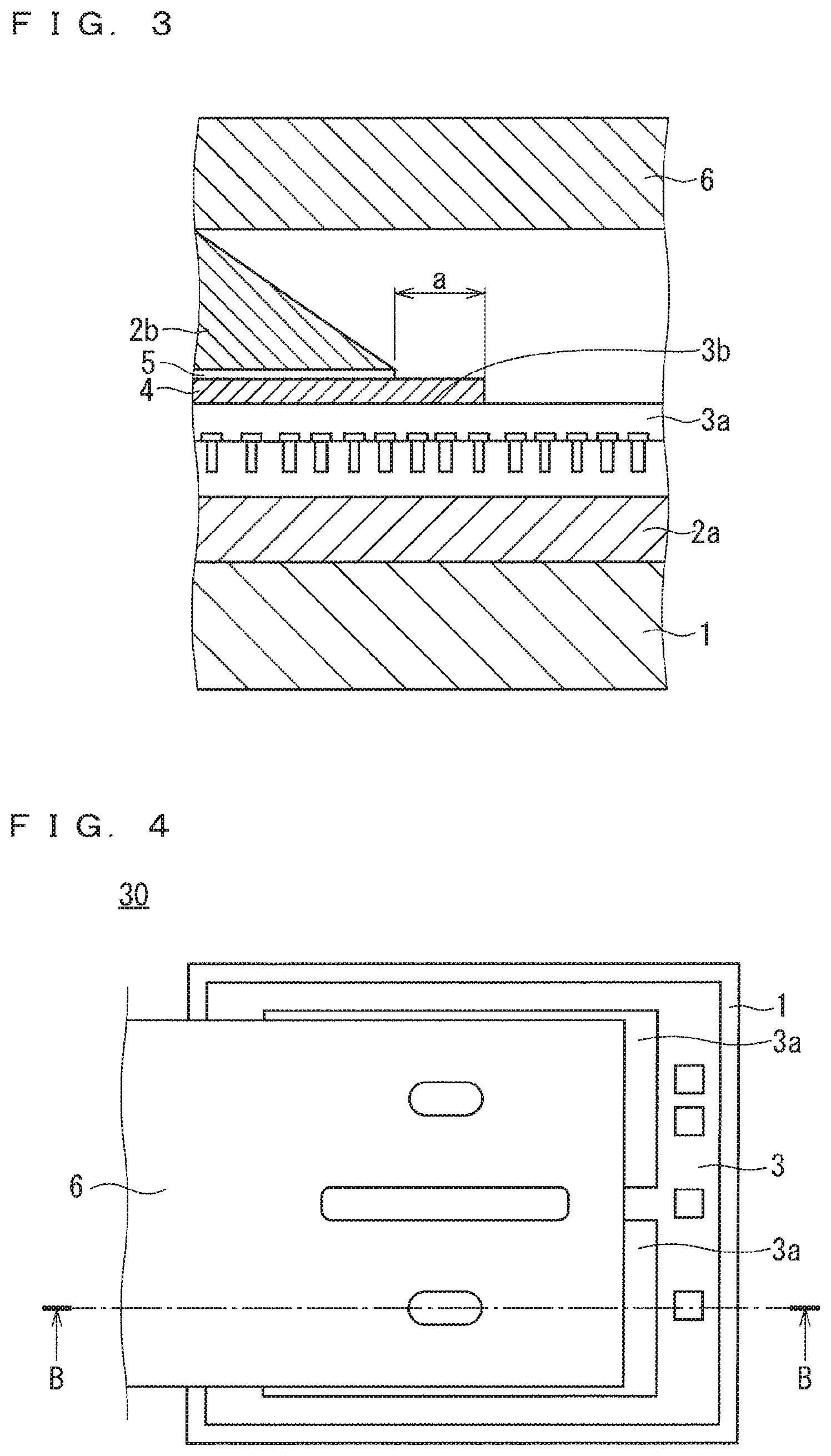
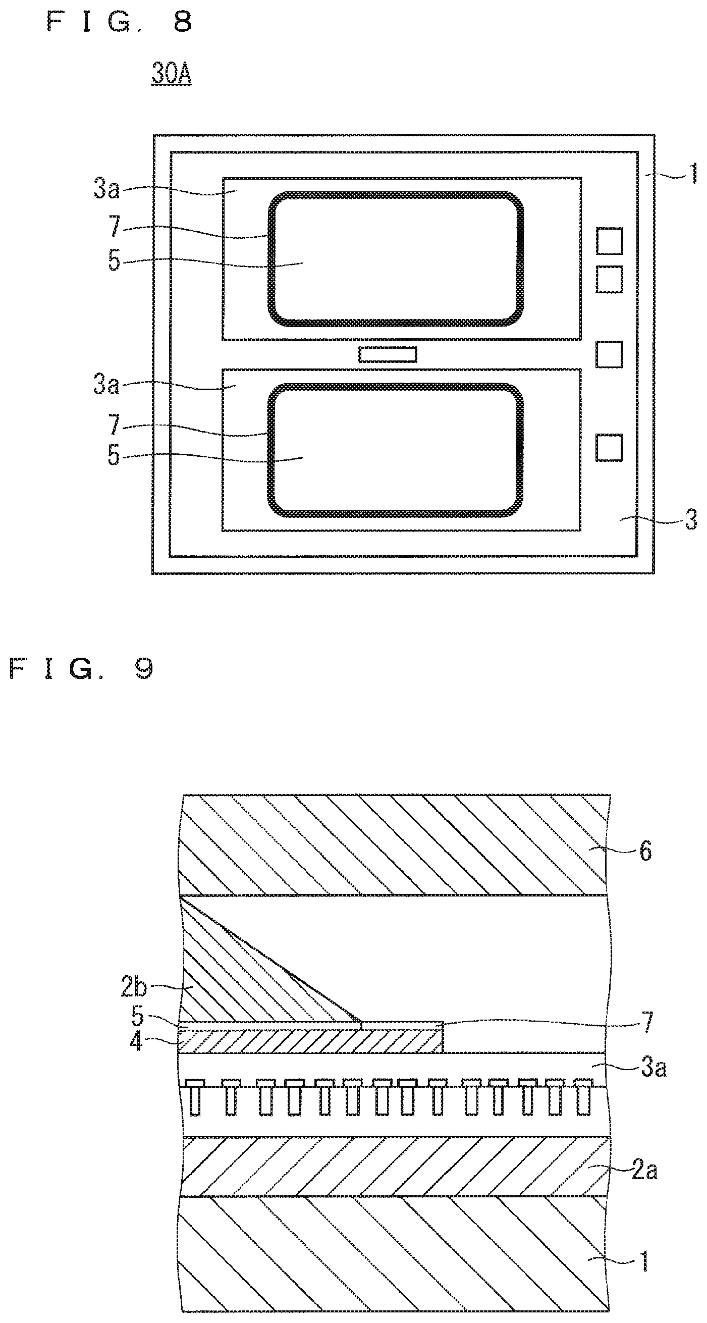
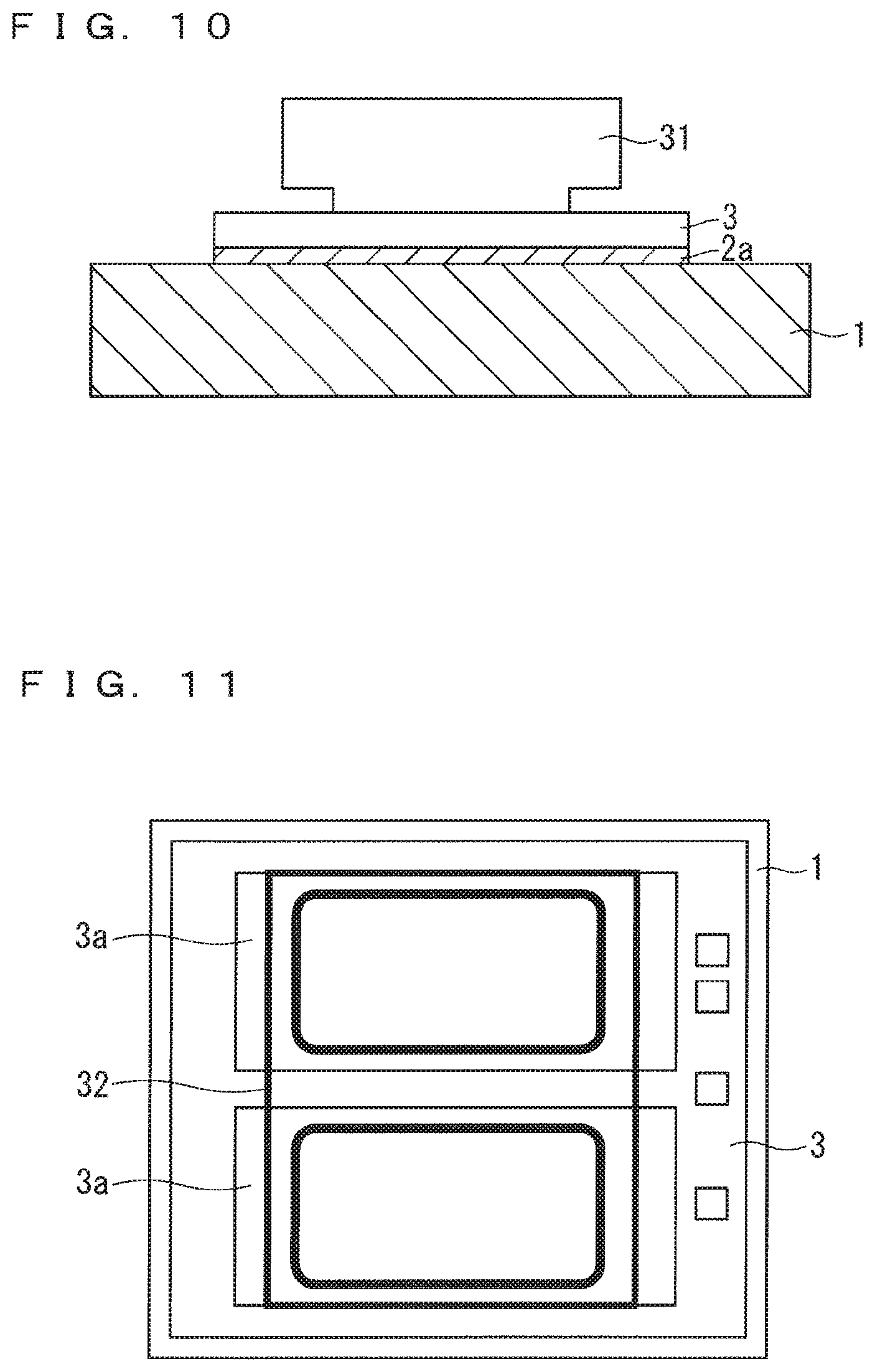
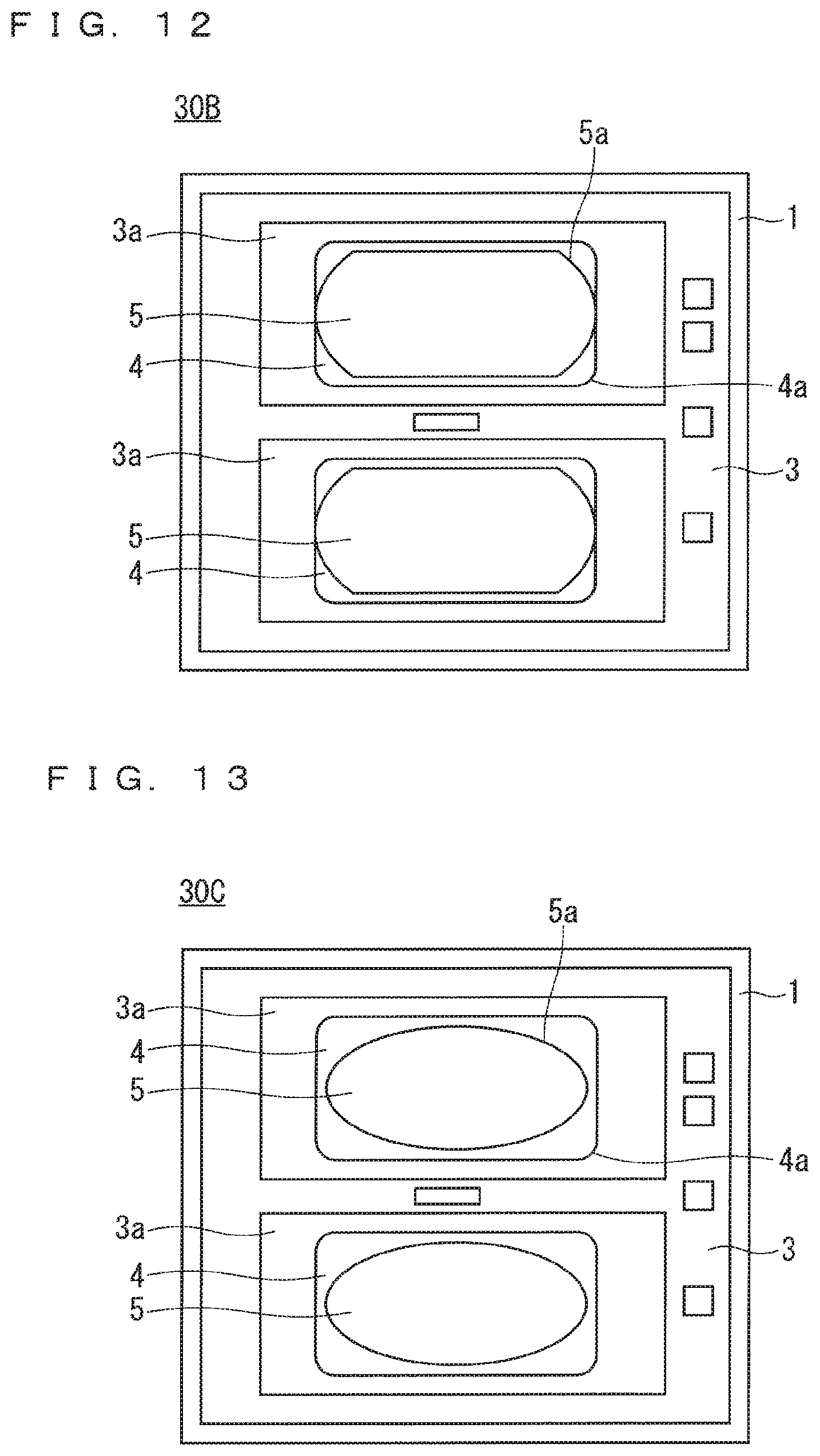
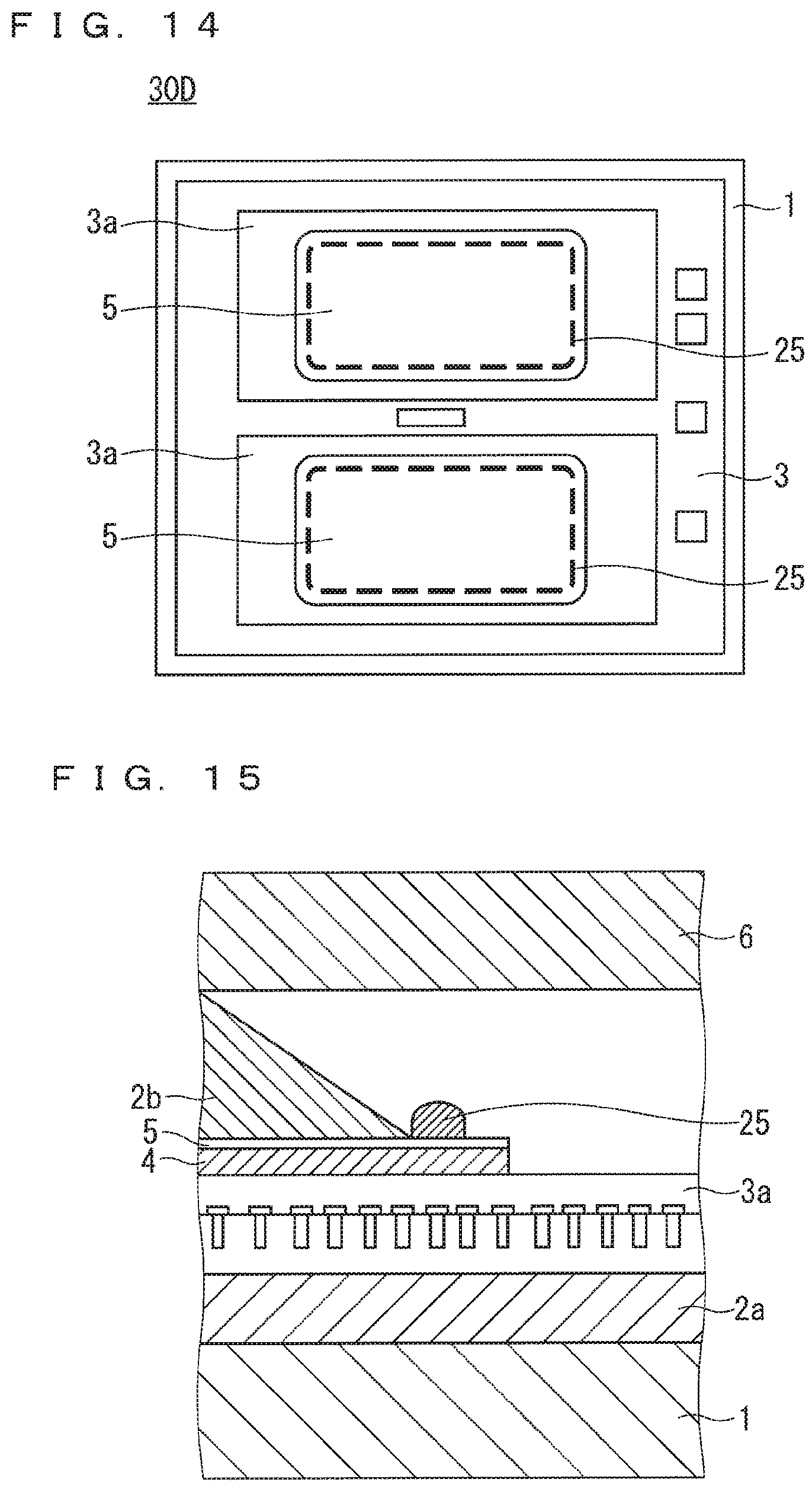
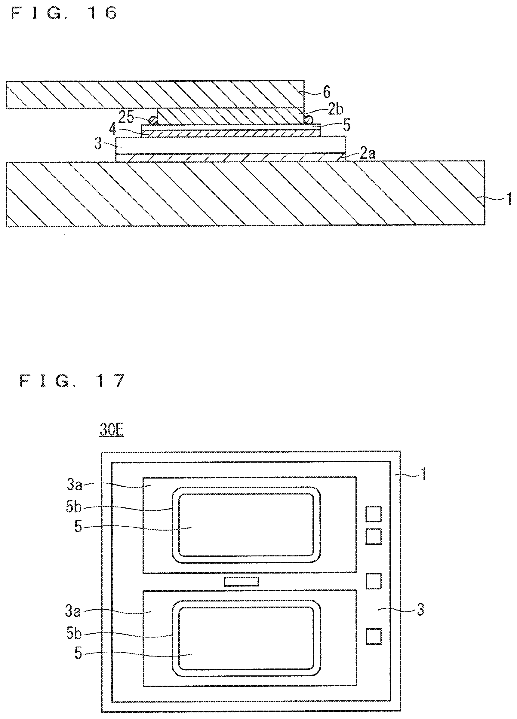
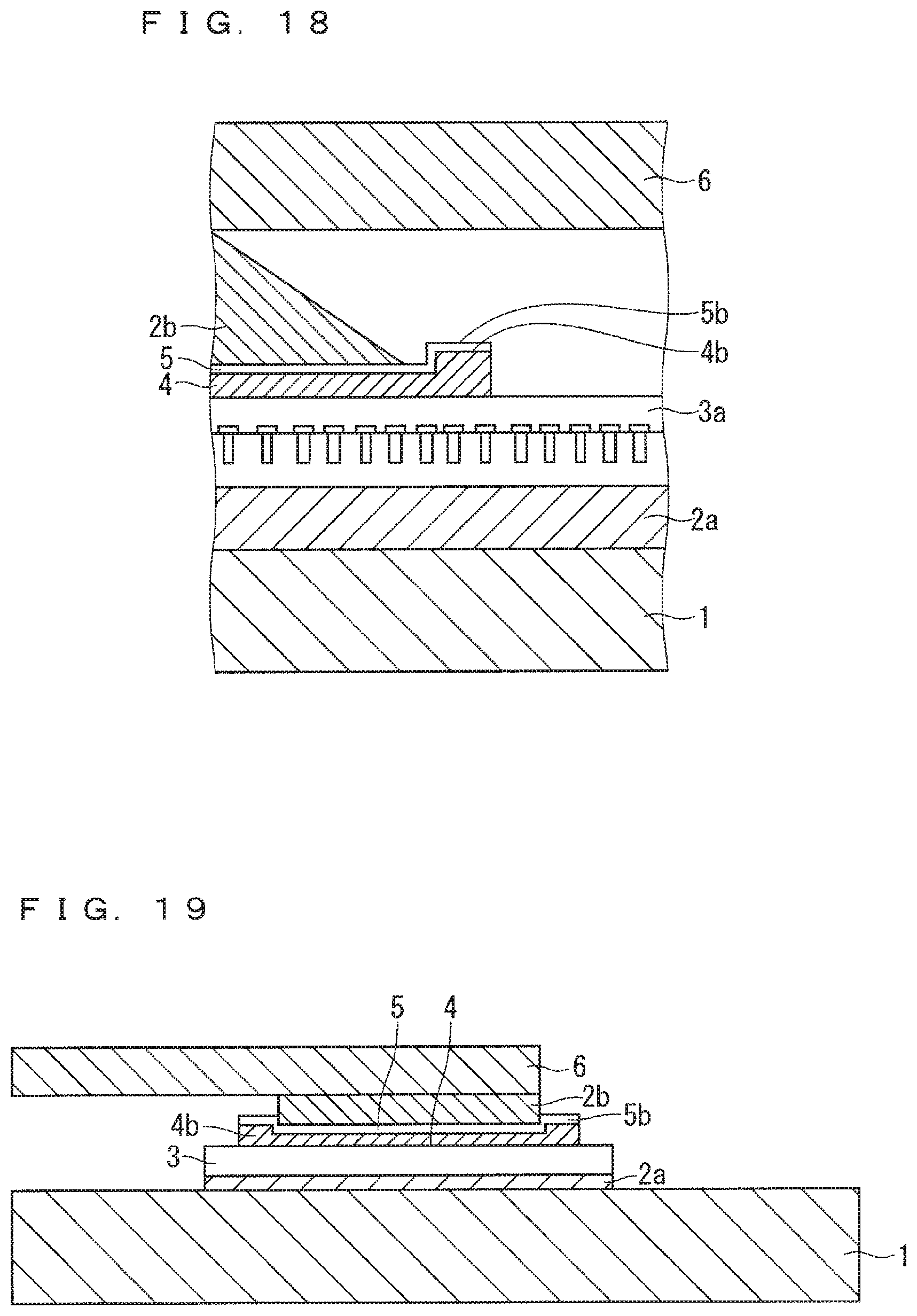
The present invention relates to a structure in which a semiconductor element disposed on a semiconductor device for power control is joined to a lead frame, for instance. A semiconductor device under repeated thermal stress exhibits stress concentration at the peripheral portion of the joint portion between an emitter electrode of a semiconductor element disposed on the semiconductor device, and a lead frame, Such stress concentration damages the emitter electrode. To reduce the stress at the peripheral portion of the joint portion, a coating film has been conventionally formed over the joint portion. Patent Document 1 discloses a thin-film circuit substrate that includes a first metal coating film disposed on a substrate and being highly oxidative, a second metal coating film selectively disposed on the first metal coating film and being highly resistant to oxidation, and an oxidized coating film formed by oxidizing the exposed portions of the first metal coating film. Patent Document 1: Japanese Patent Application Laid-Open No. 7-30242 Unfortunately, to form the coating film over the joint portion between the emitter electrode and the lead frame, required is a changeover to an apparatus that is different from an apparatus for forming a metal film that is formed on a surface of the emitter electrode. In addition, foreign matters can adhere during transfer between process steps. Furthermore, the coating film after formed needs to undergo inspections on position, dimension, thin spots, and other things. Such inspections increase process steps. As with the technique in Patent Document 1, partly removing the thickness of an anti-oxidation film, serving as a solder mask, is a conventionally proposed technique. This technique includes, however, removing part of the anti-oxidation film between adjacent electronic components, and thus fails to reduce the stress generated at the joint portion between the emitter electrode and the lead frame. It is an object of the present invention to provide a technique for reducing process steps, and a stress generated at the peripheral portion of the joint portion between an electrode of a semiconductor element, and a lead frame. A semiconductor device according to the present invention includes the following: a semiconductor element disposed on a heat spreader; a lead frame joined to an electrode of the semiconductor element via a joining material; a metal film disposed on a surface of the electrode; and an anti-oxidation film disposed on a surface of the metal film. The metal film has a peripheral portion that is entirely exposed from the anti-oxidation film. The semiconductor device according to the present invention includes the following: the semiconductor element disposed on the heat spreader; the lead frame joined to the electrode of the semiconductor element via the joining material; the metal film disposed on the surface of the electrode; and the anti-oxidation film disposed on the surface of the metal film. The entire peripheral portion of the metal film is exposed from the anti-oxidation film. The semiconductor device prevents the joining material from flowing and spreading, thereby preventing degradation in the strength of the joint between the electrode and the lead frame. As a result, the electrode of the semiconductor element receives a reduced stress at the peripheral portion of the joint portion between the emitter electrode and the lead frame. In addition, a process step of forming a coating film, which has been conventionally performed, is no longer needed, thereby lowering the possibility that foreign matters can adhere during transfer between process steps. This eliminates the need for inspections, for instance, on the position and dimension of the coating film after formation, and on thin spots in the coating film, thereby reducing process steps. These and other objects, features, aspects and advantages of the present invention will become more apparent from the following detailed description of the present invention when taken in conjunction with the accompanying drawings. The following describes a first embodiment of the present invention with reference to the drawings. First, the power converter 100 according to the first embodiment will be briefly described. The power converter 100 is a power conditioner connected, for instance, between a DC power supply and a power system. This power conditioner converts DC power sent from a photovoltaic cell, a fuel cell, or other things, into AC power, and supplies the AC power to the outside, such as the power system. The power converter 100 includes a main conversion circuit 40 and a control circuit 50. The main conversion circuit 40 includes a semiconductor device 30. The main conversion circuit 40 converts power received from the outside, and outputs the power. The control circuit 50 outputs a control signal for controlling the main conversion circuit 40, to the main conversion circuit 40. Next, the semiconductor device 30 according to the first embodiment will be described. As illustrated in Next, the metal film 4 and the anti-oxidation film 5, both disposed on the surface of the emitter electrode 3 Next, a method for manufacturing the semiconductor device 30 will be described. The semiconductor element 3 is mounted onto the surface of the heat spreader 1 by joining the semiconductor element 3 to the surface via the solder 2 The emitter electrode 3 Referring to the thickness of the stacked films on the surface of the emitter electrode 3 Subsequently, as illustrated in Alternatively, as illustrated in As described above, the semiconductor device 30 according to the first embodiment includes the following: the semiconductor element 3 disposed on the heat spreader 1; the lead frame 6 joined to the emitter electrode 3 The semiconductor device 30 consequently prevents the solder 2 Doing so prevents cracking in the electrode on the surface; such cracking results from the emitter electrode 3 Doing so also eliminates the need for a process step of forming a coating film, which has been conventionally performed, thereby lowering the possibility that foreign matters can adhere during transfer between process steps. This eliminates the need for inspections, for instance, on the position and dimension of the coating film after formation, and on thin spots in the coating film, thereby reducing process steps. The peripheral portion of the metal film 4, which is exposed from the anti-oxidation film 5, is rendered left in the air at room temperature. Accordingly, formed at the peripheral portion of the metal film 4 is a native oxide film. This eliminates the need for covering the outer periphery portion of a surface of a conventional anti-oxidation film, thereby reducing process steps and components. The power converter 100 includes the main conversion circuit 40 having the semiconductor device 30. The conversion circuit 40 converts and then outputs the received power. The power converter 100 also includes the control circuit 50 that outputs the control signal for controlling the main conversion circuit 40, to the main conversion circuit 40. The power converter 100 is consequently highly reliable, and has high quality. The method for manufacturing the semiconductor device 30 includes the following: using the solder plate 12 as the joining material; placing the solder plate 12 onto the surface of the anti-oxidation film 5; and joining the lead frame 6 to the emitter electrode 3 The dimension of the solder plate 12 in plan view is the same as the dimension of the anti-oxidation film 5 in plan view. This forms a solder fillet on the surface of the semiconductor element 3. In addition, changing the size of the solder plate 12 regulates the region for the solder to flow, and regulates the volume of the solder. This improves the assembly performance of the semiconductor device 30. The method for manufacturing the semiconductor device 30 includes the following: using the molten solder 22 as the joining material; putting the molten solder 22 onto the surface of the anti-oxidation film 5; and joining the lead frame 6 to the emitter electrode 3 Accordingly, the molten solder 22 flows and spreads, thus forming a solder fillet on the surface of the semiconductor element 3. The flow and spread of the molten solder 22 regulates the region for the solder to flow. This improves the assembly performance of the semiconductor device 30. The following describes a semiconductor device 30A according to a second embodiment. In the second embodiment, the entire peripheral portion of the metal film 4 is oxidized, as illustrated in The following describes how to form the oxidized portion 7. The anti-oxidation film 5 is formed with the method described in the first embodiment. Subsequently used is a heater 31 having a rectangular shape in plan view for instance, as illustrated in The oxidized portion 7 can be also formed through another process, as illustrated in As described above, the semiconductor device 30A according to the second embodiment, which includes the metal film 4 whose entire peripheral portion is oxidized, further regulates the region for the solder to flow than the semiconductor device according to the first embodiment. This further improves the assembly performance of the semiconductor device 30. As illustrated in As illustrated in Alternatively, the method may include forming a native oxide film at the peripheral portion of the metal film 4 by leaving the peripheral portion of the metal film 4, which is exposed from the anti-oxidation film 5, in the air at room temperature. This alternative method achieves oxidation in a simpler manner than those in The following describes a semiconductor device 30B according to a third embodiment As illustrated in In this case, the anti-oxidation film 5 may be circular or elliptical in plan view, as illustrated in As described above, the semiconductor device 30B according to the third preferred embodiment includes the anti-oxidation film 5 having the corner portion 5 The following describes a semiconductor device 30D according to a fourth embodiment. As illustrated in The wire 25 is made of the same material as the signal wire. This allows the wire 25 to be placed at the time of conventional wire bonding and to be placed using the same equipment, thereby eliminating the need for a changeover. It is noted that the wire 25 may be an aluminum wire having a diameter Φ of 50 μm or greater and 500 μm or less, and may undergo bonding in stitch form. Alternatively, the wire 25 may be a single long wire, and the single long wire 25 may be continuously disposed throughout the peripheral portion of the anti-oxidation film 5. As described above, the semiconductor device 30D according to the fourth embodiment includes the metal wires 25 disposed throughout the peripheral portion of the anti-oxidation film 5. The metal wires 25 prevent the solder 2 Doing so prevents cracking in the electrode on the surface; such cracking results from the emitter electrode 3 Doing so also eliminates the need for a process step of forming a coating film, which has been conventionally performed, thereby lowering the possibility that foreign matters can adhere during transfer between process steps. This eliminates the need for inspections, for instance, on the position and dimension of the coating film after formation, and on thin spots in the coating film, thereby reducing process steps. The wire 25 is made of the same material as the signal wire. This allows the wire 25 to be placed at the time of conventional wire bonding and to be placed using the same equipment, thereby eliminating the need for a changeover. The following describes a semiconductor device 30E according to a fifth embodiment. As illustrated in The following briefly describes how to form the step portion 4 As described above, the semiconductor device 30E according to the fifth embodiment includes the anti-oxidation film 5 that has the step portion 5 The step portions 5 Doing so prevents cracking in the electrode on the surface; such cracking results from the emitter electrode 3 Doing so also eliminates the need for a process step of forming a coating film, which has been conventionally performed, thereby lowering the possibility that foreign matters can adhere during transfer between process steps. This eliminates the need for inspections, for instance, on the position and dimension of the coating film after formation, and on thin spots in the coating film, thereby reducing process steps. While the invention has been shown and described in detail, the foregoing description is in all aspects illustrative and not restrictive. It is therefore understood that numerous modifications and variations can be devised without departing from the scope of the invention. It is noted that in the present invention, the individual embodiments can be freely combined, or can be modified and omitted as appropriate, within the scope of the invention. 1 heat spreader, 2 An object is to provide a technique for reducing process steps, and a stress generated at the peripheral portion of the joint portion between an electrode of a semiconductor element and a lead frame. A semiconductor device includes the following: a semiconductor element disposed on a heat spreader; a lead frame joined to an emitter electrode of the semiconductor element via solder, which is a joining material; a metal film disposed on a surface of the emitter electrode; and an anti-oxidation film disposed on a surface of the metal film. The metal film has a peripheral portion that is entirely exposed from the anti-oxidation film. 1. A semiconductor device comprising:
a semiconductor element disposed on a heat spreader; a lead frame joined to an electrode of the semiconductor element via a joining material; a metal film disposed on a surface of the electrode; and an anti-oxidation film disposed on a surface of the metal film, wherein the metal film comprises a peripheral portion that is entirely exposed from the anti-oxidation film. 2. The semiconductor device according to 3. The semiconductor device according to 4. The semiconductor device according to 5. A semiconductor device comprising:
a semiconductor element disposed on a heat spreader; a lead frame joined to an electrode of the semiconductor element via a joining material; a metal film disposed on a surface of the electrode; an anti-oxidation film disposed on a surface of the metal film; and a metal wire disposed throughout a peripheral portion of the anti-oxidation film. 6. A semiconductor device comprising:
a semiconductor element disposed on a heat spreader; a lead frame joined to an electrode of the semiconductor element via a joining material; a metal film disposed on a surface of the electrode; an anti-oxidation film disposed on a surface of the metal film; and step portions disposed throughout peripheral portions of the anti-oxidation film and the metal film, the step portions protruding upward. 7. A power converter comprising:
a main conversion circuit comprising the semiconductor device according to a control circuit configured to output a control signal for controlling the main conversion circuit, to the main conversion circuit. 8. A method for manufacturing the semiconductor device according to using a solder plate as the joining material; placing the solder plate onto a surface of the anti-oxidation film; and joining the lead frame to the electrode using the solder plate. 9. A method for manufacturing the semiconductor device according to using molten solder as the joining material; putting the molten solder onto a surface of the anti-oxidation film; and joining the lead frame to the electrode using the molten solder. 10. A method for manufacturing the semiconductor device according to oxidizing a contact portion of the metal film by moving a heater through the entire peripheral portion of the metal film, with the heater brought into contact with the peripheral portion. 11. A method for manufacturing the semiconductor device according to oxidizing a contact portion of the metal film while bringing a heater having a frame shape into contact with the entire peripheral portion of the metal film at the same time. 12. A power converter comprising:
a main conversion circuit comprising the semiconductor device according to a control circuit configured to output a control signal for controlling the main conversion circuit, to the main conversion circuit. 13. A power converter comprising:
a main conversion circuit comprising the semiconductor device according to a control circuit configured to output a control signal for controlling the main conversion circuit, to the main conversion circuit.TECHNICAL FIELD
BACKGROUND ART
PRIOR ART DOCUMENT
Patent Document
SUMMARY
Problem to be Solved by the Invention
Means to Solve the Problem
Effects of the Invention
BRIEF DESCRIPTION OF DRAWINGS
DESCRIPTION OF EMBODIMENT(S)
First Embodiment
Second Embodiment
Third Embodiment
Fourth Embodiment
Fifth Embodiment
EXPLANATION OF REFERENCE SIGNS