Hybrid Bonding Systems and Methods for Semiconductor Wafers
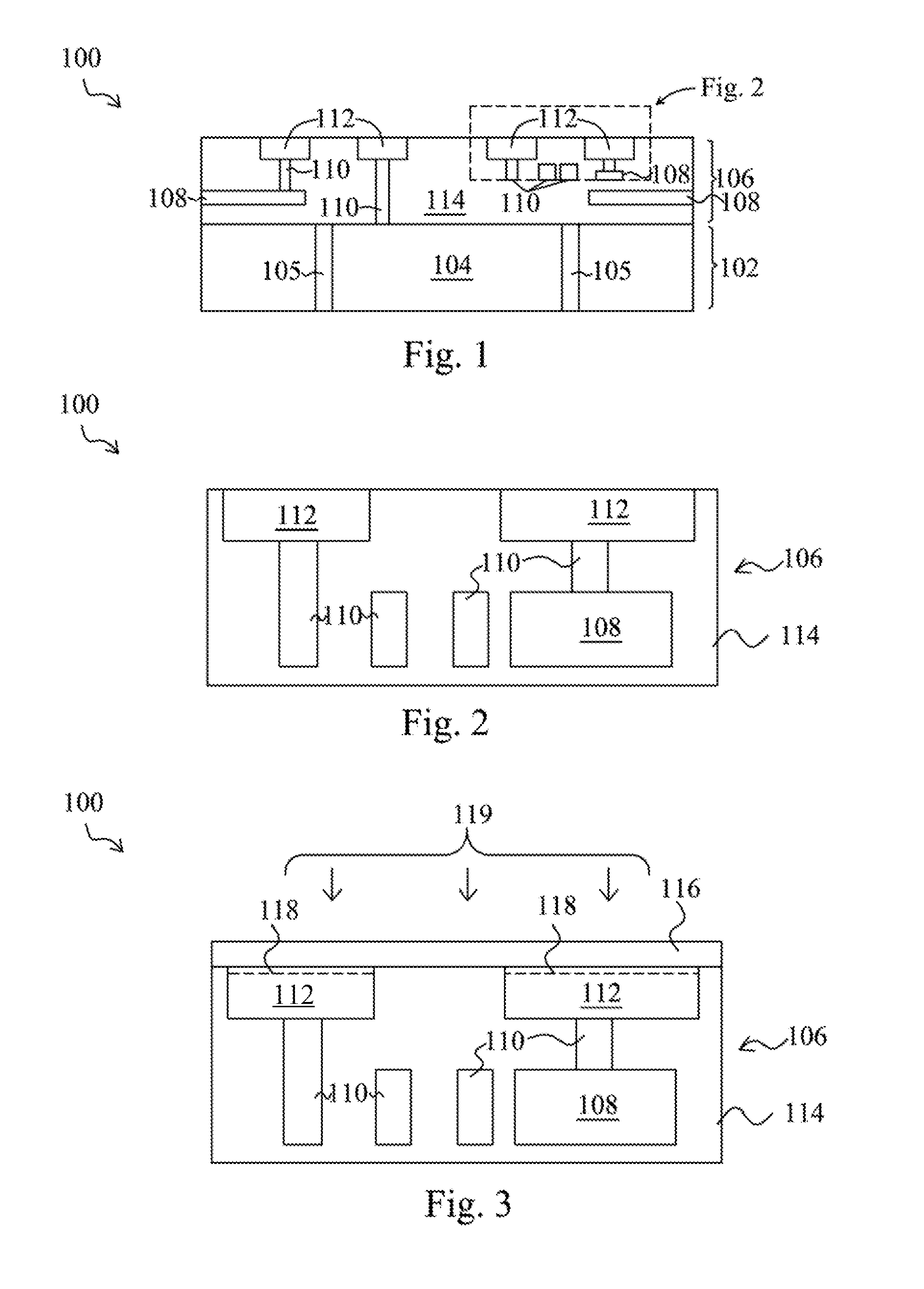
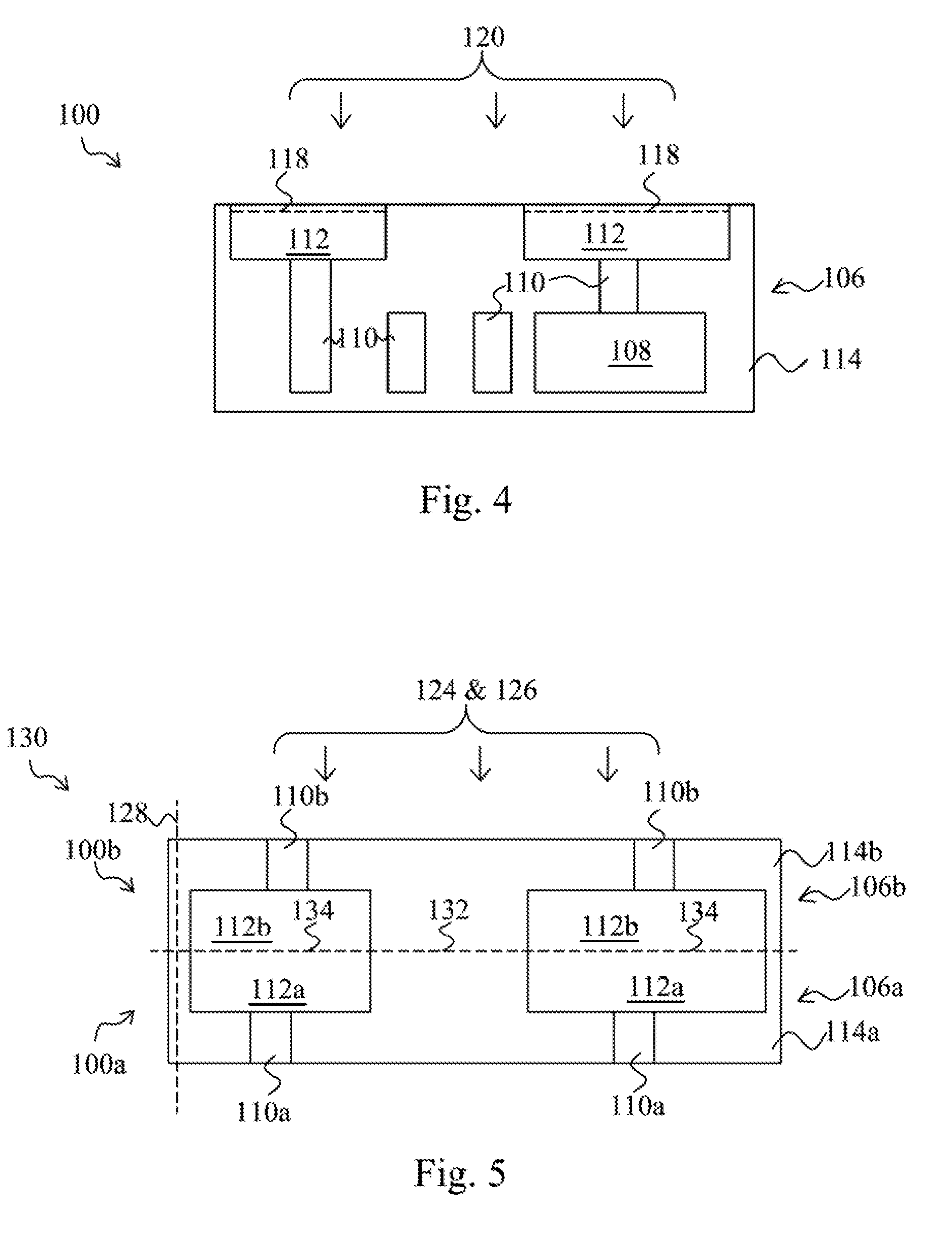
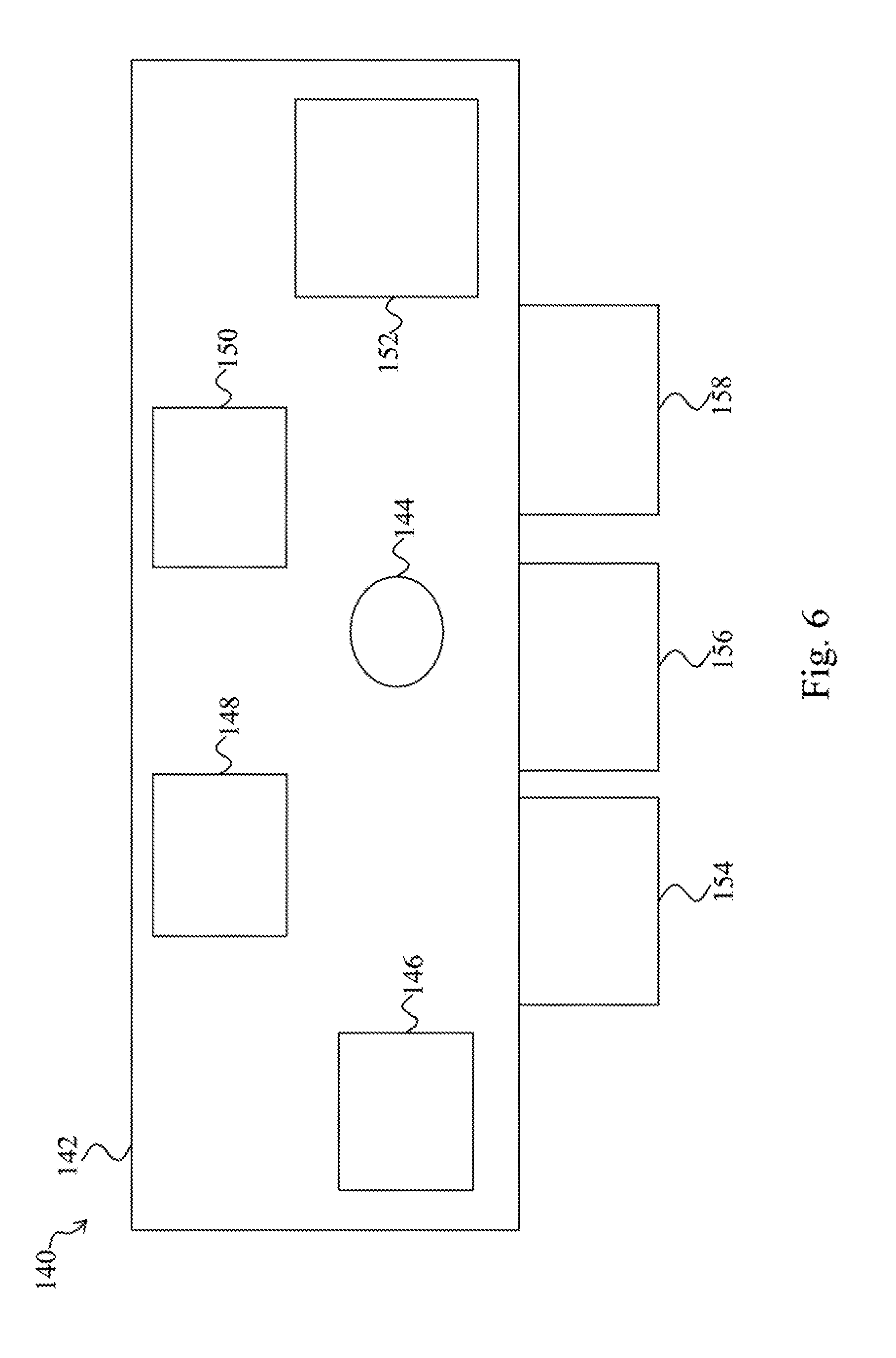
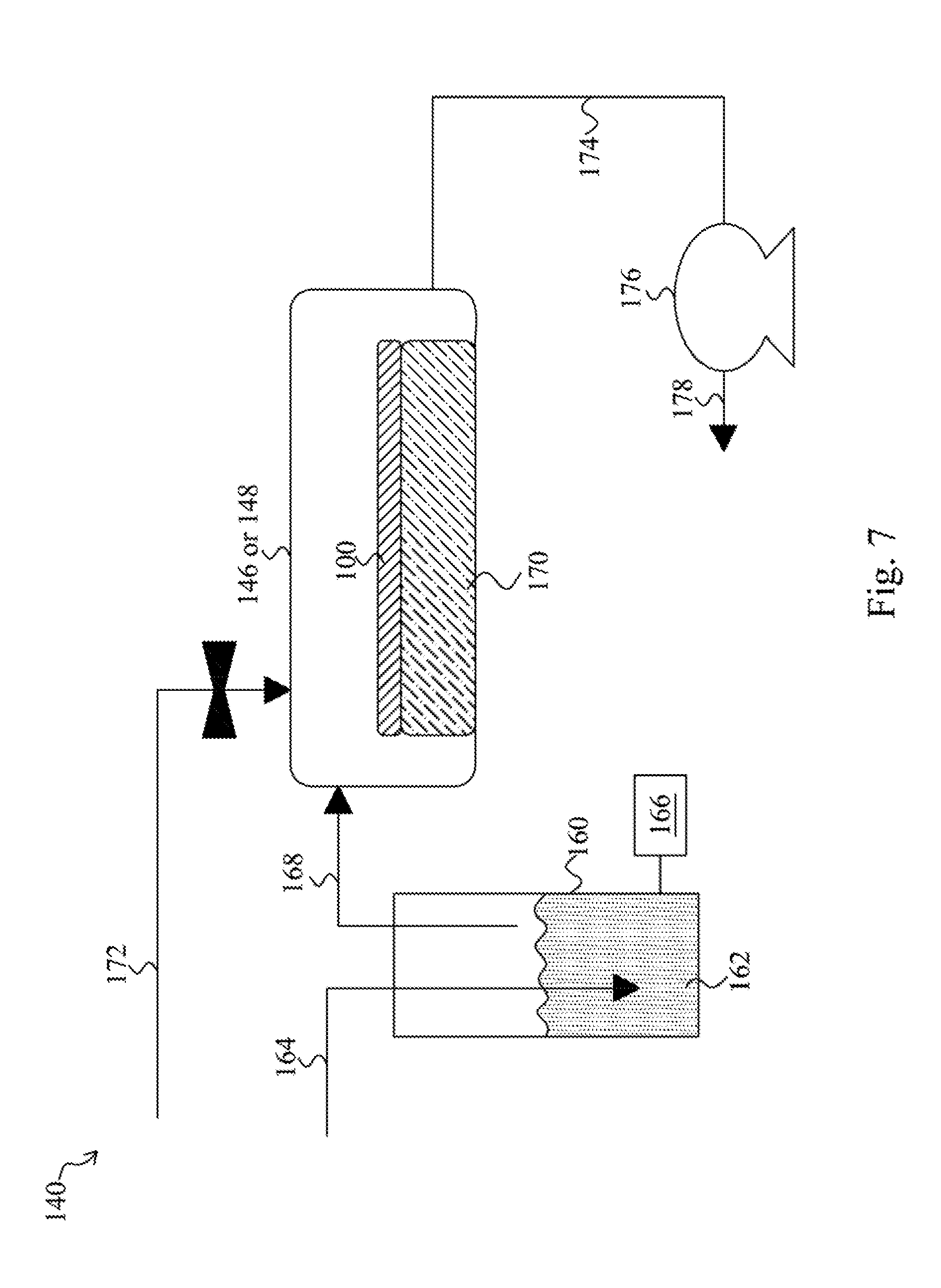
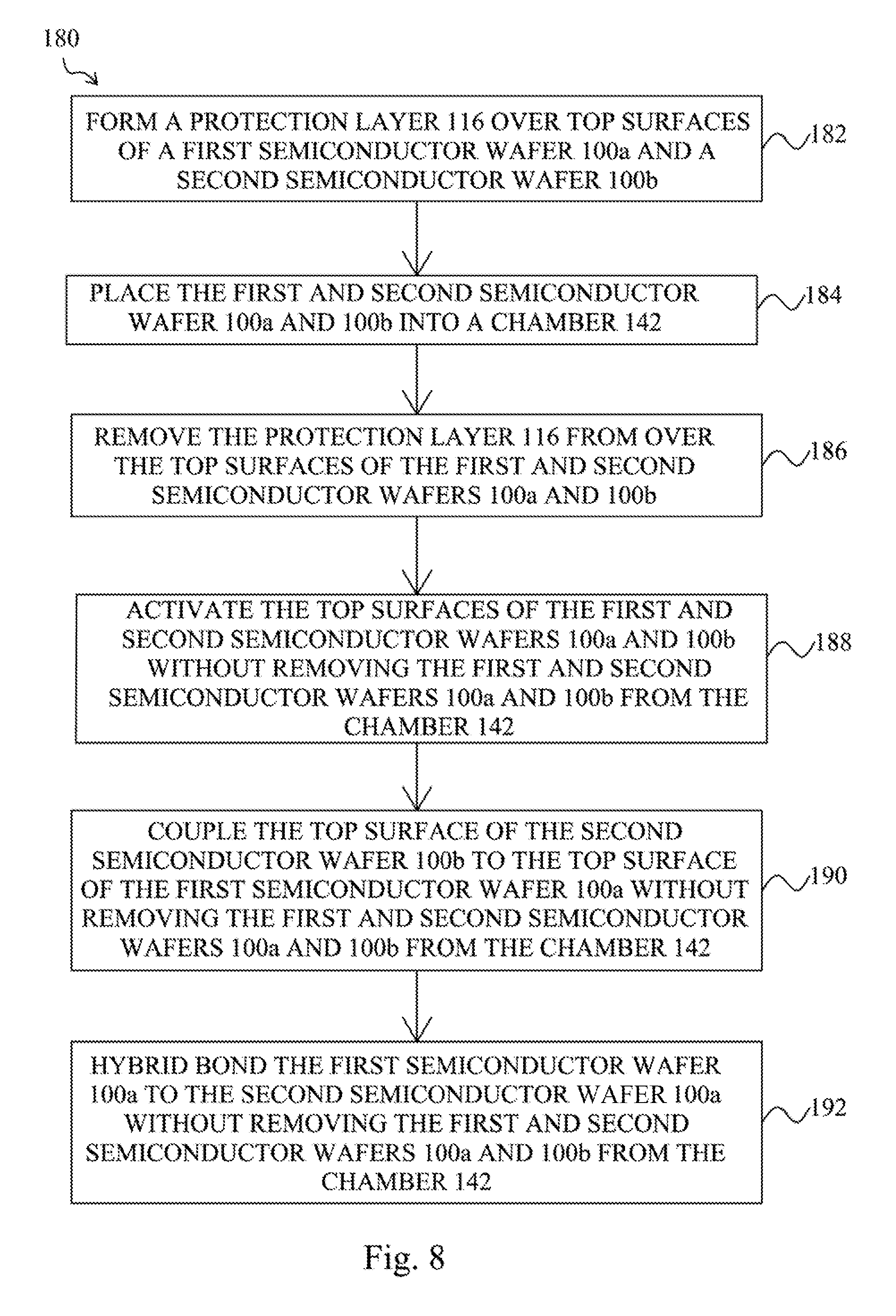
This application is a continuation of U.S. application Ser. No. 15/689,982, filed on Aug. 29, 2017, which is a continuation of U.S. application Ser. No. 14/725,266, filed May 29, 2015, now U.S. Pat. No. 9,748,198 issued Aug. 29, 2017, which is a continuation of U.S. application Ser. No. 13/542,507, filed on Jul. 5, 2012, now U.S. Pat. No. 9,048,283 filed Jun. 2, 2015, which applications are hereby incorporated herein by reference. This application relates to the following co-pending and commonly assigned patent application: Ser. No. 13/488,745, filed on Jun. 5, 2012, entitled, “Three Dimensional Integrated Circuit Structures and Hybrid Bonding Methods for Semiconductor Wafers,” which application is hereby incorporated herein by reference. Semiconductor devices are used in a variety of electronic applications, such as personal computers, cell phones, digital cameras, and other electronic equipment, as examples. Semiconductor devices are typically fabricated by sequentially depositing insulating or dielectric layers, conductive layers, and semiconductive layers of material over a semiconductor substrate, and patterning the various material layers using lithography to form circuit components and elements thereon. Dozens or hundreds of integrated circuits are typically manufactured on a single semiconductor wafer, and individual dies on the wafer are singulated by sawing between the integrated circuits along a scribe line. The individual dies are typically packaged separately, in multi-chip modules, or in other types of packaging, for example. The semiconductor industry continues to improve the integration density of various electronic components (e.g., transistors, diodes, resistors, capacitors, etc.) by continual reductions in minimum feature size, which allow more components to be integrated into a given area. These smaller electronic components also require smaller packages that utilize less area than packages of the past, in some applications. Three dimensional integrated circuits (3DICs) are a recent development in semiconductor packaging in which multiple semiconductor dies are stacked upon one another, such as package-on-package (PoP) and system-in-package (SiP) packaging techniques. 3DICs provide improved integration density and other advantages, such as faster speeds and higher bandwidth, because of the decreased length of interconnects between the stacked dies, as examples. Hybrid bonding is one type of bonding procedure for 3DICs, wherein two semiconductor wafers are bonded together using a hybrid bonding technique. Some methods of forming 3DICs are described in patent application: Ser. No. 13/488,745, filed on Jun. 5, 2012, entitled, “Three Dimensional Integrated Circuit Structures and Hybrid Bonding Methods for Semiconductor Wafers,” which application is hereby incorporated herein by reference. For a more complete understanding of the present disclosure, and the advantages thereof, reference is now made to the following descriptions taken in conjunction with the accompanying drawings, in which: Corresponding numerals and symbols in the different figures generally refer to corresponding parts unless otherwise indicated. The figures are drawn to clearly illustrate the relevant aspects of the embodiments and are not necessarily drawn to scale. The making and using of the embodiments of the present disclosure are discussed in detail below. It should be appreciated, however, that the present disclosure provides many applicable inventive concepts that can be embodied in a wide variety of specific contexts. The specific embodiments discussed are merely illustrative of specific ways to make and use the disclosure, and do not limit the scope of the disclosure. Embodiments of the present disclosure are related to 3DIC packaging of semiconductor devices. Novel hybrid bonding systems and method for semiconductor wafers will be described herein. Referring first to The semiconductor wafer 100 includes a workpiece 102. The workpiece 102 includes a semiconductor substrate comprising silicon or other semiconductor materials and may be covered by an insulating layer, for example. The workpiece 102 may comprise silicon oxide over single-crystal silicon, for example. Compound semiconductors, GaAs, InP, Si/Ge, or SiC, as examples, may be used in place of silicon. The workpiece 102 may comprise a silicon-on-insulator (SOI) or a germanium-on-insulator (GOI) substrate, as examples. The workpiece 102 may include a device region 104 formed proximate a top surface of the workpiece 102. The device region 104 includes active components or circuits, such as conductive features, implantation regions, resistors, capacitors and other semiconductor elements, e.g., transistors, diodes, etc. The device region 104 is formed over the workpiece 102 in a front-end-of-line (FEOL) process in some embodiments, for example. The workpiece 102 may also include through-substrate vias (TSVs) 105 comprising a conductive material that provide connections from a bottom side to a top side of the workpiece 102, as shown. A metallization structure 106 is formed over the workpiece 102, e.g., over the device region 104 of the workpiece 102. The metallization structure 106 is formed over the workpiece 102 in a back-end-of-line (BEOL) process in some embodiments, for example. The metallization structure 106 includes conductive features, such as conductive lines 108, vias 110, and conductive pads 112 formed in an insulating material 114. The conductive pads 112 comprise contact pads or bond pads formed on a top surface of the semiconductor wafer 100, as examples. Some of the vias 110 couple conductive pads 112 to conductive lines 108 in the metallization structure 106, and other vias 110 couple contact pads 112 to the device region 104 of the workpiece 102. Vias 110 may also connect together conductive lines 108 in different metallization layers, not shown. The conductive features may comprise conductive materials typically used in BEOL processes, such as Cu, Al, W, Ti, TiN, Ta, TaN, or multiple layers or combinations thereof. In accordance with an embodiment, the conductive pads 112 disposed proximate a top surface of the metallization structure 106 comprise Cu or a copper alloy, for example. The metallization structure 106 shown is merely for illustrative purposes: the metallization structure 106 may comprise other configurations and may include one or more conductive line and via layers, for example. Some semiconductor wafers 100 may have three conductive line and via layers, or four or more conductive line and via layers, as other examples. The semiconductor wafer 100 includes a plurality of semiconductor devices comprising portions of the workpiece 102 and the metallization layer 106 formed across the surface thereof, e.g., in a grid. The semiconductor devices comprise dies that may each be shaped in a square or rectangular pattern in a top view of the workpiece 102, as examples. The conductive pads 112 are formed in some embodiments using a damascene process, wherein the insulating material 114 is deposited over the workpiece 102, and the insulating material 114 is patterned using lithography. The patterned insulating material 114 is filled with a conductive material, and excess portions of the conductive material are removed from over the top surface of the insulating material 114 using a chemical mechanical polishing (CMP) process, an etch process, or combinations thereof. In other embodiments, a conductive material may be deposited and patterned using lithography, and the insulating material 114 is formed over the conductive material to form the conductive pads 112 using a subtractive etch process. The excess insulating material 114 is then removed from over the conductive pads 112 using a CMP process, an etch process, or combinations thereof. In accordance with some embodiments of the present disclosure, after the formation of the conductive pads 112, a CMP process is performed near an end of the fabrication process of the semiconductor wafer 100. After the conductive pads 112 are formed and cleaned, a protection layer 116 is formed over the top surface of the semiconductor wafer 100, as shown in The protection layer 116 is formed in some embodiments using a vapor type deposition process or a hydrophobic process having a contact angle of greater than about 60 degrees to the top surface of the semiconductor wafer 100. Alternatively, the protection layer 116 may be formed using other methods. The protection layer 116 comprises a thickness of about 100 Angstroms or less. Alternatively, the protection layer 116 may comprise other dimensions. In some embodiments, the protection layer 116 comprises a monolayer of material. The semiconductor wafer 100 is then stored for a period of time in some embodiments. The semiconductor wafer 100 may be placed in a fabrication facility in storage or on a shelf for a period of time after the manufacturing process is completed, for example. Advantageously, the amount of time that the semiconductor wafer 100 may be stored is increased, due to the presence of the protection layer 116, which prevents or relaxes the formation of an oxide material on the top surfaces of the conductive pads 112. The protection layer 116 prevents the formation of Cu oxide on top surfaces of the conductive pads 112, in embodiments where the conductive pads 112 comprise Cu or Cu alloys, for example. When it is time for the semiconductor wafer 100 to be packaged using a 3DIC process with another semiconductor wafer 100, the wafer 100 is placed into a chamber 142 (not shown in Before the protection layer 116 is formed, an oxide material 118 may begin forming soon after a final fabrication step on top surfaces of the conductive pads 112, depending on the manufacturing environment, for example, because Cu oxidizes easily. The oxide material 118 may comprise copper oxide (CuOx) for example, by exposure of the Cu conductive pads 112 to oxygen in the ambient air. The oxide material 118 may comprise other materials, depending on the type of material of the conductive pads 112, for example. Removal of the oxide material 118 from the top surfaces of the conductive pads 112 is important to achieve a high quality hybrid bond to another semiconductor wafer 100, to avoid high resistance connections between the wafers 100. Advantageously, in some embodiments, a portion of or all of the oxide material 118 is removed during the removal process 119 used to remove the protection layer 116 from the top surface of the wafer 100. The removal process 119 may also clean the top surface of the wafer 100, in some embodiments. The removal process 119 of the protection layer 116 is performed without removing the wafer 100 from the chamber 142, to avoid forming any additional oxide material 118 on the top surface of the conductive pads 112. Next, the top surface of the wafer 100 is activated using an activation process 120, as shown in After the activation process 120, the wafers 100 may be cleaned in some embodiments. The cleaning process may comprise exposure to deionized (DI) H2O, exposure to NH4OH, exposure to diluted hydrofluoric acid (DHF) (e.g., at a concentration of less than about 1% HF acid), exposure to other acids, a cleaning process with a brush, a mega-sonic procedure, a spin process, exposure to an infrared (IR) lamp, or a combination thereof, as examples, although alternatively, the cleaning process may comprise other types of cleaning processes. The cleaning process enhances a density of a hydroxy group disposed on top surfaces of the wafer 100 in some embodiments, e.g., on the top surface of the conductive pads 112. Enhancing the density of the hydroxy group on the conductive pads 112 advantageously increases bonding strength and reduces the anneal temperature required for the hybrid bonding process, for example. The cleaning process is performed without removing the wafer 100 from the chamber 142, again, to avoid forming any additional oxide material 118 on the top surface of the conductive pads 112. The removal process 119, the activation process 120 and the cleaning process are adapted to prepare the top surface of the wafer 100 for hybrid bonding to another wafer 100, for example, so that the top surfaces of the wafers 100 are as clean as possible so that a high quality hybrid bond is formed between two or more wafers 100. The removal process 119, the activation process 120, and the cleaning process assist in the hybrid bonding of two or more wafers 100, advantageously allowing the use of lower pressures and temperatures in a subsequent hybrid bonding process. The removal process 119, the activation process 120 and/or the cleaning process may be used to remove a portion of or all of the oxide material 118. A consideration of a selection of chemistries for portions of the removal process 119, the activation process 120 and/or the cleaning process may include the following reactions, to reduce an oxide material 118 comprising CuOx, as an example: After the cleaning process, next, without removing the wafer 100 from the chamber 142, the wafer 100 shown in The bonding of the second semiconductor wafer 100 After the alignment process of the wafers 100 The hybrid bonding process results in a bond 132 that is formed between the insulating materials 114 The resulting 3DIC structure 130 shown in Port 154 comprises a first load port that is adapted to support a plurality of the first semiconductor wafers 100 Next, or sequentially and simultaneously with the processing of the first semiconductor wafer 100 The protection layer 116 is removed in a separate sub-chamber 146, the top surface of the wafers 100, 100 The hybrid bonding system 140 advantageously comprises a single platform wherein a plurality of wafers 100 Three or more semiconductor wafers 100, 100 One or more semiconductor devices on the second semiconductor wafer 100 Embodiments of the present disclosure include methods of hybrid bonding semiconductor wafers to form 3DIC structures 130, and also include systems 140 adapted to perform the methods of hybrid bonding described herein. In some embodiments, the plurality of conductive pads of the first semiconductor wafer and the second semiconductor wafer comprise Cu, and the insulating materials of the first semiconductor wafer and the second semiconductor wafer comprise SiO2, wherein the hybrid bonding methods described herein comprise a Cu/SiO2wafer level hybrid bonding process. Advantages of embodiments of the disclosure include providing novel hybrid bonding methods and systems 140 that provide high quality hybrid bonds for 3DICs. The innovating methods and systems 140 provide the ability to remove protection layers 116 and reduce the formation of oxide material 118 on conductive pads 112 in a hybrid bond procedure in a single platform. Integrating the hybrid bonding process into a single platform reduces cost of ownership (CoO). The protection layer 116 insulates the conductive pad 112 surface and also prevents or relaxes oxide material 118 formation. The protection layer 116 provides the ability to increase a storage time (Q), comprising a time period between forming the protection layer 116 and hybrid bonding wafers 100 together. A Q of greater than about 1 day (e.g., weeks or months or more) is advantageously achievable by embodiments of the present disclosure, for example; thus, a concern of shortening Q time is eliminated in the hybrid bonding procedure. The novel hybrid bonding methods and systems 140 lower contact resistance of the bonds of the conductive pads 112 A high accuracy in alignment of the wafers 100 In accordance with one embodiment of the present disclosure, a hybrid bonding system for semiconductor wafers includes a chamber and a plurality of sub-chambers disposed within the chamber. A robotics handler is disposed within the chamber that is adapted to move a plurality of semiconductor wafers within the chamber between the plurality of sub-chambers. The plurality of sub-chambers includes a first sub-chamber adapted to remove a protection layer from the plurality of semiconductor wafers, and a second sub-chamber adapted to activate top surfaces of the plurality of semiconductor wafers prior to hybrid bonding the plurality of semiconductor wafers together. The plurality of sub-chambers also includes a third sub-chamber adapted to align the plurality of semiconductor wafers and hybrid bond the plurality of semiconductor wafers together. In accordance with another embodiment, a hybrid bonding method for semiconductor wafers includes forming a protection layer over top surfaces of a first semiconductor wafer and a second semiconductor wafer, and placing the first semiconductor wafer and the second semiconductor wafer into a chamber. The protection layer is removed from over the top surfaces of the first semiconductor wafer and the second semiconductor wafer, and the top surfaces of the first semiconductor wafer and the second semiconductor wafer are activated. The method includes coupling the top surface of the second semiconductor wafer to the top surface of the first semiconductor wafer, and hybrid bonding the first semiconductor wafer to the second semiconductor wafer. Removing the protection layer, activating the top surfaces, coupling the top surface of the second semiconductor wafer to the top surface of the first semiconductor wafer, and hybrid bonding the first semiconductor wafer to the second semiconductor wafer are performed without removing the first semiconductor wafer and the second semiconductor wafer from the chamber. In accordance with yet another embodiment, a hybrid bonding method for semiconductor wafers includes providing a first semiconductor wafer and a second semiconductor wafer, the first semiconductor wafer and the second semiconductor wafer each having a plurality of conductive pads disposed within an insulating material on a top surface thereof. A protection layer is formed over the top surfaces of the first semiconductor wafer and the second semiconductor wafer, and the first semiconductor wafer and the second semiconductor wafer are placed into a chamber. The protection layer is removed from over the top surfaces of the first semiconductor wafer and the second semiconductor wafer, and the top surfaces of the first semiconductor wafer and the second semiconductor wafer are activated. The top surfaces of the first semiconductor wafer and the second semiconductor wafer are cleaned, and the top surfaces of the second semiconductor wafer and the first semiconductor wafer are coupled together. The first semiconductor wafer is hybrid bonded to the second semiconductor wafer. Hybrid bonding the first semiconductor wafer to the second semiconductor wafer includes forming a first bond between the insulating material of the first semiconductor wafer and the insulating material of the second semiconductor wafer and forming a second bond between the plurality of conductive pads of the first semiconductor wafer and the plurality of conductive pads of the second semiconductor wafer. Removing the protection layer, activating the top surfaces, cleaning the top surfaces, coupling together the top surfaces, and hybrid bonding the first semiconductor wafer to the second semiconductor wafer are performed without removing the first semiconductor wafer and the second semiconductor wafer from the chamber. Although embodiments of the present disclosure and their advantages have been described in detail, it should be understood that various changes, substitutions and alterations can be made herein without departing from the spirit and scope of the disclosure as defined by the appended claims. For example, it will be readily understood by those skilled in the art that many of the features, functions, processes, and materials described herein may be varied while remaining within the scope of the present disclosure. Moreover, the scope of the present application is not intended to be limited to the particular embodiments of the process, machine, manufacture, composition of matter, means, methods and steps described in the specification. As one of ordinary skill in the art will readily appreciate from the disclosure of the present disclosure, processes, machines, manufacture, compositions of matter, means, methods, or steps, presently existing or later to be developed, that perform substantially the same function or achieve substantially the same result as the corresponding embodiments described herein may be utilized according to the present disclosure. Accordingly, the appended claims are intended to include within their scope such processes, machines, manufacture, compositions of matter, means, methods, or steps. Hybrid bonding systems and methods for semiconductor wafers are disclosed. In one embodiment, a hybrid bonding system for semiconductor wafers includes a chamber and a plurality of sub-chambers disposed within the chamber. A robotics handler is disposed within the chamber that is adapted to move a plurality of semiconductor wafers within the chamber between the plurality of sub-chambers. The plurality of sub-chambers includes a first sub-chamber adapted to remove a protection layer from the plurality of semiconductor wafers, and a second sub-chamber adapted to activate top surfaces of the plurality of semiconductor wafers prior to hybrid bonding the plurality of semiconductor wafers together. The plurality of sub-chambers also includes a third sub-chamber adapted to align the plurality of semiconductor wafers and hybrid bond the plurality of semiconductor wafers together. 1. A method comprising:
depositing a first protection layer on a first bonding surface of a first semiconductor wafer; removing the first protection layer from the first bonding surface of the first semiconductor wafer to expose the first bonding surface of the first semiconductor wafer; applying a plasma process to the first bonding surface of the first semiconductor wafer; performing a cleaning process on the first bonding surface of the first semiconductor wafer; coupling the first semiconductor wafer to a second semiconductor wafer; and annealing the first semiconductor wafer and the second semiconductor wafer to bond the first bonding surface of the first semiconductor wafer to a second bonding surface of the second semiconductor wafer, wherein bonding the first bonding surface of the first semiconductor wafer to the second bonding surface of the second semiconductor wafer comprises: forming a first bond between a first insulating layer of the first bonding surface and a second insulating layer of the second bonding surface; and forming a second bond between a first conductive pad of the first bonding surface and a second conductive pad of the second bonding surface. 2. The method of 3. The method according to 4. The method according to 5. The method according to 6. The method according to 7. The method according to 8. A method comprising:
providing a first semiconductor wafer comprising a first plurality of conductive pads in a first insulating material on a top surface of the first plurality of conductive pads; forming a first protection layer on the first plurality of conductive pads, wherein the first protective layer reduces oxidation of the first plurality of conductive pads; removing the first protective layer to expose the first plurality of conductive pads; after removing the first protective layer, applying a plasma process to the top surface of the first semiconductor wafer; after applying the plasma process, aligning the first plurality of conductive pads of the first semiconductor wafer to a second plurality of conductive pads of a second semiconductor wafer; and bonding the first semiconductor wafer to the second semiconductor wafer, wherein bonding the first semiconductor wafer to the second semiconductor wafer comprises annealing the first semiconductor wafer and the second semiconductor wafer to form:
a dielectric-to-dielectric bond between the first insulating material and a second insulating material of the second semiconductor wafer; and a metal-to-metal bond between the first plurality of conductive pads and the second plurality of conductive pads. 9. The method of 10. The method of 11. The method of 12. The method of 13. The method of forming a second protection layer on the second plurality of conductive pads, wherein the second protective layer reduces oxidation of the second plurality of conductive pads; and removing the second protective layer to expose the second plurality of conductive pads. 14. The method of 15. A method comprising:
forming a first protection layer over a first top surface of a first semiconductor wafer; forming a second protection layer over a second top surface of a second semiconductor wafer; removing the first protection layer from over the first top surface of the first semiconductor wafer; removing the second protection layer from over the second top surface of the second semiconductor wafer; after removing the first protection layer, applying a first plasma process to the first top surface of the first semiconductor wafer; after removing the second protection layer, applying a second plasma process to the second top surface of the second semiconductor wafer; after applying the first plasma process, applying a first cleaning process to the first top surface of the first semiconductor wafer; after applying the second plasma process, applying a second cleaning process to the second top surface of the second semiconductor wafer; and hybrid bonding the first semiconductor wafer to the second semiconductor wafer, wherein hybrid bonding the first semiconductor wafer to the second semiconductor wafer comprises performing an anneal at a temperature of 100° C. to 500° C. 16. The method of 17. The method of 18. The method of 19. The method of 20. The method according to CROSS-REFERENCE TO RELATED APPLICATIONS
BACKGROUND
BRIEF DESCRIPTION OF THE DRAWINGS
DETAILED DESCRIPTION OF ILLUSTRATIVE EMBODIMENTS
CuO+HCOOH→Cu(COOH)2+H2O;
Cu(HCOOH)2→Cu+CO2+H2; or
CuO+H2→Cu+H2O.