COPPER PILLAR BUMP FORMATION MECHANISM FOR SOLVING A INTERFACIAL DETERIORATION PROBLEM BETWEEN A COPPER BUMP AND A CONDUCTIVE LAYER
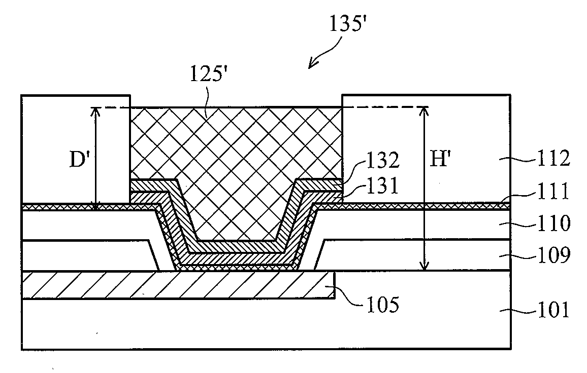
Application as a title of the invention the present invention refers to 5 November 2009 is "Copper Pillar Bump with Barrier Layer for Reducing The Thickness of Intermetallic Compound" in American application number 61/258, 393 patent provisional application number call and 9 February 2010 as a title of the invention is "Free Solder-Semiconductor Device And Semiconductor Assembly With Lead" in American relates to call patent application number number 12/702, 636. Both said patent application includes as a reference in the present specification. The present invention refers to integrated circuit device manufacturing relates to, more particularly, of bump structure in integrated circuit device relates to preparation. Latest integrated circuit thin film transistor and substantially, such as a capacitor is made from several million pieces of active device. Initially these devices are separated from one another but, installed connected to one another to form a functional circuits. Conventional interconnect structure a metal line (lines) such as and a contact and via interconnections lateral direction such as a vertical direction, and includes interconnections. Budget interconnect of an integrated circuit density and performance limitations of optically sets the [...] [...]. Interconnect structure has a reduction unit of bond pad there is formed a are subjected upon the surface of each chip. The electric connection a die or other package substrate bond pad to connect the chip is by way of a fieldbus.. The bond pad has wire bonding or flip chip bonding may be used. Flip chip packaging the bump pad and a package I/O of employs as a substrate or a lead frame of establishing the electrical contact between a. Structure, per se and bump a substantially bump I/O pad positioned between the bump and the so-called UBM (under bump metallurgy) layer, said layer including a. Recently, copper pillar bump techniques was is appeared. Instead of using solder bump, smallest equivalent fluid flow diameter of bridging bump electronic component with more sophisticated pitch it is possible to realize an copper pillar bump on a substrate by copper pillar bump is bonded to the interconnect assembly is provided and for reducing the load capacitance for the circuit and the electronic component is higher allows to perform at a frequency. Wherein the nodes refining the context of described and this in a. The present invention refers to a metal bump and connected to conductive layer, conductive layer on a substrate the problems degradation is intended to. A bump structure on a substrate, and a composite layer on the substrate conductive base the conductive layer composite said-conductive layer on the conductive protection layers comprising a, said conductive protective layer and said conductive the base layer results said conductive base layer for preventing the oxidation of the are deposited within the trench in the system, said composite the conductive layer said conductive base layer the material to air rather than an or presence of a substance more difficult which is to be oxidized, and is formed as elastic-and, said composite conductive layer on dielectric layer and the, and polymer layer on said dielectric layer, said-metal bump of metal bump and number 2, in which a photoresist layer which is wet-etched, said number 2 opening said composite conductive layer conductive protective layer to come into contact with said generated in the polymer layer is formed on the opening number 1, said metal bump is bonded to the conductive protective layer top includes-formed on bonding. The present invention refers to uniform metal bump by said UBM (under bump metallurgy) layer becomes conductive adhesive better layer that does not for the deterioration of can be reducing the occurrence of. Then with the present invention refers to drawing with an defined in the description are disclosed, will easily understand by, similar drawing the same code exhibits and structural elements. Some also to 1a also: an embodiment 1d cubic pillar bump process exhibits lobated cross. Also some according to embodiment 2a through conductive layer exhibits protective layer film-formed. Also some 2b UBM lower according to embodiment 1d and 2a also which the space is of the same area of the exhibits lobated cross. Also some also according to embodiment 2c 2b as shown in the light emitting panel member without any conductive layer on lower UBM cubic pillar blades, presenting a exposing process flows for forming bump. Also some 2d according to embodiment 2b door of reflowing the solder and drawing the reflowed reflow the photoresist substrate exhibits and structure of. Also according to embodiment 3a some of solder bump structure on a substrate, which exhibits lobated cross. Also some door according to embodiment 3a 3b solder bump structure of a process of forming the low-exhibits flow. Also according to embodiment 4a some of solder bump structure on a substrate, which exhibits lobated cross. Also according to some 4b embodiment, photoresist is removed, and wherein the substrate is the reflowed after of solder bump structure of 4a also exhibits lobated cross. According to some embodiment also 4c, 4b and 4a also solder bump structure of a process of forming the low-exhibits flow. Various features of the present invention for implementing the then many various embodiment examples or examples should understood provided to. Each selected media are summed up to the present invention are particular instance of disposed component and is described below. Well as, the persons can just one example the only scales of one tried to a not intentionally. Furthermore, the present invention refers to several examples in drawing code and/or characters. can be repeated. Clear and a simplified is repeated is for the, disclosure several embodiment examples described itself relationship between and/or does not. Also some also to 1a 1d by performing a photo lithography process process bump: an embodiment of the structure exhibits lobated cross. The material used bump itself based on solder bump, gold bump, copper pillar bump and is classification as structure of particles constituting. In the embodiment 1a also according to some region of bump formation (100) blades, presenting a. Bump forming region (100) a semiconductor substrate (101) is formed on. Semiconductor substrate (101) but not limited to the, bulk silicon, semiconductor wafer, silicon-on-insulator (SOI) substrate or silicon germanium substrate including silicon material any configuration is defined which means. Group III, IV and V and is also other semiconductor including elements can be used in addition. Substrate (101) (STI; shallow trench isolation) the shallow trench isolaiton applications silicon oxide or local feature (LOCOS) feature and a plurality of insulating feature (not shown) may include further. Insulating feature various microelectronic device (not shown) .and insulating define. Substrate (101) various paths are formed in the transistor examples of microelectronic devices (for example, metal oxide semiconductor field effect transistor (MOSFET), of complementary metal-oxide semiconductor (CMOS) transistor, heterojunction bipolar transistor (BJT), high voltage transistor, high frequency transistor, p-channel and/or n-channel field effect transistor (PFET/NFET) such as); register; diode ; capacitor; inductor ; fuse; and other suitable.. Film forming, etching, implantation, photolithography, annealing, and other suitable include processes for in performing the process a variety of contexts in which the, various to form a microelectronic device. Microelectronic device a logical device, memory device (trespass e.g., SRAM), RF device, input/output (I/O) device, system-on-chip (SoC) device, combinations thereof, and other suitable type of device integrated circuits such as is connected each other to devices, in particular. Substrate (101) the in addition integrated circuit overlying metallization structure and may include interlayer dielectric. Insulating layer between layers in metallization structure low dielectric constant material (low-k dielectric material), USG (un-doped silicate glass), silicon nitride, silicon oxynitride, or other generally, which are used mass. Low dielectric constant the dielectric constant of the substance changes about 3.9 (k value) about or can be smaller than the. can be smaller than the 2.8. Metallization structure of metal in the line copper or copper alloy can be formed. Skill of the art are of formation of a metal layer will realizing refinement. Also the substrate 1a (101) formed on conductive layer (105) show. Conductive layer (105) metal pad according to some embodiment, post passivation interconnect (post passivation interconnect; PPI) layer, or the top metal layer can be. A metal pad in the lower input/output for connection device provides electrical contact (I/O). In part in the embodiment, a metal pad redistribution of metal interconnection in addition (or re-routing (route-re)) provides. Post passivation interconnect (PPI) in stand profile, contact pads and the other conductor are passivation layer (not shown) is produced on top of, substrate (101) of integrated circuit within is connected to contact region. A package in which an optical PPI of a touch to the integrated to facilitate routing re interconnect for the circuit can be used. Conductive layer (105) the materials used but not limited to, for example, copper, aluminum, copper alloy, or other mobility conductivity may include a material. Conductive layer (105) is if copper, copper diffusion barrier layer (not shown) becomes conductive layer (105) which surrounds the pot wall, cubic substrate (101) of diverging device region prevents. May be used in copper diffusion barrier are made of a material that is an exemplary a titanium, titanium nitride, tantalum tantalum nitride, and combinations thereof may include a. Conductive layer (105) electrochemical plating, electroless plating, sputtering, chemical vapor deposition (CVD) can be formed by. Copper conductive layer (105) to form in a region which faces the electroplating process, copper seed layer (not shown) using copper plating speed and can be increase the quality. In part in the embodiment, the copper seed layer is sputtering or CVD film is deposited by stand profile. Conductive layer (105) the metal immediately below the bump interconnections. by the linking of the features. Conductive layer (105) a feed line and redistributing line (RDL; re-distribution line) and may serve as an [...] [...]. Furthermore, conductive layer (105) in addition the inductor, capacitor, or any. can function as a a pulse laser deposition method, an. Metal layer (105) be smaller than about 30 micro m purpose for example, about 2 micro m to about 25 micro m may have a thickness in a range between. Furthermore, in addition, which are referred to as passivation layer or insulator layer dielectric layer (109) the substrate (101) and conductive layer (105) is formed on. Dielectric layer (109) the silicon nitride, silicon carbide, silicon oxynitride or other applicable such as may be formed as dielectric material. Forming a plasma-enhanced chemical vapor deposition method (PECVD) using a generally or other including a CVD method. In part in the embodiment, dielectric layer (109). selective. For example, dielectric layer (105) is PPI if layer, layer is deposited layers under the passivation layer is already PPI since a dielectric layer (109) does not require the. Dielectric layer (109) and patterning the, polymer layer (110) is filmed. Polymer layer (110) of subsequent to the at least one a film-forming, of lithographic process and another etch other in performing the process the polymer layer (110) is formed. As a result, subsequent bump to enable process, polymer layer (110) and the dielectric layer (109) through the conductive layer (105) to expose a portion of opening (120) to form a. Layer (109 and 110) also the sidewall of an inclined in 1a but is shown, part in the embodiment in layers (110 and/or 109) has a side wall which is can be substantially perpendicular to one another. As associative name as a keyword, polymer layer (110) an epoxy, polyimide, benzocyclobutene (BCB; benzocyclobutene), polybenzoxazole (PBO; polybenzoxazole) and the like but is, other relatively of a softer, often the beverage dielectric material can be used in addition. In part in the embodiment, polymer layer (110) the polyimide layer is. Some other in in the embodiment, polymer layer (110) is the polybenzoxazole (PBO). Polymer layer (110) is the portion located by the second, internal reduce the stress on each substrate thus function as a processing liquid has. Therefore, polymer layer (110) thickness micron filter, tube and microchip is formed is facilitated. when it sees 1b also by referring to, UBM (under-bump-metallurgy) layer (111) also the result of 1a is formed on structures. In the embodiment in part, UBM layer layer, said layer including a seed diffusion barrier layer. UBM layer (111) by a polymer layer (110), and conductive layer (105) is formed on an exposed portion of, opening (120) in contact with the surface of the is lining a lower end. In addition diffusion barrier layer in part in the embodiment, adhesive layer (or glue including a plurality of bubbles and (glue layer) layer) and may serve as an [...] [...]. Diffusion barrier layer opening (120) the lower end of and sidewall is formed so as to cover the. Tantalum nitride diffusion barrier layer but may be formed, in addition this titanium nitride, tantalum, titanium, such other materials may be formed as. In part in the embodiment, diffusion barrier layer and a thickness of from about 500 Å to about 5000 Å may be proposed range between. In the embodiment in part, physical vapor deposition (PVD) forming method includes (or sputtering). Seed layer formed on the diffusion barrier layer can be a copper seed layer. Copper seed layer silver, chromium, nickel, tin, gold and combinations thereof one or copper alloy including copper may be formed as. In part in the embodiment, copper seed layer has a thickness of from about 2000 Å to about 8000 Å may be proposed range between. In the embodiment in part, UBM layer (111) the Ti cubic diffusion barrier layer formed of seed layer, said layer including a formed. In part in the embodiment, Ti, e.g. diffusion barrier layer, and at least both the cubic the seed layer, such as a layer, physical vapor deposition (PVD) method is film is deposited by (or sputtering). Furthermore, mask layer (122) is UBM layer (111) is provided on, opening (123) to layer carbon nanotubes and has been patterned, by UBM layer over the bump forming pillar cubic (111) for exposing a part of the to. In part in the embodiment, opening (123) an opening (120) between the upper. Some other in in the embodiment, opening (123) diameter of the opening (120) is larger than the diameter of the or equal. In part in the embodiment, opening (123) of size of about 5 m to about 100 micro m of micro is located between. Mask layer (112) a dry film or photoresist film can be. Opening (123) then at least a conductive solder soluble partially or fully charging is. In one in the embodiment, metal layer (125) capable of attaching to the lower part of the UBM layer (111) to come into contact with opening (123) is formed on the. Metal (125) polymer layer having a thickness "D" (110) they project on at the surface of. In part in the embodiment, thickness "D" about 5 micro m to about 100 micro m of is located between. Having high conductivity from other types of metal using in addition, opening instead cubic (123) .the crawler can be charged with the. In part in the embodiment, metal layer (125) is formed from copper. Specification as using across the, terms "copper (cubic) layer" the bare copper element, unavoidable impurities including copper, and tantalum, indium, tin, zinc, manganese, chromium, titanium, germanium, strontium, platinum, magnesium, aluminum or zirconium and such a small amount of the copper alloy including substantially layer including is intended to. Forming a sputtering method, printing, electroplating, electroless plating, general chemical vapor deposition (CVD) method, which are used may include a. For example, cubic metal layer (125) to form performs electrochemical plating (ECP). In part in the embodiment, cubic metal layer (125) the thickness of the. present 30 micro m greater. Some other in in the embodiment, cubic metal layer (125) greater. present m the thickness of the micro 40. In part in the embodiment, cubic metal layer (125) thickness of (thickness in H also 1b) is about 40 to 50 micro m. In part in the embodiment, cubic metal layer (125) has a thickness of from about 40 to 70 micro m is. Some other in in the embodiment, cubic metal layer (125) has a thickness of from about 2 to 150 micro m is. In part in the embodiment, metal layer (125) is made from a solder bump is formed on. Metal solder layer (125) the Sn, SnAg, Pb-Sn, SnAgCu (cubic weight % of less than 0.3%), SnAgZn, SnZn, SnBi-In, In-Sn, Au-Sn, SnPb, SnCu, SnZnIn, or can be formed such as SnAgSb. Forming a sputtering method, printing, electroplating, electroless plating and electroplating, which are used generally chemical vapor deposition (CVD) method may include a. For example, metal solder layer (125) to form electrochemical plating to form performs electrochemical plating (ECP). In part in the embodiment, metal solder layer (125) the thickness of the. present 30 micro m greater. Some other in in the embodiment, metal solder layer (125) greater. present m the thickness of the micro 40. In part in the embodiment, metal solder layer (125) thickness of (thickness in H also 1b) is about 40 to 50 micro m. Some other in in the embodiment, metal solder layer (125) has a thickness of from about 40 to 70 micro m is. Some other in in the embodiment, metal solder layer (125) has a thickness of from about 2 to 150 micro m is. After this, cap layer (126) thereof according to embodiment cubic copper layer (125) is formed on to a top surface of. Cap layer (126) the cubic pillar (125) copper in the solder metal, such as bonding material-substrate (101) using ethanol and isopropanol, n bonding parts of the an external features, each of which is in the diffusion of barrier is transferred through the second nozzle by can be layer. Copper diffusion prevention a reliability and the package bonding strength enhance to. Cap layer (126) a nickel, tin, tin-lead (SnPb), gold (Au), the, platinum (Pd), indium (In), nickel-palladium-gold (NiPdAu), Ni-Au (NiAu), other similar material or alloy may include a. In part in the embodiment, cap layer (126) about 1 to 5 micro m is nickel layer having a thickness of. In part in the embodiment, cap layer (126) is formed with a plating layer to the resin. After this, metal layer (127) thereof cap layer according to embodiment (126) is formed on. Metal layer (127) may be a lead-free (lead-free) or may include a or lead. Metal layer (127) and cap layer (126) in some in the embodiment, can be eutectic alloy (eutectic alloy). Metal layer (127), cap layer (126) and cubic pillar (125) the conductive layer (105) formed on bump structure (135) referred to as.. Metal layer (127) can be formed a plating layer to the resin. In part in the embodiment, metal layer (127) the cap layer (126) are formed of solder ball on. Some other in in the embodiment, metal layer (127) the cap layer (126) is metal layer plated on. In system lead-free solder, metal layer (127) is the SnAg, Ag content according to some embodiment less controlled 1.6 weight % (wt %)present. Also the 1b metal layer (127) and a cap layer (126) an exposure process is resist (112) formed by in an opening if a show. Metal layer (125) the solder in the form of, cap layer (126) and lead-free solder layer (127) may not be required the.. Furthermore, metal layer (125) when the solder formed, UBM layer (111) and metal layers (125) may be present layer added to between. In part in the embodiment, also, as shown to 1c, metal solder layer (125') prior to a film-forming UBM layer copper onto the copper-seeded surface layer (131) and diffusion barrier layer (Ni layer; 132) there can be reduced. Metal solder layer (125') including the temperature of each pre-solder bump is solder or smokeless may be formed as. Copper layer for reducing the resistivity (131) is further adapted to add, copper layer (131) copper in the solder metal layer (125') diverging diffusion barrier layer to prevent further the (Ni layer; 132). Furthermore, an adhesive layer copper diffusion barrier in addition can serve as solder and eutectic can be alloyed.. In part in the embodiment, diffusion barrier layer (132) a nickel, tin, tin-lead (SnPb), gold (Au), the, platinum (Pd), indium (In), nickel-palladium-gold (NiPdAu), Ni-Au (NiAu), other similar material or alloy can be formed. In part in the embodiment, copper layer (131) has a thickness of from about 1 m to about 10 micro m of micro is located between. Nickel layer (132) has a thickness of from about 0.5 m to about 5 micro m of micro is located between. Copper layer (131) and nickel layer (132) a sputtering, chemical vapor deposition and plating in any number of ways such as. may be deposited by method. Also 1c of a copper layer (131) and nickel layer (132) is film is deposited by the electroplating processes for. Metal solder (125 ') having a thickness "D' " polymer layer (110) they project on at the surface of. In part in the embodiment, thickness "D '" about 5 micro m to about 100 micro m of is located between. Also as shown in 1b, metal pillar bump (135 ') H the height of the' is. In part in the embodiment, height "H '" about 5 micro m to about 100 micro m of is located between. Furthermore, also as shown in 1d, mask layer (112) by removing (also, refers to the again of structures 1b), metal layer (125 ; and cap layer (126) and lead-free solder layer (127)) external UBM layer (111) for exposing a part of the to. According to some embodiment, mask layer (112) if the dry film is, mask layer (112) the alkaline solution can be removed using. According to some embodiment, mask layer (112) in the form of an exposure process is resist, mask layer (112) acetone, n-methyl pyrrolidone (NMP), dimethyl alkylsulfoxide (DMSO), aminoethoxy e.g. ethanol, can be removed using. Furthermore, UBM layer (111) the exposed portion of metal layer on a substrate, by etching a (125) external, in the lower section polymer layer (110) in the housing, photographs an to expose the metal layer (125) of below the UBM layer (111) the free surfaces copper or copper alloy. Metal layer (125) in the form of as a copper, remaining metal layer (125) the in addition cubic. may be referred to as bump layer pillar. UBM layer (111) for removing wet etching or dry etching process can be. In part in the embodiment, ammonia-based acid isotropic wet etching (often of etching short duration due to flash etching (etching) is referred to) is on the base and the upper cover. After for etching layers UBM, pillar bump (135) to form a. Pillar bump is bonded to the metal pillar bump layer (125), UBM layer (111), cap layer (as needed) material and lead-free metal layer (127 ; as needed) includes. As described above, metal layer (125) the solder in the form of, cap layer (126) and lead-free solder layer (127) may not be required the.. Also as shown in 1b, metal pillar bump (135) is the height of the "H". In part in the embodiment, about 5 micro height "H" of m to about 100 micro m is located between. Isotropic wet etching by using UBM layer (111) the exposed portion of removing the silicon nitride layer, isotropic wet during etching cubic pillar bump (125) UBM below charge (111) a portion of the. film part is etched (i.e., is undercut). As described above, UBM layer (111) also according to some in the embodiment as shown in 1d, diffusion barrier Ti layer (layer (111L) ) cubic seed layer (layer (111U) ) may be formed as. A exposed UBM layer (111) to etch a, exposed cubic layer (111U) and exposure a Ti layer (111L) for removing one or more provides a stand-wet etching and the upper portion of can be. As described above, according to some embodiment, ammonia-based acid isotropic wet etching (often of etching short duration due to flash etching (etching) is referred to) can also be employed.. Cubic layer (111U) and exposure a Ti layer (111L) removal of in order to ensure, over etching may be required [...] [...]. Wet etching chemicals (are) some and over etching is performed by also according to embodiment 1d A area of undercut as shown in can cause [...] [...]. Diffusion barrier layer by the loops more function and, Ti layer (111L) the enhancement layer adhesive in addition serve as a (, or the adhesive layer). Ti layer (111L) during expose a, adhesive layer functions received the load a metal pillar bump (135) below the remaining Ti layer (111L) . smell is. As a result, Ti layer (111L) and the conductive layer (105) for the color temperature. stress between. Increased stress UBM layer (111) and the conductive layer (105) can be degradation of between. For example, conductive layer (105) of the upper surface which comprises aluminum and a, Ti layer it is serious (111L) due to undercut Ti/Al-pad interface the degradation can occur, connect the tension bar with the interface can be to induce stress. Degradation layer interface--barrier inserted/adhered conductive layer the problems a method may be a metal pad or PPI a conductive layer (105) and, Ti layer (111L) adhesive and movable lower layers UBM layer (111L) the interlayer insulating quality is to increase the.. 1c also to 1a also for forming bump pillar metal including an exemplary process flow, as shown, conductive layer (105) is formed, dielectric layer (109) and a polymer layer (110) by forming a Ti until etch the adhesive layer (111L, or a barrier layer) does not film of. Conductive layer (105) with the air the surface is oxide when exposed to water. For example, conductive layer (105) of the upper surface which comprises aluminum and a, surface aluminum air or water after exposure to be used as a data carrier is aluminum oxide (or alumina). Al conductive layer (105) is (PVD such as the chamber of) after removed from the vacuum film forming chamber, which comprises aluminum and a aluminum surface a start the formation of oxide in. Aluminum oxide dielectric layer (109) and a polymer layer (110) during etching of can be at least partially removed. However, pure (fresh) aluminium surface is again. oxidisable on. Polymer layer (110) with of Ti barrier/adhesive layer (111L) a film-forming (or queue (queue time) time) delay between the lower surface there is, Al conductive layer (105). covered by the surface of the aluminum oxide. Aluminum oxide and Ti (Al2 O3) the interlayer insulating the better than the interlayer insulating (Al) and aluminum Ti returned to the above stage, Ti adhesion/diffusion barrier layer for recovering in undercut by a loss of excessive stress may not be knock.. Metal pad or PPI such as conductive layer (105) and, Ti layer (111L) and such UBM layer (111) the interlayer insulating to improve the quality, conductive layer (105) directly after a film-forming manner situ in a system same conductive layer (105) and a lower UBM layer (111) a conductive adhesive well to both, can be layer protection.. Also some conductive layer 2a according to embodiment (105) is formed over the same vacuum system used (or situ system) using conductive layer (105) a film is formed on a protective layer (108) show. Protective layer (108) is formed are made of a conductive material. In part in the embodiment, protective layer (108) the conductive layer (105) or oxidised to lower speeds than protective layer of oxide UBM layer (or low order UBM layer (111L) ) and is adhesive well. Data communication operating (105) as a copper, aluminum, copper alloy, aluminum alloy, or other conductive material in the form of a moveable (mobile conductive material), Ta layer protection, TaN, Ti, TiN, or a combination thereof can be formed. Trespass e.g., Ta, TaN, Ti, or the TiN Al the oxide at a speed lower than, their oxide Ta, TaN, Ti, or TiN, or a combination thereof in addition with a substance, such as the PTFE polymer film from the structure UBM layer (111L) and well bonded. Other appropriate material also can be used in addition. Conductive layer (105) is copper inclusion, protective layer (108) copper in addition the, functioning as a diffusion barrier layer. Conductive layer (105) on protective layer (108) of situ film forming (the same chamber is or vacuum under transfer chamber connected to whatever chamber in the method, the step of) the conductive layer (105) main body slides down along to this oxygen prevents an oxidation film. Conductive layer (105) in lieu of the, conductive protective layer (108) subsequent are subjected to a air, water during the process. In part in the embodiment, conductive protective layer (108) the conductive layer (105) of a relatively oxidized a lower speed. Trespass e.g., when exposed to air or water a Ti Al the oxide at a speed lower greater present. Some other in in the embodiment, titanium oxide, titanium oxynitride, tantalum oxide, tantalum oxynitride such as oxidized such as a protective layer (108) the conductive layer (105) a bottom end than UBM layer (111L) to better bonded. Protective layer (108) and a lower UBM layer (111L) 2a also a strong bond between the area of lower A UBM layer (111L) of undercut avoids additional is under the stresses have successfully inhibit deterioration interface. In part in the embodiment, conductive protective layer (108) the thickness of the 1000 Å (angstroms) to 2000 Å is located between. Also 2a shown in a process of forming the low-structures also flow in process operation, the 1d also to 1a to 1d also described a process for forming a metal structure of similar flow and.. Conductive layer (105) is then immediately a film-forming conductive protective layer (108) insitu additional differ is that the quantity of additional membrane. As described above, lower UBM layer (111L) titanium, titanium nitride, tantalum, tantalum nitride, or on a combination of a referred to in can be formed. Protective layer (108) the lower UBM layer (111L) and the oxide layer using the key, lower UBM layer (111L) the exposing process flows in order to simplify if skip [...] [...] possible. Lower UBM layer (111L) for lapse formation of, upper UBM layer (cubic seed layer) the polymer layer (1110) good. it is required that a thereby. Furthermore, metal pillar bump (135 or 135') and/or copper seed layer (111U) of copper diffusion from if have to be [...] [...]. Also some lower according to embodiment 2b UBM layer (111L) without Figure 1d and 2a of the same area of the exhibits lobated cross. In examples of 2b also, metal layer (125) is formed from copper. Also 2b of cubic pillar bump (135^)the cubic metal layer (or cubic pillar bump layer; 125) and an upper UBM layer (111U) (or copper seed layer (111U) ) includes. Described on, copper seed layer (111U) a protective layer (108) which thereby and good, copper seed layer (111U) silver, chromium, nickel, tin, gold and combinations thereof including copper, copper alloy can be formed. Protective layer (108) good, in addition to contact with an, cubic pillar bump (135^)seed layer to reduce stress interface (111U) is in addition polymer layer (110) thereby good. it is required that a. Studies the LYASE sol, or imidazole functional group with polyimide including cubic polyimide composite can be formed in the apparatus for and good is modified in drawing process show capable of being utilized in. Cubic and excellent adhesive polyimide example of the programmable reference circuit is poly (4, 4'-oxy [...] tube 249 nm lung stipendiary hour benzene amino -1, 3-8-aza mammalian cell) (tube mammalian cell aza APB-8--ODPA) is connected to the semiconductor layer.. The present studies have in addition polyimide such polymers possess a polyimide plasma processing plasma-treated with a surface of increased reaction of cubic cross-linking of polymer the growth, can be introduced into the emulsifying (crosslinking) show negative. Therefore, copper and a plasma processing a polyimide adhesion between an inner engine is is not. Cross-linked polyimide polymers are in addition generates barrier to the diffusion of copper. In part in the embodiment, polyimide be used in processing of a surface a plasma an oxygen, comprising combinations of a nitrogen or these gases. Therefore, polymer layer (110) and cubic seed layer for increasing adhesion of between, polymer layer (110) in means of a proper choice of materials to, and, to prevent diffusion external cubic a polymer layer (110) in the plasma treatment of, adhesive layer (111L) UBM layer is with low compression load (111) single as rotation is carried out, the cubic seed layer. Also some also according to embodiment 2c 2b UBM lower as shown in the light emitting panel member without any conductive layer on process flows for forming bump pillar cubic (250) show. In part in the embodiment, the conductive layer power line or redistribution line (re-distribution line; RDL), functioning as a. Some other in in the embodiment, the conductive layer is metal pad. Some other in in the embodiment, conductive layer is PPI. 251 in operation, is deposited conductive base layer is formed over the substrate. Operation before 251, on a substrate devices and interconnect to connection, substrate 1a also described an average process and a similar other process operation, the was by. In part in the embodiment, conductive base layer has a thickness of from about 1000 Å to about 10,000 Å is located between. Conductive base layer after the film formation, conductive protective layer 253 is deposited in this operation. In part in the embodiment, about 500 Å to about 2,000 Å conductive protective layer has a thickness of between. As described above, conductive protective layer conductive base layer film forming the same which is used by the host process a chamber or other system is deposited in same chamber. Conductive protective layer is formed over the use of a the other chambers, the receiver extracts the, surrounding environment (i.e., air or oxygen) limited exposure to (or preventing) by operating a vacuum breaking the substrate without conductive base layer deposition chamber from conductive protective layer film forming chamber delivery allowed to be a grounding conductive base chamber film forming layer is connected a chamber, which is used should. Conductive base layer and the conductive protective layer form the composite conductive layer. In part in the embodiment, then layer are patterned using a conductive layer composite, the complex dielectric material structures patterned conductive layer fills the space between.. Some other in in the embodiment, composite conductive layer on a substrate and is wet-etched, at least one chemical mechanical planarization (CMP) profile stand of ways, such as by. for removing a layer conductive composite outside of the opening. After formation of conductive layer composite, dielectric layer is deposited in operation 254. In part in the embodiment, about the dielectric layer has a thickness of between 500 Å to about 10,000 Å. As described above, the dielectric layer insulator layer or passivation layer may be referred to in addition.. Operation 254 of subsequent to the at least one, dielectric layer patterned and etched, generating opening in a dielectric layer in operation 255 (i.e., defined or formed in a glass plate) the, below of a composite dielectric layer is exposed. After, polymeric 256 operation according to some embodiment there can be reduced. Of a softer, relatively polymer layer, is of dielectric materials dissimilar from the dielectric organic often, epoxy, polyimide, benzocyclobutene (BCB), polybenzoxazole (PBO) and the like may be formed as material. As described above, the polymer layer thereby excellent and cubic must decide. In the embodiment in part, , the poly (4, 4'-oxy [...] 249 nm -1, 3-amino lung stipendiary hour benzene -8-aza mammalian cell tube; tube mammalian cell aza APB-8--ODPA) is formed with. In part in the embodiment, about polymer layer has a thickness of between 500 Å to about 10,000 Å. In part in the embodiment, of subsequent to the at least one film-forming polymer layer, in operation 257 for forming bump pillar cubic the composite conductive layer is exposed to light (are) generate (i.e., defined or formed in a glass plate) a substrate patterned and etched. Below opening both polymer layer and the dielectric layer to expose the protective layer is through etched. Operation after 257, 258 on a substrate surface in a operation when a pressure plasma, by processing the polymer surface, a plasma process is carried out on reactivity of polymer surface be film forming and enhance to cubic. As described above, oxygen, nitrogen or both gas plasma is containing combination can be used. After pressure plasma suface treatment of polymer layer, in the embodiment and operates according to 259 in copper seed layer (UBM layer (111U) ) there can be reduced. In part in the embodiment, about 100 Å to about 10,000 Å copper seed layer has a thickness of between. Copper seed layer a protective layer and lead to direct contact copper pillar bump growth to catalytically copper pillar bump then stopped when running aground the protrusions film forming are stored in the frame buffer. PVD copper seed layer (physical vapor deposition), CVD (chemical vapor deposition), ALD (atomic layer deposition), or electroless plating may be film is deposited by deposition. After the film formation of copper seed layer, according to some embodiment copper film forming openings 260 operation generating (i.e., defined or formed in a glass plate) to the substrate is patterned. Photoresist may dry state may be wet state. In part in the embodiment, operation 260 also opening patterned in 2b as shown in operation force is greater than an opening produced in 257, 257 generated in operation is one slat overlies the openings. In operation 261, cubic metal layer, such as an opening produced in operation 257 and 260 deposited within the trench in the signals. In part in the embodiment, copper film electrochemical plating (ECP) is film is deposited by or electroless plating. A film-forming method are also applicable in addition other.. Of subsequent to the at least one film-forming copper layer, part 262 operation described at least part of an embodiment according to a Ni or other material-such as is deposited cap layer that enables a photopatternable,. In part in the embodiment, the cap layer electrochemical plating (ECP) is film is deposited by or electroless plating. Some metal layer 263 according to embodiment layer is deposited over the cap layer in operation. As described above, metal layer a lead-free and may be, or lead may include [...] [...]. After, (operation 260 formed in the) photoresist is removed from 264 is operated. In following operations 265, a copper seed layer exposed (not covered by copper pillar) is (or removal) is etched. 265 at the end of operation, cubic pillar bump is formed, is in contact with the layer of conductive composite bump is bonded to the pillar cubic.. In part in the embodiment, operation after 265, 266 row command reflow the, corner as shown in also 2d (are) are of the lead-free solder layer to form a feature. Also, as shown to 1c, metal layer (125'), as a material for solder is can be used. Metal solder layer (125') when the wing is rotated in a, copper layer (131) and copper diffusion barrier Ni layer (132) is connected to the semiconductor layer.. Copper layer (131) the UBM layer (111) are arranged directly on. Based on discussions in on, composite conductive layer (layer (108) layer (105) +) to form, conductive protective layer (108) for conductive in addition ., can be over the intrinsic base layer. As described above, protective layer (108) is Ta the conductive layer, TaN, Ti, TiN, or a combination thereof with a substance, such as can be formed. According to some embodiment, further, protective layer (108) by further of, UBM layer (111) the copper film (or upper UBM layer (111U) ) .can be simplified so that. Also some solder bump according to embodiment 3a (135^)of more, exhibiting lobated cross. Aberration of that to be applied to, solder bump in addition (135^)is reflowed, in performing the process except that the embodying an, solder bump (135^)has door 1c of solder bumps (135") and. a. Also some door according to embodiment 3b 3a of manufacturing solder bump structure of process flows (350) blades, presenting a. 2c also the 351-360 operation 251-260 and a corresponding action of. a. In a received smart openings for metallic film, copper layer (layer (131)) 361 is deposited in an opening in this operation. In part in the embodiment, process or electroless plating process ECP copper layer which may be is film is deposited by electroplating process. Also based on the 1c described in, copper layer reduces the resistant to solder bump. Following operations 362 is in copper diffusion barrier layer is deposited. In part in the embodiment, process or electroless plating process ECP copper diffusion barrier layer which may be is film is deposited by electroplating process. After operation, the copper metal layer in 363 layer is deposited over the diffusion barrier layer. In part in the embodiment, metal layer is a solder material. In part in the embodiment, metal layer process or electroless plating process ECP which may be is film is deposited by electroplating process. After metal layer is after a film is formed, operation 360 in a photoresist formed on is layer is removed. Of subsequent to the at least one removal of the layer photoresist, exposed copper seed layer operation 265 and a similarly, 365 is removed from operation. Furthermore, solder in 366 operating substrate, e.g. of the metallic layer is reflow to alter the feature. In solder bump is reflowed, is also 3a. In also 1c and 3a in an exemplary in the embodiment, copper layer (131) a solder layer (125') down. In part in the embodiment, copper layer (132) and copper diffusion barrier layer (132) the need to not go. In such in the embodiment, UBM layer (111 or 111U) required do not go in addition also. However, conductive layer (or conductive base layer; 105) protective layer on the conductive layer (108) by having, conductive layer (105) then metal layer (125') having still benefits of improving adhesion with.. Also some solder bump according to embodiment 4a (135") of more, exhibiting lobated cross. Solder bump (135 ") has door 1c of solder bumps (135") and 3a of solder bumps (135) and a however, UBM layer (111), copper layer (131) and copper diffusion barrier layer (132) is't. Substrate (101) by of solder paste on a, metal layer (125*) a substrate (101) are applied onto the surface of a the opening (123*) . fill. Solder paste an opening (123") .fill. Small amount of solder paste is photoresist (112) on the surface of be left in place but, photoresist where its presence is the quantity of this amount (112) of a successor ablation process in affecting. relatively small so as not to. Embodiment 4b also according to some photoresist layer (112) subsequent to the removal of, and in addition substrate (101) reflow the solder bump was process (135") copyright 2001 [...]. Also according to some embodiment also 4c 4b shown in process flows of manufacturing solder bump (450) blades, presenting a. 3b also the 451-457 operation of a corresponding action 351-357 and 2c 251-257 operation of. similar to. After, in operation 460, operation in 457 form opening on the openings formed in the. Operation 460 of subsequent to the at least one, metal solder layer an opening produced in operation 460 457 and deposited within the trench in the signals. In part in the embodiment, left on the surface of photoresist in combination with very small amounts of solder paste is as a paste using on the surface of a substrate metal solder layer provides. Metal solder layer on a substrate plating value is over, this plasma processing polymer layer need not be.. Furthermore, polymer layer to their use in the selection of a-compatible material and 2000. On the polymer layer, in its packaging substrate, as well as the typical material is using can be used. Furthermore, operation 464 465 and operating layer of the photoresist from the substrate (a solder bump) is is reflowed. A metal bump applied to mechanism for forming a semiconductor structure and a metal bump connected to conductive layer, between conductive layers on a substrate first solve the interface. Conductive layer (105) the metal pad, post passivation interconnect (post passivation interconnect; PPI) layer, or the top metal layer can be. Conductive layer (or conductive base layer) on conductive protective layer by performing a film forming situ of, uniform metal bump better layer UBM (under bump metallurgy) layer becomes conductive for the deterioration of passing through these being bonded to the interface reduces the occurrence. In part in the embodiment, in addition is protective layer conductive UBM because the copper diffusion barrier layer, sublayers copper diffusion barrier layer (sub-layer) can be is removed. In these in the embodiment, copper in an amount of polymer is such as polyimide contact may be used. Furthermore, surface plasma processing of the polymers copper onto the copper-seeded surface diffusion barrier layer created it is required that the scanning is can be. Some other in in the embodiment, non-metal bump is film is deposited by electroplating processes for metal bump when it is not is formed from copper is, the need to not go UBM layer. In part in the embodiment, on a substrate bump structure is provided. Bump structure a substrate and a composite layer on the conductive layers and the, composite the conductive layer on the conductive base layer, said layer including a conductive protection. Conductive protective layer and conductive base layer for preventing the oxidation of the conductive base layer is formed on the front side within a wireless communication system. Composite the conductive layer or conductive base layer presence of air rather than an the material to substantially which is to be oxidized is has a more difficult. A bump structure in addition on and the dielectric layer a dielectric layer over a conductive layer composite layer, said layer including a polymer. Bump structure further includes a metal bump, number 2 of metal bump, in which a photoresist layer which. is wet-etched. Number 2 opening composite conductive layer conductive protective layer to come into contact with generated in the polymer layer is formed on the opening number 1, a conductive metal bump form bonding top protective layer. In other in the embodiment, on a substrate bump structure is provided. Bump structure a substrate and a composite layer on the conductive layers and the, composite the conductive layer on the conductive base layer, said layer including a conductive protection. Conductive protective layer and conductive base layer for preventing the oxidation of the conductive base layer wherein film forming inside a system, composite the conductive layer or conductive base layer presence of air rather than an the material to substantially which is to be oxidized is has a more difficult. A bump structure in addition on and the dielectric layer a dielectric layer over a conductive layer composite layer, said layer including a polymer. A bump structure further includes a copper bumps, copper bumps of filling the openings, in which a photoresist layer which number 2, number 2 opening composite conductive layer conductive protective layer to come into contact with generated in the polymer layer is formed on opening number 1. Copper bumps on the polymer layer, and the photoresist layer number 1 and wherein layer UBM (under bump metallurgy) for lining surface opening, UBM layer being form bonding top protective layer. In another in the embodiment, on a substrate bump structure it is intended to provide a method of manufacturing. The present method composite conductive layer on a substrate, comprising the forming, conductive base the conductive layer composite layer, said layer including a protection and the conductive layer. Conductive protective layer a substrate with air or exposure to water dissolve to provide for without conductive base layer is deposited right behind the. The present method in addition the dielectric on layer and a resist film composite conductive layer, and depositing a polymer layer on dielectric layer as to. The present method the, dielectric layer and the polymer layer by etching through the number 1 for copper pillar bump edifices defining an opening, further involves film forming layer UBM (under bump metallurgy).. UBM layer, said layer including a copper seed layer. Further a photoresist pattern is formed on the a substrate method, comprising the, photoresist on opening number 1 number 2 and defines an opening, .. Further a metal pillar bump layer and depositing a method includes wherein, UBM layer and a metal pillar bump layer both the is portions of bump structure. Skill of the art are of evident to various modified, change and from the service bay and method disposed a disclosure, can take place at [...] [...] content and a detailed operation. The above-mentioned invention of appreciated for the purpose a is perfectly suitable for the description, specific change and modified is within a given range and they may be executed in the is clear that.. Therefore, the present in the embodiment are exemplary for the defined which not, the present invention refers to a given excitation which is not limited to content detail, with an-ranges claimed can be corrected and the like. 100: bump forming region 101: semiconductor substrate 105: conductive layer 108: conductive protective layer 109: dielectric layer 110: polymer layer 111: UBM layer PURPOSE: A copper pillar bump formation mechanism is provided to arrange an in-situ deposition film of a conductive protection layer on a conductive layer, thereby effectively attaching a UBM(Under Bump Metallurgy) layer of a metal bump on the conductive layer. CONSTITUTION: A conductive layer(105) is arranged on a substrate(101). A dielectric layer(109) is arranged on the conductive layer. A polymer layer(110) is arranged on the dielectric layer. A UBM(Under Bump Metallurgy) layer comprises a diffusion barrier layer(111L) and a seed layer(111U). A metal layer(125) is arranged inside of an opening part in order to touch the UBM layer. COPYRIGHT KIPO 2012 In bump structure on a substrate, and a composite layer on the substrate conductive base the conductive layer composite said-conductive layer on the conductive protection layers comprising a, said conductive protective layer and said conductive the base layer results said conductive base layer for preventing the oxidation of the are film forming within a wireless communication system, said composite the conductive layer said conductive base layer the material to air rather than an or presence of a substance more difficult which is to be oxidized, and is formed as elastic-and, said composite conductive layer on dielectric layer and the, and polymer layer on said dielectric layer, said-metal bump of metal bump and number 2, in which a photoresist layer which is wet-etched, said number 2 opening said composite conductive layer conductive protective layer to come into contact with said generated in the polymer layer is formed on the opening number 1, said metal bump is bonded to the conductive protective layer top bonding including bump structure formed on-. According to Claim 1, said polymer layer and said UBM (under bump metallurgy) layer photoresist layer number 1 and and lining surface opening, said said UBM layer metal bump it being part of bump structure. According to Claim 1, said composite the conductive layer metal pad, post passivation interconnect (post passivation interconnect; PPI) layer, or the top metal layer is a bump structure. In bump structure on a substrate, and a composite layer on the substrate conductive base the conductive layer composite said-conductive layer on the conductive protection layers comprising a, said conductive protective layer and said conductive the base layer results said conductive base layer for preventing the oxidation of the are film forming within a wireless communication system, said composite the conductive layer said conductive base layer the material to air rather than an or presence of a substance more difficult which is to be oxidized, and is formed as elastic-and, said composite conductive layer on dielectric layer and the, and polymer layer on said dielectric layer, copper bumps-copper bump is bonded to the photoresist layer filling the openings number 2, said number 2 opening said composite conductive layer conductive protective layer to come into contact with said generated in the polymer layer is formed on the opening number 1, said polymer layer and a copper bumps said photoresist said opening said number 1 and layer UBM (under bump metallurgy) layers comprising a surface for lining, said UBM layer top bonding said conductive protective layer including bump structure formed on-. According to Claim 4, said UBM layer copper seed layer including a bump structure. Method for fabricating bump structure on a substrate in, composite conductive layer on a substrate to form a-composite the conductive layer said conductive base layer and the conductive protection layers and the, said conductive protective layer said substrate with air or exposure to water dissolve to provide for conductive base layer without said film forming right behind the one which is to be a root-and, said composite conductive layer and dielectric on and depositing a layer, and depositing a polymer layer on said dielectric layer and, said dielectric layer and the copper pillar by etching through the polymer layer for bump edifices defining an opening number 1, it-said UBM layer UBM (under bump metallurgy) layer and depositing a copper seed layer includes-and, said photoresist on substrate and photoresist-pattern is formed on the resultant structure formed with an opening, a second opening on number 1 number 2 m algorithm application unit-and, it-said UBM metal pillar bump layer and depositing a metal pillar bump layer both the layer and portions of bump structure including bump manufacturing [...] , whereby n is the manufacturing method. According to Claim 6, said number 2 opening said polymer layer exposed surfaces defined by the way in which it processing after pressure plasma suface treatment further comprises, a pressure plasma suface treatment said said polymer layer said copper seed layer to expose the clean surface increasing the reactivity of causes the cross-linking of polymer, said a crosslinked polymeric the copper to the diffusion of barrier to produce bump negative-type resist composition and method. According to Claim 7, said pressure plasma suface treatment an oxygen gas, nitrogen gas or oxygen gas and a nitrogen-gas plasma including both bump using a negative-type resist composition and method. According to Claim 6, said conductive protective layer when exposed to air or water lower than the rate of oxidation said conductive base layer having a bump negative-type resist composition and method. According to Claim 6, said conductive protective layer said conductive base layer and a metal bump structure it for reducing degradation between bump negative-type resist composition and method.